WO2013190849A1 - 光源装置 - Google Patents
光源装置 Download PDFInfo
- Publication number
- WO2013190849A1 WO2013190849A1 PCT/JP2013/003880 JP2013003880W WO2013190849A1 WO 2013190849 A1 WO2013190849 A1 WO 2013190849A1 JP 2013003880 W JP2013003880 W JP 2013003880W WO 2013190849 A1 WO2013190849 A1 WO 2013190849A1
- Authority
- WO
- WIPO (PCT)
- Prior art keywords
- light source
- source device
- heat transfer
- pattern
- conductive member
- Prior art date
- Legal status (The legal status is an assumption and is not a legal conclusion. Google has not performed a legal analysis and makes no representation as to the accuracy of the status listed.)
- Ceased
Links
Images



















Classifications
-
- H—ELECTRICITY
- H10—SEMICONDUCTOR DEVICES; ELECTRIC SOLID-STATE DEVICES NOT OTHERWISE PROVIDED FOR
- H10W—GENERIC PACKAGES, INTERCONNECTIONS, CONNECTORS OR OTHER CONSTRUCTIONAL DETAILS OF DEVICES COVERED BY CLASS H10
- H10W90/00—Package configurations
-
- H—ELECTRICITY
- H05—ELECTRIC TECHNIQUES NOT OTHERWISE PROVIDED FOR
- H05K—PRINTED CIRCUITS; CASINGS OR CONSTRUCTIONAL DETAILS OF ELECTRIC APPARATUS; MANUFACTURE OF ASSEMBLAGES OF ELECTRICAL COMPONENTS
- H05K1/00—Printed circuits
- H05K1/02—Details
- H05K1/0201—Thermal arrangements, e.g. for cooling, heating or preventing overheating
- H05K1/0203—Cooling of mounted components
-
- H—ELECTRICITY
- H05—ELECTRIC TECHNIQUES NOT OTHERWISE PROVIDED FOR
- H05K—PRINTED CIRCUITS; CASINGS OR CONSTRUCTIONAL DETAILS OF ELECTRIC APPARATUS; MANUFACTURE OF ASSEMBLAGES OF ELECTRICAL COMPONENTS
- H05K3/00—Apparatus or processes for manufacturing printed circuits
- H05K3/10—Apparatus or processes for manufacturing printed circuits in which conductive material is applied to the insulating support in such a manner as to form the desired conductive pattern
- H05K3/20—Apparatus or processes for manufacturing printed circuits in which conductive material is applied to the insulating support in such a manner as to form the desired conductive pattern by affixing prefabricated conductor pattern
- H05K3/202—Apparatus or processes for manufacturing printed circuits in which conductive material is applied to the insulating support in such a manner as to form the desired conductive pattern by affixing prefabricated conductor pattern using self-supporting metal foil pattern
-
- H—ELECTRICITY
- H10—SEMICONDUCTOR DEVICES; ELECTRIC SOLID-STATE DEVICES NOT OTHERWISE PROVIDED FOR
- H10H—INORGANIC LIGHT-EMITTING SEMICONDUCTOR DEVICES HAVING POTENTIAL BARRIERS
- H10H20/00—Individual inorganic light-emitting semiconductor devices having potential barriers, e.g. light-emitting diodes [LED]
- H10H20/80—Constructional details
- H10H20/85—Packages
- H10H20/857—Interconnections, e.g. lead-frames, bond wires or solder balls
-
- F—MECHANICAL ENGINEERING; LIGHTING; HEATING; WEAPONS; BLASTING
- F21—LIGHTING
- F21K—NON-ELECTRIC LIGHT SOURCES USING LUMINESCENCE; LIGHT SOURCES USING ELECTROCHEMILUMINESCENCE; LIGHT SOURCES USING CHARGES OF COMBUSTIBLE MATERIAL; LIGHT SOURCES USING SEMICONDUCTOR DEVICES AS LIGHT-GENERATING ELEMENTS; LIGHT SOURCES NOT OTHERWISE PROVIDED FOR
- F21K9/00—Light sources using semiconductor devices as light-generating elements, e.g. using light-emitting diodes [LED] or lasers
- F21K9/20—Light sources comprising attachment means
- F21K9/27—Retrofit light sources for lighting devices with two fittings for each light source, e.g. for substitution of fluorescent tubes
-
- F—MECHANICAL ENGINEERING; LIGHTING; HEATING; WEAPONS; BLASTING
- F21—LIGHTING
- F21Y—INDEXING SCHEME ASSOCIATED WITH SUBCLASSES F21K, F21L, F21S and F21V, RELATING TO THE FORM OR THE KIND OF THE LIGHT SOURCES OR OF THE COLOUR OF THE LIGHT EMITTED
- F21Y2115/00—Light-generating elements of semiconductor light sources
- F21Y2115/10—Light-emitting diodes [LED]
-
- H—ELECTRICITY
- H05—ELECTRIC TECHNIQUES NOT OTHERWISE PROVIDED FOR
- H05K—PRINTED CIRCUITS; CASINGS OR CONSTRUCTIONAL DETAILS OF ELECTRIC APPARATUS; MANUFACTURE OF ASSEMBLAGES OF ELECTRICAL COMPONENTS
- H05K2201/00—Indexing scheme relating to printed circuits covered by H05K1/00
- H05K2201/10—Details of components or other objects attached to or integrated in a printed circuit board
- H05K2201/10007—Types of components
- H05K2201/10106—Light emitting diode [LED]
-
- H—ELECTRICITY
- H05—ELECTRIC TECHNIQUES NOT OTHERWISE PROVIDED FOR
- H05K—PRINTED CIRCUITS; CASINGS OR CONSTRUCTIONAL DETAILS OF ELECTRIC APPARATUS; MANUFACTURE OF ASSEMBLAGES OF ELECTRICAL COMPONENTS
- H05K2201/00—Indexing scheme relating to printed circuits covered by H05K1/00
- H05K2201/10—Details of components or other objects attached to or integrated in a printed circuit board
- H05K2201/10227—Other objects, e.g. metallic pieces
- H05K2201/10272—Busbars, i.e. thick metal bars mounted on the printed circuit board [PCB] as high-current conductors
-
- H—ELECTRICITY
- H10—SEMICONDUCTOR DEVICES; ELECTRIC SOLID-STATE DEVICES NOT OTHERWISE PROVIDED FOR
- H10H—INORGANIC LIGHT-EMITTING SEMICONDUCTOR DEVICES HAVING POTENTIAL BARRIERS
- H10H20/00—Individual inorganic light-emitting semiconductor devices having potential barriers, e.g. light-emitting diodes [LED]
- H10H20/80—Constructional details
- H10H20/85—Packages
- H10H20/852—Encapsulations
- H10H20/853—Encapsulations characterised by their shape
-
- H—ELECTRICITY
- H10—SEMICONDUCTOR DEVICES; ELECTRIC SOLID-STATE DEVICES NOT OTHERWISE PROVIDED FOR
- H10W—GENERIC PACKAGES, INTERCONNECTIONS, CONNECTORS OR OTHER CONSTRUCTIONAL DETAILS OF DEVICES COVERED BY CLASS H10
- H10W72/00—Interconnections or connectors in packages
- H10W72/851—Dispositions of multiple connectors or interconnections
- H10W72/874—On different surfaces
- H10W72/884—Die-attach connectors and bond wires
-
- H—ELECTRICITY
- H10—SEMICONDUCTOR DEVICES; ELECTRIC SOLID-STATE DEVICES NOT OTHERWISE PROVIDED FOR
- H10W—GENERIC PACKAGES, INTERCONNECTIONS, CONNECTORS OR OTHER CONSTRUCTIONAL DETAILS OF DEVICES COVERED BY CLASS H10
- H10W90/00—Package configurations
- H10W90/701—Package configurations characterised by the relative positions of pads or connectors relative to package parts
- H10W90/751—Package configurations characterised by the relative positions of pads or connectors relative to package parts of bond wires
- H10W90/754—Package configurations characterised by the relative positions of pads or connectors relative to package parts of bond wires between a chip and a stacked insulating package substrate, interposer or RDL
Definitions
- the present invention relates to a light source device.
- a light emitting device which constitutes a line light source by arranging a plurality of light emitting modules in a line, as shown in, for example, Japanese Unexamined Patent Publication No. 2010-98302.
- a light emitting device 125 in which light emitting modules 101 having the same structure are point-symmetrically arranged and connected to each other.
- Each light emitting module 101 includes a substrate 102, a plurality of light emitting diodes 111, a connection connector 115, and an end connector 121.
- the substrate 102 is rectangular as shown in FIGS. 38 and 39.
- the substrate 102 is formed mainly of an insulating material (for example, glass epoxy resin).
- the substrate 102 has a circuit in which the light emitting diodes 111 are connected in series on the surface to be the light emitting surface. In addition, this circuit is covered with an insulating film consisting of a white-based film.
- the circuit is formed of a first conductor pattern 103, a second conductor pattern 104, a plurality of third conductor patterns 105, and a fourth conductor pattern 106.
- Each conductor pattern 103, 104, 105, 106 is comprised with metals, such as copper foil.
- the first conductor pattern 103 and the second conductor pattern 104 are respectively provided at both ends of the substrate 102 in the longitudinal direction.
- the plurality of third conductor patterns 105 are provided along the longitudinal direction of the substrate 102 between the first conductor pattern 103 and the second conductor pattern 104.
- the fourth conductor pattern 106 is provided along the long side of the substrate 102 so as to extend from the side where the first conductor pattern 103 is provided to the side where the second conductor pattern 104 is provided.
- One end portion 106 a of the fourth conductor pattern 106 is aligned with the first conductor pattern 103 along the short side of the substrate 102.
- the other end 106 b of the fourth conductor pattern 106 is aligned with the second conductor pattern 104 along the short side of the substrate 102.
- the first conductor pattern 103 to the third conductor pattern 105 secure as large an area as possible on the substrate 102 in order to function as a heat spreader.
- a metal foil 107 is provided which spreads over substantially the entire area.
- the metal foil 107 is made of copper foil or the like and is covered with an insulating film.
- connection connector 115 is positioned at the center in the width direction at one end in the longitudinal direction of the substrate 102 and mounted on the surface of the substrate 102.
- the end connector 121 is positioned at the center in the width direction at the other end in the longitudinal direction of the substrate 102, and is mounted on the surface of the substrate 102.
- the end connector 121 is connected to the shorting strip 131 or the power supply line 135.
- the shorting pieces 131 and the power supply lines 135 are both insulation coated wires.
- the connection connectors 115 of the pair of light emitting modules 101 are connected to each other, and the shorting piece 131 is inserted and connected to the end connector 121 of one light emitting module 101.
- a power supply line 135 is inserted and connected to 121.
- the light emitting module 101 and the light emitting device 125 described above since the heat generated by the light emitting diode 111 is dissipated through the substrate 102, for example, the light output of the individual light emitting diode 111 is increased. When the light output is increased, there is a concern that the temperature rise of the light emitting diode 111 can not be sufficiently suppressed. For this reason, in the light emitting module 101 and the light emitting device 125 described above, there is a possibility that the increase in light output may be limited.
- the connection connector 115 is mounted on the surface of the substrate 102 at one end in the longitudinal direction of the substrate 102, when viewed as a line light source, There is a concern that the distance may change and one end of the substrate 102 may become dark. Further, the light emitting device 125 can make the distance between the light emitting diodes 111 constant if the arrangement pitch of the light emitting diodes 111 in the light emitting module 101 is made longer, but the individual light emitting diodes 111 light up as particles. There is a concern that it may seem to
- part of the light emitted from the light emitting diode 111 adjacent to the connection connector 115 is blocked by the connection connector 115 to form a shadow, or part of the light emitted from the light emitting diode 111 is the connector There is a concern that the light output may be reduced by absorption at 115.
- the present invention has been made in view of the above-described problems, and an object thereof is to provide a light source device capable of improving heat dissipation and capable of increasing the light output.
- a first aspect of the light source device is a light source device in which a plurality of LED modules are arranged in a specified direction, and each of the LED modules is a long mounting substrate, and a length of the mounting substrate And a plurality of LED chips arranged along the direction.
- the mounting substrate is formed of a long heat transfer portion having a first surface and a second surface on which the LED chip is mounted, and a conductive plate disposed on the second surface, and the LED chip is electrically And a wiring pattern connected to the The said wiring pattern has a terminal piece for electrically connecting said LED modules, and the said heat-transfer part has a notch part which exposes the said terminal piece.
- the terminal piece and the cutout portion are disposed at one end side in the width direction at both end portions in the longitudinal direction of the mounting substrate.
- the LED modules adjacent to each other are arranged such that the terminal pieces are opposed to each other, and a conductive member is arranged so as to cover the terminal pieces opposed to each other and hold the terminal pieces opposed to each other. By being plastically deformed, they are electrically connected to each other.
- the conductive member is cylindrical.
- the conductive member is a member formed by bending a sheet metal into a U-shape.
- each of the terminal pieces is partially inserted with the plastically deformed conductive member. With holes or cutouts.
- the conductive member is a depressed portion recessed from another portion in the conductive member. Equipped with
- the terminal pieces connected by the conductive member extend in the thickness direction of the wiring pattern. It is bent to the said notch part side along.
- the second conductive member is the terminal piece located at the end of the specified direction.
- the heat transfer portion is a surface opposite to the one surface on which the LED chip is mounted.
- a heat transfer plate having the other surface, and an insulating layer disposed on the other surface and having electrical insulation and thermal conductivity.
- the heat transfer plate is formed of a first metal plate
- the conductive plate is formed of a second metal plate. The first metal plate and the second metal plate have different coefficients of linear expansion.
- the insulating layer contains a thermosetting resin and a filler having a thermal conductivity higher than that of the thermosetting resin.
- the heat transfer plate includes an aluminum plate as the first metal plate, an aluminum film, and a reflection enhancing film.
- the aluminum film is disposed on the side opposite to the insulating layer side of the aluminum plate.
- the increase reflection film is disposed on the aluminum film.
- the aluminum film is higher in purity than the aluminum plate.
- the reflection enhancing film is composed of at least two types of dielectric films having different refractive indexes.
- the heat transfer portion is formed of a resin containing a filler and having electrical insulation. Ru.
- the light source device in any one of the first to eleventh aspects, is excited by light emitted from the LED chip and has a wavelength longer than that of the LED chip.
- a wavelength converter including a phosphor that emits light and a transparent material. The wavelength conversion unit is in contact with the heat transfer unit.
- each of the LED chips has a first electrode and a second electrode on one surface in the thickness direction.
- the wiring pattern includes a first pattern and a second pattern.
- the first electrode is electrically connected to the first pattern through a wire
- the second electrode is electrically connected to the second pattern through a wire.
- the heat transfer portion includes through holes through which each of the wires passes.
- a lighting apparatus including a main body and a light source device according to any one of the first to thirteenth aspects.
- the light source device is held by the tool body.
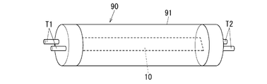
- a lamp comprising: a straight tubular tube main body; and a light source device according to any one of the first to thirteenth aspects, wherein the light source device is provided in the tube main body. It is stored.
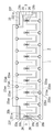
- FIG. 2 is a schematic plan view of the light source device of the first embodiment.
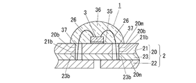
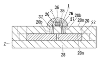
- FIG. 2 is a schematic cross-sectional view taken along line AA of FIG. 1 showing the light source device of Embodiment 1.
- FIG. 2 is a schematic cross-sectional view taken along line BB in FIG. 1, showing the light source device of Embodiment 1.
- FIG. 2 is a partially broken schematic perspective view of the LED module used in the light source device of the first embodiment.
- FIG. 2 is a schematic plan view of an essential part of the LED module used in the light source device according to the first embodiment.
- FIG. 5 is an exploded perspective view of a mounting substrate in an LED module used for the light source device of Embodiment 1.
- FIG. 5 is an explanatory view of a method of manufacturing an LED module used in the light source device of Embodiment 1.
- FIG. 5 is an explanatory view of a method of manufacturing an LED module used in the light source device of Embodiment 1.
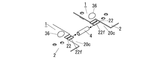
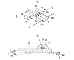
- FIG. 5 is an explanatory view of a method of connecting LED modules in the light source device of Embodiment 1.
- (A) is explanatory drawing of the connection method of LED modules by the other structural example of the electroconductive member in the light source device of Embodiment 1
- (b) is a schematic sectional drawing of the light source device using the electroconductive member of (a) It is.
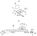
- (A) is explanatory drawing of the connection method of LED modules by the other structural example of the electroconductive member in the light source device of Embodiment 1
- (b) is a schematic cross section of the light source device using the electroconductive member of (a)
- FIG. (A) is explanatory drawing of the connection method of LED modules by the other structural example of the electroconductive member in the light source device of Embodiment 1
- (b) is a schematic sectional drawing of the light source device using the electroconductive member of (a) It is.
- FIG. 5 is an explanatory view of a method of connecting LED modules in the light source device of Embodiment 1.
- FIG. 5 is an explanatory view of a method of connecting LED modules in the light source device of Embodiment 1.
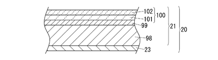
- FIG. 2 is a cross-sectional view of a heat transfer unit provided in the light source device of Embodiment 1.
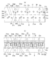
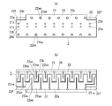
- 5 is a schematic plan view of a light source device of Embodiment 2.
- FIG. FIG. 6 is a schematic cross-sectional view of main parts of a light source device according to a second embodiment.
- FIG. 7 is a schematic plan view of the main parts of an LED module used in the light source device of the second embodiment.
- FIG. 13 is an explanatory drawing of the method of manufacturing the LED module in the light source device of Embodiment 2.
- FIG. 13 is an explanatory drawing of the method of manufacturing the LED module in the light source device of Embodiment 2.
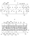
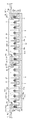
- FIG. 10 is a schematic plan view of the light source device of the third embodiment.
- FIG. 10 is a schematic cross-sectional view of an LED module used in the light source device of Embodiment 3.
- FIG. 10 is a schematic plan view of an LED module used for the light source device of Embodiment 3.
- FIG. 10 is a schematic plan view of an LED module used for the light source device of Embodiment 3.
- FIG. 13 is a plan view of a mounting substrate in an LED module used for the light source device of Embodiment 3.
- FIG. 18 is an explanatory drawing of a method of manufacturing an LED module used for the light source device of Embodiment 3.
- FIG. 18 is an explanatory drawing of a method of manufacturing an LED module used for the light source device of Embodiment 3.
- FIG. 18 is an explanatory drawing of a method of manufacturing an LED module used for the light source device of Embodiment 3.
- FIG. 18 is an explanatory drawing of a method of manufacturing an LED module used for the light source device of Embodiment 3.
- FIG. 18 is an explanatory drawing of a method of manufacturing an LED module used for the light source device of Embodiment 3.
- FIG. 18 is an explanatory drawing of a method of manufacturing an LED module used for the light source device of Embodiment 3.
- FIG. 18 is an explanatory drawing of a method of manufacturing an LED module used for the light source device of Embodiment 3.
- FIG. 18 is an explanatory drawing of a method of manufacturing an LED module used for the light source device of Embodiment 3.
- FIG. 18 is an explanatory drawing of a method of manufacturing an LED module used for the light source device of Embodiment 3.
- FIG. 18 is an explanatory drawing of a method of manufacturing an LED module used for the light source device of Embodiment 3.
- It is a perspective view showing a lighting fixture of an embodiment. It is a perspective view showing a lamp of an embodiment.
- It is a perspective view which shows the light-emitting device of a prior art example.
- It is a front view which shows the light emitting module of a prior art example with a power wire and a short piece.
- It is a rear view of the light emitting module of a prior art example.
- a plurality of LED modules 1 are arranged in a specified direction (left and right direction in FIG. 1), and adjacent LED modules 1 are electrically connected to each other.
- the LED module 1 includes an elongated mounting substrate 2 and a plurality of LED chips 3 arranged along the longitudinal direction (left and right direction in FIG. 1) of the mounting substrate 2.
- the LED modules 1 are arranged so that the specified direction matches the longitudinal direction of the mounting substrate 2.
- the mounting substrate 2 is disposed on the long heat transfer portion 20 on which each LED chip 3 is mounted on the one surface (first surface 20 m) side, and on the other surface (second surface 20 n) side of the heat transfer portion 20.
- a wiring pattern 22 to which the LED chip 3 is electrically connected is formed of the heat transfer unit 20 includes the first surface 20 m on which the LED chip 3 is mounted, and the second surface 20 n opposite to the first surface 20 m.
- the first surface 20m and the second surface 20n are orthogonal to the thickness direction (the direction perpendicular to the sheet of FIG. 1).
- the wiring pattern 22 is formed of a conductive plate.
- the wiring pattern 22 has a first pattern 22a and a second pattern 22b described later.
- the longitudinal direction of the mounting substrate 2 coincides with the longitudinal direction of the long heat transfer portion 20 and the longitudinal direction of the long wiring pattern 22.
- the width direction (vertical direction in FIG. 1) of the mounting substrate 2 coincides with the width direction (short direction) of the heat transfer portion 20 (heat transfer plate 21) and the wiring pattern 22.
- the wiring pattern 22 has terminal pieces 22f that allow the LED modules 1 to be electrically connected to each other at one end in the width direction (direction orthogonal to the longitudinal direction of the mounting substrate 2) at both ends in the longitudinal direction of the mounting substrate 2 doing. Further, the heat transfer portion 20 is formed with notches 20 c at one end side in the width direction at both end portions in the longitudinal direction of the mounting substrate 2 so as to expose the terminal pieces 22 f. Also, the LED modules 1 are electrically connected so as to be plastically deformed so that the conductive members 4 disposed so as to cover both of the opposing terminal pieces 22f hold the terminal pieces 22f. .
- the LED chip 3 has a first electrode (not shown) on one side in the thickness direction (vertical direction in FIG. 1) (the side far from the heat transfer portion 20 in the LED chip 3; near side in FIG. 1; upper side in FIG. 2) And a second electrode (not shown).
- each of the first electrode and the second electrode is electrically connected to the wiring pattern 22 (first pattern 22 a, second pattern 22 b) through the wire 26. That is, the first electrode of the LED chip 3 is electrically connected to the first pattern 22a via the wire 26 (first wire), and the second electrode of the LED chip 3 is via the wire 26 (second wire) Thus, the second pattern 22b is electrically connected.
- the heat transfer portion 20 is formed with through holes 20 b through which the respective wires 26 pass. That is, the heat transfer unit 20 includes the through holes 20 b through which the wires 26 pass. In the first embodiment, the heat transfer unit 20 includes a through hole 20 b through which the first wire 26 passes, and a through hole 20 b through which the second wire 26 passes.
- the heat transfer portion 20 is formed of a first metal plate, and has a long heat transfer plate 21 on which each LED chip 3 can be mounted, and the other surface side of the heat transfer plate 21 has electrical insulation and heat. And an insulating layer 23 having conductivity. The insulating layer 23 is interposed between the heat transfer plate 21 and the wiring pattern 22.
- the insulating layer 23 is disposed between the heat transfer plate 21 and the wiring pattern 22 so that the heat transfer plate 21 and the wiring pattern 22 are not electrically connected.
- the surface of the heat transfer plate 21 opposite to the insulating layer 23 is the first surface 20 m of the heat transfer portion 20. Further, the surface of the insulating layer 23 opposite to the heat transfer plate 21 is the second surface 20 n of the heat transfer portion 20.
- the insulating layer 23 is formed in a long shape.
- the wiring pattern 22 is formed of a conductive plate as described above.
- the conductive plate is a second metal plate having a coefficient of linear expansion different from that of the heat transfer plate 21.
- the mounting substrate 2 is formed in a long shape as a whole, and is configured such that a plurality of (36 in the example of FIG. 7) LED chips 3 can be arrayed and mounted in the longitudinal direction of the mounting substrate 2 .
- the mounting substrate 2 is provided with a predetermined number of sets of two through holes 20b (36 sets in the example of FIG. 7). That is, in the first embodiment, the predetermined number is the same as the number of LED chips 3.
- the through hole 20 b for passing the first wire 26 connected to the first electrode of the LED chip 3 and the through hole 20 b for passing the second wire 26 connected to the second electrode of the same LED chip 3 As a set of through holes 20b.
- the through hole 20 b for passing the first wire 26 connected to the first electrode of the LED chip 3 and the through hole 20 b for passing the second wire 26 connected to the second electrode of the same LED chip 3 are close. Is located in In the first embodiment, the pair of through holes 20 b are aligned in the longitudinal direction of the heat transfer portion 20.
- the number of LED chips 3 that can be mounted on the mounting substrate 2 is not particularly limited.
- metal with high heat conductivity such as aluminum and copper
- the material of the first metal plate is not limited thereto, and may be, for example, stainless steel or steel.
- the heat-transfer plate 21 has a function as a reflecting plate, and it is more preferable to employ
- the first metal plate is an aluminum plate 98, and as shown in FIG. 16, an aluminum film 99 having a purity higher than that of the aluminum plate 98 on the opposite side of the aluminum plate 98 to the insulating layer 23 side.
- the aluminum film 99 is laminated with the reflection enhancing film 100 made of at least two types of dielectric films 101 and 102 having different refractive indexes. That is, the heat transfer plate 21 includes the aluminum plate 98, the aluminum film 99, and the reflection increasing film 100 as the first metal plate.
- the reflection increasing film 100 is disposed on the opposite side of the aluminum plate 98 in the aluminum film 99.
- the aluminum film 99 is formed of aluminum of higher purity than the aluminum plate 98.
- the LED module 1 can make the reflectance for visible light 95% or more.
- a heat transfer plate 21 for example, MIRO 2 and MIRO (registered trademark) of Alanod Co., Ltd. can be used.
- MIRO 2 and MIRO registered trademark of Alanod Co., Ltd.
- the thickness of the heat transfer plate 21 may be appropriately set, for example, in the range of about 0.2 to 3 mm.
- the reflection-increasing film 100 is a two-layer structure in which by laminating a SiO 2 film and a TiO 2 film, may be employed as four-layer structure of alternately laminated SiO 2 film and a TiO 2 film, stacked
- the number is not particularly limited.
- the wavelength region etc. of the light to be reflected can be adjusted by appropriately setting the refractive index and the film thickness of each layer.
- the heat transfer plate 21 is formed with a first through hole 21 b through which each of the wires 26 electrically connecting the LED chip 3 and the wiring pattern 22 can be passed. That is, the heat transfer plate 21 includes the first through holes 21 b that constitute a part of the through holes 20 b. The first through holes 21 b are formed on both sides of the mounting area of the LED chip 3 in the longitudinal direction of the heat transfer plate 21.
- the first through hole 21 b has a circular opening shape.
- the inner diameter of the first through hole 21 b is set to 0.5 mm, but this value is an example and is not particularly limited.
- the shape of the first through hole 21 b is not limited to a circular shape, and may be, for example, a rectangular shape, an elliptical shape, or the like.
- the insulating layer 23 is formed with second through holes 23 b communicating with the respective first through holes 21 b of the heat transfer plate 21. That is, the insulating layer 23 includes the second through hole 23 b that constitutes a part of the through hole 20 b. Therefore, when mounting the LED chip 3 on the mounting substrate 2, for example, the LED chip 3 and the wiring pattern 22 may be formed through the first through holes 21 b of the heat transfer plate 21 and the second through holes 23 b of the insulating layer 23. It can be connected electrically.
- the first through holes 21 b of the heat transfer plate 21 and the second through holes 23 b of the insulating layer 23 constitute the through holes 20 b of the heat transfer portion 20.
- the metal hoop material which consists of strip
- the second metal plate As a material of the second metal plate, copper having a relatively high thermal conductivity among metals (the thermal conductivity of copper is about 398 W / m ⁇ K) is preferable, but not limited to copper, for example, phosphor bronze etc. Or a copper alloy (eg, 42 alloy etc.).
- the thickness of the second metal plate is preferably set, for example, in the range of about 100 ⁇ m to 1500 ⁇ m.
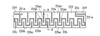
- the wiring pattern 22 has a first pattern 22 a to which the first electrode of the LED chip 3 is connected, and a second pattern 22 b to which the second electrode of the LED chip 3 is connected.
- the first pattern 22a and the second pattern 22b are arranged so as not to be in physical contact with each other.
- the first pattern 22a and the second pattern 22b are each formed in a comb shape in plan view.
- the first pattern 22 a and the second pattern 22 b are arranged so as to intermingle with each other in the direction along the lateral direction of the heat transfer plate 21 (the width direction of the mounting substrate 2). That is, the wiring patterns 22 are arranged in a so-called comb shape.
- the first comb bone portion 22aa of the first pattern 22a and the second comb bone portion 22ba of the second pattern 22b are opposed to each other.
- the first comb teeth 22 ab of the first pattern 22 a and the second comb teeth 22 bb of the second pattern 22 b are in the direction along the longitudinal direction of the heat transfer plate 21 (longitudinal direction of the mounting substrate 2). They line up alternately through gaps. That is, the first pattern 22 a includes a first comb bone 22 aa extending along the longitudinal direction of the mounting substrate 2, and a first comb tooth 22 ab extending along the width direction of the mounting substrate 2 from the first comb bone 22 aa Equipped with In the first embodiment, the first comb teeth 22ab extend from the first comb bone 22aa toward the second comb bone 22ba.
- the second pattern 22b includes a second comb bone portion 22ba extending along the longitudinal direction of the mounting substrate 2, and a second comb tooth portion 22bb extending along the width direction of the mounting substrate 2 from the second comb bone portion 22ba. Equipped with In the first embodiment, the second comb-tooth portion 22bb extends from the second comb-bone portion 22ba toward the first comb-bone portion 22aa. Furthermore, the first comb teeth 22 ab and the second comb teeth 22 bb are arranged to face each other in the longitudinal direction of the mounting substrate 2.
- the first pattern 22a includes a plurality of first comb teeth 22ab, and the second pattern 22b includes a plurality of second comb teeth 22bb.
- the first comb teeth 22ab and the second comb teeth 22bb are alternately arranged in the longitudinal direction of the mounting substrate 2 between the first comb bone 22aa and the second comb bone 22ba. There is.
- the first pattern 22a In the first pattern 22a, one side edge 22af side opposite to the second comb bone portion 22ba in the first comb bone portion 22aa is opened, and a first slit 22ac reaching the first comb tooth portion 22ab is formed.
- the length dimension (length in the width direction of the mounting substrate 2) of the first slit 22ac in the first comb-tooth portion 22ab is substantially the same as the length dimension of the first comb-tooth portion 22ab. Therefore, the first pattern 22a can also be regarded as a meandering shape (slanted shape) by forming the first slits 22ac in each of the first comb teeth 22ab.
- the first slit 22ac is in the width direction of the first comb teeth 22ab (mounting substrate) than the center in the width direction of the first comb teeth 22ab (the center of the first comb teeth 22ab in the longitudinal direction of the mounting substrate 2). It is formed in the position shifted to the one end side of (longitudinal direction of 2).
- the first comb-tooth portion 22ab (in the longitudinal direction of the mounting substrate 2) has different width dimensions (the size in the longitudinal direction of the mounting substrate 2) on both sides of the first slit 22ac.
- the first through holes 21b and the second through holes 23b for passing the wires 26 connected to the first pattern 22a are formed to correspond to the wide portions in the first comb-tooth portion 22ab. Is preferred.
- the second pattern 22b In the second pattern 22b, one side edge 22bf side opposite to the first comb bone portion 22aa in the second comb bone portion 22ba is opened, and a second slit 22bc reaching the second comb tooth portion 22bb is formed.
- the length dimension of the second slit 22bc in the second comb teeth 22bb is about half the length dimension of the second comb teeth 22bb. Therefore, the second pattern 22b can also be regarded as a meandering shape (slanted shape) by forming the second slits 22bc in each of the second comb teeth 22bb.
- the length dimension of the second slit 22 bc is set so as not to reach the projection area of the first through hole 21 b of the heat transfer plate 21.
- the first through holes 21b of the heat transfer plate 21 and the second through holes 23b of the insulating layer 23 correspond to the wide part of the second comb-tooth portion 22bb where the second slits 22bc do not reach. It is formed to be.
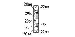
- the first slit 22ac has a first semicircular portion 22ae at the open end side (one side edge 22af side of the first slit 22ac) of the first slit 22ac, the width dimension of the first slit 22ac increases with distance from the first comb portion 22ab.
- the second slit 22bc is a second semicircular portion whose width dimension increases with distance from the second comb-tooth portion 22bb on the open end side (one side edge 22bf side of the second slit 22bc) of the second slit 22bc. It has 22be.
- the insulating layer 23 is the 4th through-hole 23be connected to the circular 3rd through-hole 23ae (refer FIG.8 (b)) connected to 1st semicircle-shaped part 22ae, and 2nd semicircle-shaped part 22be. (See FIG. 8 (b)).
- the heat transfer plate 21 has a fifth through hole 21 ae (see FIGS. 5 and 6) communicating with the first semicircular portion 22 ae via the third through hole 23 ae and a fourth through hole 23 be.
- a sixth through hole 21be (see FIGS. 5 and 6) communicating with the two semicircular portions 22be is provided.
- the first slit 22ac may have a wedge-shaped or quadrangular first wide portion in addition to the first semicircular portion 22ae on the open end side of the first slit 22ac. The first wide portion becomes wider as it is separated from the first comb-tooth portion 22ab.
- the second slit 22bc may have a wedge-shaped or square-shaped second wide portion in addition to the second semicircular portion 22be on the open end side of the second slit 22bc. The second wide portion becomes wider as it is separated from the second comb-tooth portion 22bb.
- the dimension between the one side edge 22 af of the first comb bone portion 22 aa and the one side edge 22 bf of the second comb bone portion 22 ba is smaller than the dimension of the heat transfer plate 21 in the short direction.
- the wiring pattern 22 is preferably formed smaller than the heat transfer portion 20 in the width direction of the mounting substrate 2.
- the wiring pattern 22 is disposed so as not to protrude from the heat transfer portion 20 in the width direction.
- the center in the width direction of the wiring pattern 22 and the center in the width direction of the heat transfer portion 20 are arranged to coincide with each other.
- the wiring pattern 22 and the heat transfer portion 20 are arranged so that the size is equal in the longitudinal direction and the end portions in the longitudinal direction coincide with each other.
- the wiring pattern 22 a plurality of (four in the example of FIG. 7) unit patterns 22 u having the first pattern 22 a and the second pattern 22 b are juxtaposed in the direction along the longitudinal direction of the heat transfer plate 21.
- the wiring pattern 22 includes four unit patterns 22u, and in each of the unit patterns 22u, nine LED chips 3 arranged along the longitudinal direction of the heat transfer plate 21 are electrically It can be connected to
- the unit pattern 22 u is formed in a long shape, and the longitudinal direction of the unit pattern 22 u coincides with the longitudinal direction of the wiring pattern 22.
- the wiring pattern 22 is a connecting piece 22h in which the second pattern 22b of one unit pattern 22u of the adjacent unit patterns 22u and the first pattern 22a of the other unit pattern 22u straddle these two unit patterns 22u. They are connected and electrically connected by a third connecting portion 22c (see FIG. 6B) and the later-described. That is, in the first embodiment, the unit pattern 22u is defined as a pattern sandwiched between the connecting piece 22h and the connecting piece 22h (terminal piece 22f) adjacent to the connecting piece 22h. In the connecting piece 22h, an elongated opening (slit) 22i straddling two unit patterns 22u is formed. The longitudinal direction of the opening (slit) 22 i coincides with the longitudinal direction of the heat transfer plate 21.
- the slit 22 i is provided on the side close to one end of the heat transfer plate 21 in the short direction. That is, in the wiring pattern 22, the connection piece 22h is defined as a portion on the end side of the elongated opening 22i in the width direction. The openings 22 i are elongated holes along the longitudinal direction of the wiring pattern 22. Then, the connecting piece 22h is divided in the width direction of the wiring pattern 22 to form a terminal piece 22f. Further, the opening 22i is divided in the width direction to form a slit 22ia described later. The opening 22 i is provided on the side close to one end in the width direction of the wiring pattern 22 so that the connection piece 22 h is formed to be elongated along the longitudinal direction of the wiring pattern 2. That is, the openings (slits) 22i are provided in the first comb-bone portion 22aa in a wide portion where the width dimension is wider than other portions.
- the wiring pattern 22 may be formed by one unit pattern 22 u. That is, an example of the wiring pattern 22 does not include the connecting piece 22h, and one unit pattern 22u, a terminal piece (first terminal piece) extending from the first pattern 22a of the unit pattern 22u, and the unit pattern 22u. And a terminal piece (second terminal piece) extending from the second pattern 22b. At this time, the terminal strip (first terminal strip) 22f extending from the first pattern 22a is disposed at one of both ends in the longitudinal direction of the unit pattern 22u, and extends from the second pattern 22b (second terminal A piece 22f is disposed on the other side.
- the mounting substrate 2 is provided with terminal pieces 22f at each of both end portions in the longitudinal direction. That is, the mounting substrate 2 is provided with the terminal piece 22f at the end in the longitudinal direction.
- the mounting substrate 2 includes terminal pieces (first terminal pieces) 22f extending from the first pattern 22a at one of both end portions in the longitudinal direction, and terminal pieces extending from the second pattern 22b at the other. (Second terminal strip) 22f is provided.
- the wiring pattern 22 is formed with a slit 22 ia for opening an end of the wiring pattern 22 in the longitudinal direction.
- the slits 22 ia are elongated along the longitudinal direction of the wiring pattern 22.
- the terminal piece 22f is defined at a portion on the end side of the wiring pattern 22 in the width direction than the slit 22ia. Therefore, the end of the terminal piece 22 f and the end of the wiring pattern 22 are formed to coincide in the longitudinal direction.
- the end of the wiring pattern 22 is disposed so as to be aligned with the end of the heat transfer portion 20. Therefore, the end of the terminal piece 22 f coincides with the end of the mounting substrate 2 in the longitudinal direction of the mounting substrate 2.
- the terminal pieces 22 f may be formed so as not to protrude from the wiring pattern 22 in the longitudinal direction of the wiring pattern 22.
- the terminal pieces 22 f may be formed so as not to protrude from the mounting substrate 2 in the longitudinal direction of the wiring pattern 22.
- the wiring pattern 22 is formed smaller than the length of the heat transfer portion 20 in the width direction, and is disposed near the center of the heat transfer portion 20 in the width direction. Therefore, the terminal pieces 22f are formed so as not to protrude from the mounting substrate 2 also in the width direction.
- the terminal piece 22f is formed at the end of the wiring pattern 22 in the longitudinal direction by forming the slit 22ia so as to open the end of the longitudinal direction. Therefore, if the longitudinal direction of the wiring pattern 22 is arranged to coincide with the longitudinal direction with the heat transfer portion 20 (longitudinal direction of the mounting substrate 2), the terminal strip 22f is formed at the end portion in the longitudinal direction of the mounting substrate 2 Be done.
- the terminal strip 22f is configured by a part of the connection piece 22h by cutting the wiring pattern 22 at the boundary between adjacent unit patterns 22u.
- the terminal pieces 22 f at both end portions in the longitudinal direction are arranged in line symmetry with the center line along the short direction of the mounting substrate 2 as the symmetry line.
- the slits 22 ia may be formed in an elongated shape along the width direction of the wiring pattern 22 so as to open the end in the width direction of the wiring pattern 22.
- the terminal strip 22f is defined in the wiring pattern 22 at a portion closer to the end in the longitudinal direction than the slit 22ia.
- the terminal piece 22f is formed such that the end of the terminal piece 22f is aligned with the end of the wiring pattern 22 in the width direction.
- the terminal pieces 22f are formed so as not to protrude from the mounting substrate 2 in the width direction.
- the terminal pieces 22f are formed so as not to protrude from the mounting substrate 2 also in the longitudinal direction.
- the slits 22 ia are formed on one end side in the longitudinal direction of the wiring pattern 22 so as to narrow the terminal pieces 22 f in the width direction.
- the heat transfer portion 20 is formed with a notch 20c that exposes the terminal piece 22f. That is, the notch 20c is formed larger than the terminal piece 22f at a position overlapping the terminal piece 22f in the heat transfer portion 20 in a plan view as viewed from the thickness direction (the direction perpendicular to the sheet of FIG. 1).
- the notch 20 c is formed by cutting out the corner of the heat transfer portion 20. That is, the notch 20 c is formed by cutting one end in the width direction of the heat transfer portion 20 and one end in the longitudinal direction connected to the one end. In the first embodiment, as shown in FIG. 1, it is a rectangular space in plan view formed by cutting out the corner of the heat transfer portion 20.
- the LED module 1 includes i parallel circuits of j LED chips 3 aligned in the longitudinal direction of the mounting substrate 2 and includes a series circuit in which the i parallel circuits are connected in series. There is.
- the LED module 1 can supply power to this series circuit via the two terminal pieces 22 f of the mounting substrate 2. In short, the LED module 1 can supply power to all the LED chips 3 by supplying power between the two terminal pieces 22 f described above.
- the LED module 1 is disposed such that the first terminal piece 22 f described above faces the second terminal piece 22 f of the adjacent LED module 1. Then, the opposing first terminal piece 22 f and the second terminal piece 22 f are electrically connected by the conductive member 4.
- the insulating layer 23 is formed by thermosetting an epoxy resin layer of a thermosetting sheet-like adhesive in which an B-stage epoxy resin layer (thermosetting resin) and two plastic films are laminated. . Two plastic films are laminated one by one on both sides in the thickness direction of the B-stage epoxy resin layer. Each plastic film is a PET film.
- the B-staged epoxy resin contains a filler made of a filler (second filler) such as silica or alumina, and has a property of lowering viscosity and increasing fluidity at the time of heating.
- a filler such as silica or alumina
- an insulating material having a thermal conductivity higher than that of an epoxy resin which is a thermosetting resin may be used.
- adhesive agent sheet TSA by Toray Industries, Inc. etc. are employable, for example.
- the epoxy resin layer of the sheet-like adhesive has properties such as electrical insulation, high thermal conductivity, high fluidity at the time of heating, and high adhesion to the uneven surface. Therefore, the occurrence of a gap between the insulating layer 23 and the heat transfer plate 21 and the wiring pattern 22 can be suppressed, and the adhesion reliability is improved, and the increase in thermal resistance and the occurrence of variation due to the lack of adhesion can be achieved. It becomes possible to suppress. As a result, the mounting substrate 2 has thermal resistance from the heat transfer plate 21 as compared with the case where a heat sheet such as a rubber sheet such as a rcone (registered trademark) is sandwiched between the heat transfer plate 21 and the wiring pattern 22.
- the thickness of the above-mentioned epoxy resin layer is set to 100 ⁇ m, but this value is an example and is not particularly limited. For example, it may be appropriately set in the range of about 50 ⁇ m to 150 ⁇ m. In addition, it is preferable that the heat conductivity of the above-mentioned epoxy resin layer is 4 W / m * K or more.
- the plastic film of the sheet adhesive is peeled off from the epoxy resin layer before the heat transfer plate 21 and the wiring member 222 which is the basis of the wiring pattern 22 are superposed.
- one plastic film in the epoxy resin layer is peeled off, one surface opposite to the other plastic film is fixed to the object, and then the other plastic film is peeled off.
- pressure may be appropriately applied in a state where the heat transfer plate 21, the epoxy resin layer, and the wiring member 222 are superimposed.
- the outer size of the insulating layer 23 may be appropriately set based on the outer size of the wiring member 222.
- the insulating layer 23 has electrical insulation and thermal conductivity, and has a function of electrically insulating the heat transfer plate 21 and the wiring pattern 22 and a function of thermally coupling.
- a surface treatment layer (not shown) is preferably formed on the wiring pattern 22.
- the surface treatment layer is preferably made of a metal material having high oxidation resistance and corrosion resistance as compared to the second metal plate.
- the surface treatment layer is preferably made of a metal material having high adhesion to the insulating layer 23.
- the surface treatment layer may be, for example, a Ni film, a laminated film of Ni film and Au film, a laminated film of Ni film, Pd film and Au film, Ni film and Pd film It is preferable to form a laminated film of
- the surface treatment layer is more preferably a laminated film of a Ni film and a Pd film from the viewpoint of cost reduction.
- the surface treatment layer may be formed, for example, by plating.
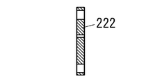
- the wiring member 222 has a first pattern 22a and a second pattern 22b.
- the wiring member 222 further includes a first connecting portion 22ad closing the first slit 22ac at the one side edge side of the first comb bone portion 22aa, and a second slit 22bc at the one side edge side of the second comb bone portion 22ba.
- a closed second connecting portion 22bd and a third connecting portion 22c connecting the first pattern 22a and the second pattern 22b are provided.
- the first pattern 22a and the second pattern 22b are not completely separated, and can be handled as one member (continuous body).
- the wiring member 222 is provided with a plurality of holes 22e for positioning with the heat transfer plate 21, and the plurality of positioning holes 22e for positioning are in the longitudinal direction of the wiring member 222 (longitudinal direction of the mounting substrate 2; Direction) are formed at equal intervals. Further, in the first step, in forming the wiring member 222, it is preferable to form the terminal piece 22f at one end in the width direction at the end of the wiring member 222 in the longitudinal direction (corner of the wiring member 222).
- the second metal plate is punched by a press to form the wiring member 222, and the longitudinal end of the wiring member 222 (second metal plate) is opened to extend along the longitudinal direction.
- the terminal piece 22f in the wiring member 222 by forming the slit 22ia having a long and narrow shape.
- the terminal piece 22 f may be formed on the wiring member 222 between the first process and the second process.
- the longitudinal direction and the width direction of the second metal plate (wiring member 222) coincide with the longitudinal direction and the width direction of the wiring pattern 22, respectively.
- connection piece 22h can be formed in the second metal plate (wiring member 222). And if a 2nd metal plate (wiring member 222) is cut
- the cutting of the connecting piece 22h may be performed in the first step, or may be performed in the second step, the third step, and the fourth step after the first step.
- a second step of temporarily bonding the heat transfer plate 21 (see FIG. 8A) and the wiring member 222 (see FIG. 8C) is performed.
- an insulating sheet 223 (see FIG. 8B) made of the above-mentioned B-stage epoxy resin layer, which is the source of the insulating layer 23, is interposed between the heat transfer plate 21 and the wiring member 222.
- the insulating sheet 223 is heated at a specified temperature (for example, 80 ° C. to 100 ° C.) lower than the curing temperature of the insulating sheet 223 to heat the heat transfer plate 21 and the wiring member 222 Are temporarily bonded to obtain the structure shown in FIG. That is, in the first embodiment, the insulating sheet 223 disposed between the heat transfer plate 21 and the wiring member 222 is heated at a temperature (specified temperature) lower than the curing temperature of the insulating sheet 223, and the heat transfer plate 21 and the wiring member 222 Bonding is called temporary bonding.
- a specified temperature for example, 80 ° C. to 100 ° C.
- the heat transfer plate 21 In the second step, it is preferable to form in the heat transfer plate 21 a notch 21 c that constitutes a part of the notch 20 c of the heat transfer section 20. Further, it is preferable to form in the insulating sheet 223 a notch corresponding to the notch portion 23 c of the insulating layer 23 which constitutes a part of the notch portion 20 c of the heat transfer section 20.
- the heat transfer plate 21 provided with the notches 21c forming the notches 20c may be used, and the insulating sheet 223 provided with notches corresponding to the notches 23c may be used.
- the third step of forming the wiring pattern 22 from the wiring member 222 is performed.
- the first connection portion 22ad, the second connection portion 22bd and the third connection portion 22c of the wiring member 222 are stamped out by a press to form the wiring pattern 22.
- the first semicircular portion 22ae of the first slit 22ac is formed in the portion of the first connecting portion 22ad by this punching process, and the second connecting portion 22bd is formed with the first semicircular portion 22ae of the first slit 22ac.
- the two semicircular portions 22be are formed, and the first pattern 22a and the second pattern 22b are separated at the third connection portion 22c.
- the connection piece 22 h may be cut to form the terminal piece 22 f at the same time as forming the wiring pattern 22 from the wiring member 222.
- the fourth step of forming the insulating layer 23 is performed to obtain the mounting substrate 2 having the structure shown in FIG.
- the insulating sheet 223 is heated and cured at a temperature (for example, 150 ° C. to 170 ° C.) higher than the curing temperature to form the insulating layer 23 for the main bonding of the heat transfer plate 21 and the wiring pattern 22.
- a temperature for example, 150 ° C. to 170 ° C.
- the insulating layer 23 is formed between the heat transfer plate 21 and the wiring member 222 by curing at a temperature higher than the curing temperature of the insulating sheet 223 and the heat transfer plate 21 and the wiring member 222 are joined. It is called this junction.
- connection piece 22h may be cut to form the terminal piece 22f.
- the mounting substrate 2 is cut after the fourth step, the mounting substrate 2 is obtained in a desired size by cutting the mounting substrate 2 along the width direction at the position of the connection piece 22h.
- the terminal strip 22f can be formed.
- the terminal piece 22 f is formed at one end of the mounting substrate 2 in the longitudinal direction.
- the insulating sheet 223 is heated at a specified temperature lower than the curing temperature of the insulating sheet 223 in the second step to temporarily bond the heat transfer plate 21 and the wiring member 222. It is possible to suppress the occurrence of warpage when the temperature is lowered in two steps. Further, in the method of manufacturing the mounting substrate 2, when the main bonding is performed in the fourth step, the first pattern 22 a and the second pattern 22 b are separated, so that the warpage occurs when the temperature is lowered. It is possible to suppress the problem. Therefore, in the method of manufacturing the mounting substrate 2, it is possible to improve the heat dissipation and manufacture the mounting substrate 2 capable of suppressing the warpage.
- the workability of the second step is improved.
- each region to be overlapped with the first connecting portion 22ad, the second connecting portion 22bd, and the third connecting portion 22c is included as the heat transfer plate 21 before the second step. It is preferable to prepare one in which each specific region to be formed is punched out by a press to form the fifth through holes 21 ae, the sixth through holes 21 be, and the seventh through holes 21 ce. Here, it is preferable that positioning holes (pilot holes) 21p at the time of processing be formed in the heat transfer plate 21 before punching processing by a press.
- each region to be overlapped with the first connecting portion 22ad, the second connecting portion 22bd, and the third connecting portion 22c is used as the insulating sheet 223 before the second step. It is preferable to prepare one in which the third through holes 23 ae, the fourth through holes 23 be, and the eighth through holes 23 ce are formed by punching out each specific region to be contained.
- the wiring member 222 can be punched by the press in the third step by preparing the heat transfer plate 21 and the insulating sheet 223 prior to the second step. You only need to punch out. Thereby, in the method of manufacturing the mounting substrate 2, it is possible to prevent short circuit between the heat transfer plate 21 and the wiring pattern 22 due to generation of burrs when punching processing is performed by a press in the third step. .
- the LED chip 3 has a first electrode (not shown) which is an anode electrode and a second electrode which is a cathode electrode on one side in the thickness direction of the LED chip 3 (the side far from the heat transfer portion 20 in the LED chip 3). An electrode (not shown) is provided.
- the LED chip 3 includes an LED structure having an n-type semiconductor layer, a light emitting layer and a p-type semiconductor layer on the main surface side of the substrate.
- the stacking order of the n-type semiconductor layer, the light emitting layer and the p-type semiconductor layer is, in order from the side close to the substrate, an n-type semiconductor layer, a light emitting layer and a p-type semiconductor layer.
- the light emitting layer may be in the order of the n-type semiconductor layer.
- the LED chip 3 more preferably has a structure in which a buffer layer is provided between the LED structure and the substrate.
- the light emitting layer preferably has a single quantum well structure or a multiple quantum well structure, but is not limited thereto.
- the n-type semiconductor layer, the light emitting layer, and the p-type semiconductor layer may form a double hetero structure.
- the structure of the LED chip 3 is not particularly limited.
- an LED chip provided with a reflective layer such as a Bragg reflector inside can also be adopted.
- the LED chip 3 is bonded to the heat transfer plate 21 via the bonding portion 35 on the other surface side ((the side closer to the heat transfer portion 20 in the LED chip 3; the lower side in FIG. It is done.
- each of the first electrode and the second electrode is electrically connected to the wiring pattern 22 through the wire 26.
- the heat transfer plate 21 is formed with the above-described first through holes 21 b through which each of the wires 26 can be passed.
- the first through holes 21 b are formed on both sides of the mounting area of each LED chip 3 in the longitudinal direction of the heat transfer plate 21.
- the bonding portion 35 can be formed of a die bonding material.
- the LED chip 3 is a GaN-based blue LED chip that emits blue light, and uses a substrate provided with a sapphire substrate.
- the substrate of the LED chip 3 is not limited to the sapphire substrate, and may be, for example, a GaN substrate, a SiC substrate, a Si substrate, or the like.
- the chip size of the LED chip 3 is not particularly limited.
- the LED chip 3 for example, one having a chip size of 0.3 mm ⁇ (0.3 mm ⁇ 0.3 mm), 0.45 mm ⁇ or 1 mm ⁇ can be used.
- the planar shape of the LED chip 3 is not limited to the square shape, and may be, for example, a rectangular shape. When the planar shape of the LED chip 3 is rectangular, for example, the chip size of the LED chip 3 can be 0.5 mm ⁇ 0.24 mm.
- the LED chip 3 does not specifically limit the material and luminescent color of a light emitting layer. That is, the LED chip 3 is not limited to the blue LED chip, and for example, a violet light LED chip, an ultraviolet light LED chip, a red LED chip, a green LED chip, or the like may be used.
- the die bonding material for example, a silicone-based die bonding material, an epoxy-based die bonding material, a silver paste, or the like can be used.
- the wire 26 for example, a gold wire, an aluminum wire or the like can be used.
- the LED module 1 includes a first sealing portion 37 embedded in the through hole 20 b and sealing a portion of the wire 26 in the through hole 20 b, the LED chip 3 and the LED chip 3 of the wires 26. And a second sealing portion 36 sealing a portion between the first sealing portion 37 and the second sealing portion 37.
- the second sealing portion 36 includes a phosphor and a transparent material that are excited by the light emitted from the LED chip 3 and emit light of a longer wavelength than the LED chip 3.
- the second sealing portion 36 has a hemispherical shape.
- the second sealing portion 36 is disposed such that the optical axis of the LED chip 3 and the optical axis of the second sealing portion 36 coincide with each other.
- the LED module 1 can suppress color unevenness.
- the LED module 1 can substantially equalize the optical path length from the LED chip 3 to the surface of the second sealing portion 36 regardless of the radiation direction of the light from the LED chip 3 and further suppress color unevenness. It is possible to
- the second sealing portion 36 is not limited to the hemispherical shape, and may have, for example, a semi-elliptic spherical shape, a semi-cylindrical shape, or the like.
- the LED module 1 may have one second sealing portion 36 for each LED chip 3, but the present invention is not limited to this.
- a desired number of LED chips 3 among the plurality of LED chips 3 aligned in the longitudinal direction of the mounting substrate 2 may be covered.
- a part of surface of the 1st sealing part 37 may be exposed.
- a silicone resin is used as a transparent material of the second sealing portion 36.
- the transparent material is not limited to a silicone resin, and may be, for example, an epoxy resin, an acrylic resin, glass, an organic / inorganic hybrid material in which an organic component and an inorganic component are mixed and combined at the nm level or molecular level.
- the phosphor of the second sealing portion 36 a phosphor which is excited by the light emitted from the LED chip 3 and emits light of a longer wavelength than the LED chip 3 can be employed.
- the second sealing portion 36 includes a phosphor and a transparent material that are excited by the light emitted from the LED chip 3 and emit light of a wavelength longer than that of the LED chip 3 and constitutes a wavelength conversion portion .
- the wavelength conversion part since the above-mentioned fluorescent substance emits the light of a color different from LED chip 3, it may be called a color conversion part.
- the first sealing portion 37 is formed of a material containing, in a first resin, a filler (first filler) having a higher reflectance than that of the first resin.
- first filler a filler having a higher reflectance than that of the first resin.
- the second sealing portion 36 is formed. It is possible to further suppress the light emitted from the phosphors from being absorbed by the first sealing portion 37, the wiring pattern 22 and the like, and it is possible to achieve high output of light.
- the first resin of the first sealing portion 37 a resin having a small difference in linear expansion coefficient with the transparent material of the second sealing portion 36 is preferable, and a resin having the same linear expansion coefficient is more preferable.
- the linear expansion coefficients of the first resin and the transparent material of the LED module 1 be equal, and the smaller the difference in linear expansion coefficient, the better.
- the difference in linear expansion coefficient is more preferably zero.
- the LED module 1 can suppress the occurrence of disconnection of the wire 26.
- a silicone resin is used, but not limited to this, for example, an epoxy resin, an acrylic resin, a glass, an organic / inorganic compound in which an organic component and an inorganic component are mixed and combined at the nm level or molecular level A hybrid material or the like may be employed.
- metal oxides such as titanium dioxide (titania), a zinc oxide, an alumina, magnesium oxide, etc. are employable, for example.
- first filler boron nitride, aluminum hydroxide or the like can be employed as the first filler.
- concentration of the first filler filled in the first resin be prepared so that the reflectance of the first sealing portion 37 is 90% or more.
- the LED module 1 can obtain white light. That is, in the LED module 1, the blue light emitted from the LED chip 3 and the light emitted from the yellow phosphor are emitted through the surface of the second sealing portion 36, and white light can be obtained.
- the LED module 1 is not limited to the yellow phosphor, but may use, for example, a yellow phosphor and a red phosphor, or by using a red phosphor and a green phosphor as the phosphors of the second sealing portion 36. It is possible to enhance color rendering.
- the fluorescent substance used as a material of the 2nd sealing part 36 may use not only 1 type of yellow fluorescent substance, but 2 types of yellow fluorescent substance from which the light emission peak wavelength differs.
- the second sealing portion 36 is in contact with the heat transfer plate 21.
- the LED module 1 can dissipate not only the heat generated by the LED chip 3 but also the heat generated by the second sealing portion 36 through the heat transfer plate 21, thereby achieving high light output. It becomes possible.
- each LED module 1 After mounting each LED chip 3 on the heat transfer unit 20, the first electrode and the second electrode of each LED chip 3 and the first pattern 22 a and the second pattern 22 b of the mounting substrate 2 And are connected via the wire 26. Thereafter, each first sealing portion 37 is formed. After that, the LED module 1 is obtained by forming each second sealing portion 36.
- the LED module 1 may have a configuration in which the second sealing portion 36 does not contain a phosphor, when a desired light emission color as the LED module 1 can be obtained by the LED chip 3 alone, and the second sealing portion 36 and the first sealing portion 37 may be formed of the same transparent material.
- the length dimension is set by appropriately setting the number of unit patterns 22u of the wiring pattern 22 and setting the dimension in the longitudinal direction of the heat transfer portion 20 according to the number of unit patterns 22u. It is possible to cope with different types of varieties.
- the LED module 1 may have a configuration in which the LED chip 3 is mounted on the heat transfer unit 20 via a submount member (not shown).
- the submount member is a stress acting on the LED chip 3 due to the difference in the coefficient of linear expansion between the LED chip 3 and the heat transfer portion 20 (in particular, the difference in the coefficient of linear expansion between the LED chip 3 and the heat transfer plate 21). It is preferable to have a stress relaxation function that relieves. Thereby, the LED module 1 can relieve the stress acting on the LED chip 3 due to the difference in the linear expansion coefficient between the LED chip 3 and the heat transfer portion 20.
- the submount member preferably has a heat transfer function of transferring the heat generated by the LED chip 3 to the heat transfer portion 20.
- the submount member has a heat transfer function of causing the heat transfer unit 20 to transfer the heat generated by the LED chip 3 to a range wider than the chip size of the LED chip 3.
- the submount member is preferably formed in a rectangular plate shape having a plane size larger than the chip size of the LED chip 3.
- the LED module 1 can improve the light extraction efficiency.
- a material which has translucency and diffusivity alumina, barium sulfate, etc. are employable, for example.
- aluminum nitride, composite SiC, Si, CuW or the like can be adopted as the material of the submount member.
- the submount member may be provided, for example, with a reflective film that reflects the light emitted from the LED chip 3 on the surface on the heat transfer unit 20 side.
- a reflective film for example, Ag, AlAu, Ni or the like can be adopted.
- the material of the reflective film is not particularly limited, and may be appropriately selected according to the emission wavelength of the LED chip 3, for example.
- the submount member is electrically connected to the first electrode or the second electrode disposed on the submount member side of the LED chip 3.
- a conductor pattern to be connected may be provided, and the conductor pattern and the first pattern 22a or the second pattern 22b may be electrically connected via the wire 26.
- each LED module 1 of the light source device 10 includes the mounting substrate 2 and a plurality of LED chips 3 arranged on one surface side of the mounting substrate 2.
- the mounting substrate 2 is a heat transfer portion 20 on which a plurality of LED chips 3 are mounted on one side and a wiring pattern disposed on the other side of the heat transfer portion 20 and to which the respective LED chips 3 are electrically connected. It has 22 and. Therefore, in the light source device 10 of the present embodiment, the heat generated in each of the LED chips 3 and each of the second sealing portions 36 can be efficiently transferred in the lateral direction by the heat transfer portion 20 and dissipated. Further, it is possible to transfer heat in the thickness direction of the heat transfer portion 20 (in the direction perpendicular to the sheet of FIG. 1) and dissipate heat. Therefore, the LED module 1 can improve the heat dissipation, can suppress the temperature rise of each LED chip 3, and can achieve high output of light output.
- the terminals of the wiring patterns 22 of the mounting substrate 2 in each LED module 1 enable the LED modules 1 to be electrically connected to each other at one end in the width direction at both ends in the longitudinal direction of the mounting substrate 2 It has a piece 22f.
- the heat transfer portion 20 of the mounting substrate 2 is formed with notches 20 c at one end side in the width direction at both end portions in the longitudinal direction of the mounting substrate 2 so as to expose the terminal piece 22 f. Then, the LED modules 1 adjacent to each other in the light source device 10 are plastically deformed so that the conductive members 4 disposed so as to cover both of the opposing terminal pieces 22f so as to hold both the terminal pieces 22f. Connected.
- the light source device 10 of the present embodiment can increase the light output.
- the heat transfer portion 20 is configured by the heat transfer plate 21 and the insulating layer 23. Therefore, the heat transfer plate 21 is formed with the notch 21c at one end side in the width direction at both ends in the longitudinal direction of the mounting substrate 2 and the insulating layer 23 is in the longitudinal direction of the mounting substrate 2 Notches 23c for exposing the terminal pieces 22f are formed at one end side in the width direction at both ends.
- the notch 21 c of the heat transfer plate 21 and the notch 23 c of the insulating layer 23 constitute a notch 20 c of the heat transfer portion 20.
- the light source device 10 uses a plurality of (two in the example of FIG. 1) LED modules 1 arranged in a straight line. That is, in the first embodiment, the light source device 10 arranges the LED modules 1 along the specified direction (longitudinal direction of the mounting substrate 2). At this time, the LED modules 1 are adjacent to each other such that the end portions in the width direction of the adjacent LED modules 1 are in the same straight line. Then, the LED modules 1 can be adjacent to each other so that the end portions in the width direction of the terminal pieces 22 f are aligned in a straight line. At this time, the terminal pieces 22f face each other in the longitudinal direction. Then, the terminal pieces 22f of the adjacent LED modules 1 are electrically connected by the conductive member 4 and mechanically connected. As a result, the light source device 10 can supply power from one power supply unit to the series circuit of the plurality of LED modules 1 to make all the LED chips 3 of each LED module 1 emit light.
- the conductive member 4 is preferably one that can be disposed so as to cover both of the opposing terminal pieces 22f and can be plastically deformed.
- a material of such a conductive member 4 aluminum, copper etc. are preferable, for example.
- the conductive member 4 can be plastically deformed so as to hold the two terminal pieces 22f, thereby electrically connecting the two terminal pieces 22f. That is, both the terminal pieces 22 f can be electrically and mechanically connected by the conductive member 4.
- a cylindrical (cylindrical in the illustrated example) member as shown in FIG. 10 can be used. The arrow in FIG. 10 indicates the insertion direction of the terminal piece 22 f into the cylindrical conductive member 4.
- FIG. 3 is a cross-sectional view of the light source device 10 after plastic deformation of the conductive member 4.
- the conductive member 4 When the conductive member 4 is plastically deformed, the conductive member 4 may be plastically deformed using, for example, a caulking tool or a caulking chisel. In short, in order to connect the two terminal pieces 22f electrically and mechanically, the conductive member 4 is disposed so as to cover the two terminal pieces 22f, and then the conductive member 4 is crimped. The member 4 may be plastically deformed. In the light source device 10, when the terminal pieces 22f are electrically and mechanically connected by the conductive member 4 as described above, a connecting device such as a connector is not necessary, and heating of solder or the like is necessary. It is not necessary to use a bonding material.
- the electrically conductive members 4 electrically and mechanically connect terminal pieces 22f exposed by the notched portion 20c at one end side in the width direction at both end portions in the longitudinal direction of the mounting substrate 2 of adjacent LED modules 1 Since it is connected to, when viewed as a line light source, it is possible to suppress a change in the distance between the LED chips 3 halfway in the longitudinal direction. In addition, since the light source device 10 can make the distance between the LED chips 3 constant without lengthening the arrangement pitch of the LED chips 3 in the LED module 1, the individual LED chips 3 become granular as point light sources. It becomes possible to suppress that it looks like it is shining.
- the light source device 10 it is possible to suppress that a part of light emitted from the LED chip 3 is blocked or absorbed by the conductive member 4, and it is possible to suppress a decrease in light output. It becomes.
- the light source device 10 is a conductive member (second conductive member) 5 in which the terminal piece 22 f (terminal piece 22 fp) and the lead wire 6 which is a wire are both covered at both ends in the specified direction. Are preferably plastically deformed and electrically connected so as to hold the two.
- the second conductive member 5 may cover the conductor portion 6 b exposed by peeling off a part of the insulation coating of the lead wire 6. That is, among the terminal pieces 22 f, the terminal pieces 22 fp not connected to the terminal pieces 22 f of the other LED modules 1 are electrically connected to the lead wire 6.
- a terminal piece 22fp that is located at an end in the above-mentioned prescribed direction and does not face the other terminal piece 22f is electrically connected to the lead wire 6.
- a connection device such as a connector is unnecessary, and It is not necessary to use a bonding material that requires heating, such as solder.
- the second conductive member 5 one having the same shape as the conductive member 4 can be employed, which makes it possible to achieve cost reduction by commonality of parts.
- the heat generated in each of the LED chips 3 and each of the second sealing portions 36 of the LED module 1 is dissipated through the heat transfer plate 21 formed using the first metal plate. Therefore, even if the light output of each LED module 1 is increased by increasing the light output of each LED chip 3 or the like, for example, each light emitting diode chip 3 and each second sealing portion It becomes possible to suppress the temperature rise of 36, and it becomes possible to attain high output of light output.
- the LED chip 3 Since the insulating layer 23 of the LED module 1 contains a filler (second filler) having a thermal conductivity higher than that of the thermosetting resin in the thermosetting resin, the LED chip 3 It is possible to more efficiently dissipate the heat generated in the
- the light source device 10 Since the light source device 10 includes the heat transfer plate 21 and the wiring pattern 22 formed using the second metal plate, the light source device 10 uses the LED chip 3 mounted on a metal base printed wiring board. In comparison, it is possible to achieve high output of light output at low cost. Moreover, by using the light source device 10 having a function as a reflection plate as the heat transfer plate 21 of the LED module 1, it becomes possible to reduce the light loss in the heat transfer plate 21 and the light output is high. It becomes possible to achieve output. Therefore, the light source device 10 can also achieve low power consumption.
- the first metal plate of the heat transfer plate 21 is the aluminum plate 98, and the aluminum film 99 higher in purity than the aluminum plate 98 is stacked on the aluminum plate 98 on the opposite side to the insulating layer 23 side.
- the light source device 10 can efficiently dissipate the heat generated by the LED chip 3 to increase the light output, and further, improve the utilization efficiency of the light emitted from the LED chip 3 It is possible to Further, the light source device 10 transfers heat of light emitted from the phosphor as a wavelength conversion material to the heat transfer plate 21 side, light emitted from the LED chip 3 and scattered to the heat transfer plate 21 by the phosphor, and the like. Since the light can be reflected by the portion 20, it is possible to improve the utilization efficiency of light.
- the first pattern 22a and the second pattern 22b of the wiring pattern 22 on the mounting substrate 2 of the LED module 1 are respectively formed in a comb shape and arranged so as to be intertwined with each other.
- the first pattern 22a one side edge side opposite to the second comb bone portion 22ba in the first comb bone portion 22aa is opened, and a first slit 22ac reaching the first comb tooth portion 22ab is formed.
- the second pattern 22b is formed with a second slit 22bc which is open at one side edge side opposite to the first comb bone portion 22aa side in the second comb bone portion 22ba and extends to the second comb tooth portion 22bb.
- the LED module 1 can improve the heat dissipation and suppress the warpage. Therefore, the light source device 10 can improve the heat dissipation and can suppress the warpage.
- the heat transfer plate 20 of the LED module 1 is formed of the first metal plate, and the long heat transfer plate 21 on which the LED chips 3 are mounted on one side; And an insulating layer 23 disposed on the other side and having electrical insulation and thermal conductivity.
- the heat transfer property can be further improved by forming the heat transfer plate 21 of the LED module 1 by the first metal plate, and an insulating layer having electrical insulation and thermal conductivity.
- the provision of the reference numeral 23 makes it possible not only to electrically insulate the heat transfer plate 21 and the wiring pattern 22 but also to improve the heat dissipation.
- each LED module 1 of the light source device 10 has a plurality of LED chips 3 mounted on the mounting substrate 2, the mounting substrate 2 has the above-described insulating layer 23 between the heat transfer plate 21 and the wiring pattern 22
- the thermal resistance from each LED chip 3 to the wiring pattern 22 is greater than in the case where a heat-radiating sheet or the like in the form of a rubber sheet such as Sarcon (registered trademark) is sandwiched between the heat transfer plate 21 and the wiring pattern 22. While being able to reduce, it becomes possible to reduce the variation in thermal resistance. As a result, in the light source device 10, the heat dissipation of each LED module 1 is improved, and the temperature rise of the junction temperature of each LED chip 3 can be suppressed, so that the input power can be increased. It is possible to
- FIG. 11A a member or the like in which a sheet metal is bent in a U-shape can be used. That is, in FIG. 11A, the cross-sectional shape of the conductive member 4 is U-shaped.
- the arrow in FIG. 11 (a) has shown the direction to which the electroconductive member 4 is moved so that the terminal piece 22f of adjacent LED module 1 may be covered.
- FIG. 11B is a cross-sectional view of the light source device 10 after plastic deformation of the conductive member 4. That is, in the case where the U-shaped conductive member 4 is used, the LED modules 1 are arranged along the specified direction (longitudinal direction of the mounting substrate 2).
- the conductive member 4 is brought close to the terminal piece 22 f of the adjacent LED module 1 from the U-shaped opening portion, and the terminal piece 22 f of the adjacent LED module 1 is inserted into the U-shaped inner side of the conductive member 4.
- each of the terminal pieces 22f is wrapped with the conductive member 4 so as to cover each of the terminal pieces 22f of the adjacent LED modules 1. It is fixed in the contact state.
- the terminal pieces 22 f of the adjacent LED modules 1 are electrically connected via the conductive member 4. That is, adjacent LED modules 1 are electrically connected.
- the terminal strip 22fp and the lead wire 6 are placed inside the U-shape of the conductive member 4, and the conductive member 4 is opened in the U-shape.
- the terminal piece 22fp and the lead wire 6 can be electrically connected by plastic deformation so as to reduce.
- the conductive member 4 of FIG. 11 is U-shaped, the position where the conductive member 4 covers both the terminal pieces 22f from the side of the LED module 1 in a state where the LED modules 1 are butted. It is possible to move up to.
- the conductive member 4 (second conductive member 5) is preferably in a tubular shape.
- the terminal piece 22 f of the LED module 1 may be inserted into each of the facing openings of the cylindrical conductive member 4.
- the terminal strip 22fp and the lead wire 6 may be inserted into the opposed openings of the second conductive member 5, respectively. Then, when the terminal piece 22fp and the lead wire 6 are inserted into the cylindrical second conductive member 5 and the second conductive member 5 is plastically deformed so that the diameter direction of the cylindrical becomes smaller, the second The conductive member 5 is fixed in contact with the terminal piece 22fp and the lead wire 6. Then, the LED module 1 and the lead wire 6 are electrically connected.
- the terminal piece 22f of the light source device 10 may have a hole 22fa as shown in FIG. 12 (a).
- the light source device 10 has a structure in which a part of the plastically deformed conductive member 4 (second conductive member 5) has entered the hole 22fa. Then, the plastically deformed conductive member 4 (second conductive member 5) can be caught in the hole 22fa.
- the light source device 10 can improve the reliability of the mechanical connection between the two terminal pieces 22 f by the conductive member 4.
- the reliability of the mechanical connection between the terminal strip 22fp and the lead wire 6 by the second conductive member 5 can be improved.
- hole 22fa of the terminal piece 22f in FIG. 12 (a), (b) is a through-hole penetrated in the thickness direction of the terminal piece 22f, it is not restricted to this and the hollow which is not penetrating may be sufficient.
- the terminal piece 22f of the light source device 10 may be formed with a notch 22fb as shown in FIG.
- the light source device 10 has a structure in which a part of the plastically deformed conductive member 4 enters the notch 22fb. Then, the plastically deformed conductive member 4 (second conductive member 5) can be caught by the notch 22fb. Thereby, the light source device 10 can improve the reliability of the mechanical connection between the two terminal pieces 22 f by the conductive member 4.
- the notch 22fb is formed at the end of the terminal piece 22f in the longitudinal direction.
- the notch 22fb is formed at the end portion on the center side of the wiring pattern 22 of both end portions in the longitudinal direction of the terminal piece 22f.
- the conductive member 4 of the light source device 10 may have a recess 4 b that is recessed relative to the other portion of the conductive member 4.
- the recess 4b is, for example, formed in a portion corresponding to the hole 22fa of the terminal piece 22f in FIG. 12 (b) or in a portion corresponding to the notch 22fb of the terminal piece 22f in FIG. 13 (b).
- the conductive member 4 (the second conductive member 5) is disposed in the light source device 10 such that the recess 4b is recessed in the thickness direction of the mounting substrate 2 (the direction perpendicular to the sheet of FIG. 1).
- both terminal pieces 22f connected by the conductive member 4 are, as shown in FIG. 15, along the thickness direction of the wiring pattern 22 (vertical direction in FIG. 1) toward the notch 20c. It may be bent. Arrows in FIG. 15 indicate directions in which the conductive members 4 are moved so as to cover the terminal pieces 22 f of the adjacent LED modules 1.
- the cylindrical conductive member 4 is moved from the one surface (the first surface 20m) side of the heat transfer portion 20 to cover both the terminal pieces 22f. It is also possible to prevent the conductive member 4 from falling off before plastically deforming the conductive member 4, so that the assemblability of the light source device 10 can be improved.
- the hole 22fa or the notch 22fb may be provided in the terminal strip 22f in FIG.
- the light source device 10 having the bent terminal piece 22f may adopt the U-shaped conductive member 4 instead of the cylindrical conductive member 4 in FIG.
- the light source device 10 is a light source device 10 in which a plurality of LED modules 1 are arranged in a specified direction and adjacent LED modules 1 are electrically connected to each other.
- the LED module 1 includes the long mounting substrate 2 and the plurality of LED chips 3 arranged along the longitudinal direction of the mounting substrate 2.
- the mounting substrate 2 is formed of a long heat transfer portion 20 on which each LED chip 3 is mounted on one side and a conductive plate and is disposed on the other surface side of the heat transfer portion 20, and each LED chip 3 is electrically And a wiring pattern 22 connected in an orderly manner.
- the wiring pattern 22 has terminal pieces 22 f that enable the LED modules 1 to be electrically connected to each other at one end side in the width direction at both end portions in the longitudinal direction of the mounting substrate 2.
- the heat transfer portion 20 is formed with notches 20 c at one end side in the width direction at both end portions in the longitudinal direction of the mounting substrate 2 so as to expose the terminal piece 22 f.
- the LED modules 1 are electrically connected such that the conductive members 4 disposed so as to cover both of the opposing terminal pieces 22f are plastically deformed so as to hold the terminal pieces 22f.
- the conductive member 4 is preferably a cylindrical member.
- the conductive member 4 is preferably a member in which a sheet metal is bent in a U-shape.
- the terminal piece 22f preferably has a hole 22fa or a notch 22fb in which a part of the plastically deformed conductive member 4 is inserted.
- the conductive member 4 preferably has a recess 4 b that is recessed relative to other portions of the conductive member 4.
- both of the terminal pieces 22 f connected by the conductive member 4 are preferably bent toward the notch 20 c along the thickness direction of the wiring pattern 22.
- the second conductive member 5 in which the terminal piece 22fp and the lead wire 6 are disposed so as to cover both hold plastically. It is preferable to be deformed and electrically connected.
- the heat transfer unit 20 is formed of the first metal plate and is disposed on the other surface side of the heat transfer plate 21 and the heat transfer plate 21 on which each LED chip 3 can be mounted.
- the conductive plate preferably has the same coefficient of linear expansion as that of the heat transfer plate 21, but the conductive plate may be different from the heat transfer plate 21.
- the insulating layer 23 preferably contains a filler having a thermal conductivity higher than that of the thermosetting resin in the thermosetting resin.
- the first metal plate is the aluminum plate 98, and the aluminum film 99 of higher purity than the aluminum plate 98 on the opposite side of the aluminum plate 98 to the insulating layer 23 side. It is preferable that the reflective film 100 be formed by laminating the aluminum film 99 and at least two types of dielectric films 101 and 102 having different refractive indexes.
- the light source device 10 includes a wavelength conversion unit including a phosphor and a transparent material which is excited by light emitted from the LED chip 3 and emits light having a wavelength longer than that of the LED chip 3;
- the portion is preferably in contact with the heat transfer portion 20.
- each LED chip 3 is provided with the first electrode and the second electrode on one surface side in the thickness direction, and each of the first electrode and the second electrode is a wire.
- the heat transfer portion 20 is preferably electrically connected to the wiring pattern 22 through the through holes 26, and the heat transfer portion 20 is preferably formed with through holes 20b through which the respective wires 26 pass.
- the light source device 10 is the light source device 10 in which the plurality of LED modules 1 are arranged in the specified direction, and has the following first to tenth, twelfth, and thirteenth features.
- the eleventh feature will be described later.
- only the first feature may be provided, and in addition to the first feature, one or more of the second, fourth to thirteenth features may be provided. It is also good.
- one or more of the third to thirteenth features may be provided in addition to the first feature.
- each of the LED modules 1 includes an elongated mounting substrate 2 and a plurality of LED chips 3 arranged along the longitudinal direction of the mounting substrate 2.
- the mounting substrate 2 is formed of a long heat transfer portion 20 having a first surface 20 m and a second surface 20 n on which the LED chip 3 is mounted, and a conductive plate disposed on the second surface 20 n.
- the wiring pattern 22 electrically connected.
- the wiring pattern 22 has a terminal piece 22f for electrically connecting the LED modules 1 with each other, and the heat transfer portion 20 has a cutout 20c for exposing the terminal piece 22f.
- the terminal piece 22 f and the notch 20 c are disposed at one end side in the width direction at both end portions in the longitudinal direction of the mounting substrate 2.
- the LED modules 1 adjacent to each other are arranged such that their terminal pieces 22f face each other, and the conductive members 4 are arranged so as to cover the terminal pieces 22f facing each other and hold the terminal pieces 22f facing each other By being plastically deformed, they are electrically connected to each other.
- the conductive member 4 is cylindrical.
- the conductive member 4 is a member formed by bending a sheet metal in a U-shape.
- each of the terminal pieces 22f has a hole 22fa or a notch into which a part of the plastically deformed conductive member 4 is inserted.
- the conductive member 4 is provided with a recess 4 b that is recessed relative to other portions in the conductive member 4.
- the terminal piece 22f connected by the conductive member 4 is folded toward the notch 20c in the thickness direction of the wiring pattern 22. It is a song.
- the terminal piece 22fp located at the end in the predetermined direction has the second conductive member 5 at the end in the predetermined direction.
- the lead wire 6 is disposed so as to cover both of the positioned terminal piece 22fp and the lead wire 6, and is plastically deformed so as to hold the terminal piece 22fp at the end of the specified direction and the lead wire 6, Connected.
- the heat transfer portion 20 is a heat transfer comprising a surface on which the LED chip 3 is mounted and the other surface opposite to the one surface.
- the heat transfer plate 21 is formed of a first metal plate
- the conductive plate is formed of a second metal plate. The first metal plate and the second metal plate have different coefficients of linear expansion.
- the insulating layer 23 contains a thermosetting resin and a filler having a high thermal conductivity as compared to the thermosetting resin.
- the heat transfer plate 21 includes an aluminum plate 98, an aluminum film 99, and a reflection enhancing film 100 as the first metal plate.
- the aluminum film 99 is disposed on the side of the aluminum plate 98 opposite to the insulating layer 23 side.
- the reflection increasing film 100 is disposed on the aluminum film 99.
- the aluminum film 99 is higher in purity than the aluminum plate 98.
- the reflection increasing film 100 is composed of at least two types of dielectric films 101 and 102 having different refractive indexes.
- the phosphor according to any one of the first to eleventh aspects which is excited by the light emitted from the LED chip 3 and emits light having a wavelength longer than that of the LED chip 3 and a transparent
- a wavelength converter including a material is provided.
- the wavelength converter is in contact with the heat transfer unit 20.
- each LED chip 3 includes a first electrode and a second electrode on one surface in the thickness direction, and the wiring pattern 22 includes One pattern 22a and a second pattern 22b are provided.
- the first electrode is electrically connected to the first pattern 22 a through the wire 26, and the second electrode is electrically connected to the second pattern 22 b through the wire 26.
- the heat transfer unit 20 includes through holes 20 b through which each of the wires 26 passes.
- the heat dissipation can be improved, and the light output can be increased.
- the light source device 10 of the present embodiment will be described based on FIGS. 17 to 22.
- FIG. since the basic configuration of the light source device 10 of the present embodiment is substantially the same as that of the first embodiment, the same components as those of the light source device 10 of the first embodiment are denoted by the same reference numerals and the description thereof is omitted.
- the LED module 1 according to the first embodiment two through holes 20 b forming a set in the mounting substrate 2 are aligned in the longitudinal direction of the heat transfer portion 20.
- two through holes 20 b forming a set in the mounting substrate 2 are aligned in the lateral direction of the heat transfer portion 20.
- the first slit 22ac in the wiring pattern 22 of the mounting substrate 2 is one end side in the width direction of the first comb teeth 22ab than the center in the width direction of the first comb teeth 22ab. It is formed in the position which shifted to.
- the first slit 22ac of the wiring pattern 22 is formed at the center in the width direction of the first comb-tooth portion 22ab.
- transduce the wire 26 connected to 1st pattern 22a is formed so as to correspond to 1st comb part 22aa of 1st pattern 22a.
- the through hole 20b into which the wire 26 connected to the second pattern 22b can be introduced is formed to correspond to the tip of the second comb 22b.
- the second metal plate is subjected to a punching process using a press to perform a first step of forming a wiring member 222 as shown in FIG. 21C.
- the wiring member 222 has a first pattern 22a and a second pattern 22b.
- the wiring member 222 further includes a first connecting portion 22ad closing the first slit 22ac at the one side edge side of the first comb bone portion 22aa, and a second slit 22bc at the one side edge side of the second comb bone portion 22ba.
- a closed second connecting portion 22bd and a third connecting portion 22c connecting the first pattern 22a and the second pattern 22b are provided.
- the first pattern 22a and the second pattern 22b are not completely separated, and can be handled as one member (continuous body).
- the connection piece 22h may be cut in the first step to form the terminal piece 22f.
- a second step of temporarily bonding the heat transfer plate 21 (see FIG. 21A) and the wiring member 222 (see FIG. 21C) is performed.
- an insulating sheet 223 (see FIG. 21B) made of the above-mentioned B-stage epoxy resin layer, which is the source of the insulating layer 23, is interposed between the heat transfer plate 21 and the wiring member 222.
- the insulating sheet 223 is heated at a specified temperature (for example, 80 ° C. to 100 ° C.) lower than the curing temperature of the insulating sheet 223 to temporarily join the heat transfer plate 21 and the wiring member 222 as shown in FIG.
- the third step of forming the wiring pattern 22 from the wiring member 222 is performed.
- the wiring pattern 22 is formed by punching out a part of the first connection portion 22ad, the second connection portion 22bd and the third connection portion 22c of the wiring member 222 with a press.
- the first semicircular portion 22ae of the first slit 22ac is formed in the portion of the first connecting portion 22ad by this punching process
- the second connecting portion 22bd is formed with the first semicircular portion 22ae of the first slit 22ac.
- the two semicircular portions 22be are formed, and the first pattern 22a and the second pattern 22b are separated at the part of the third connection portion 22c.
- the terminal piece 22f may be formed on the wiring pattern 22 by dividing the connection piece 22h in the third step.
- the mounting substrate 2 having the structure shown in FIG. 20 is obtained by performing the fourth step of forming the insulating layer 23.
- the insulating sheet 223 is heated and cured at a temperature (for example, 150 ° C. to 170 ° C.) higher than the curing temperature to form the insulating layer 23 for the main bonding of the heat transfer plate 21 and the wiring pattern 22. Do.
- the insulating sheet 223 is heated at a specified temperature lower than the curing temperature of the insulating sheet 223 in the second step to temporarily bond the heat transfer plate 21 and the wiring member 222. It is possible to suppress the occurrence of warpage when the temperature is lowered in the second step. Further, in the method of manufacturing the mounting substrate 2 as described above, when the main bonding is performed in the fourth step, since the first pattern 22 a and the second pattern 22 b are separated, the warpage occurs when the temperature is lowered. Can be suppressed. Therefore, in the method of manufacturing the mounting substrate 2, it is possible to improve the heat dissipation and manufacture the mounting substrate 2 capable of suppressing the warpage.
- the workability of the second step is improved.
- the processability of the plating process for forming the surface treatment layer on the wiring pattern 22 is improved.
- each LED module 1 since each LED module 1 includes the above mounting substrate 2 and the LED chip 3 mounted on the mounting substrate 2, heat dissipation can be improved, and warpage can be achieved. It becomes possible to suppress. Further, as in the first embodiment, the LED module 1 is plastically deformed so that the conductive member 4 disposed so as to cover both of the opposing terminal pieces 22f to hold both the terminal pieces 22f. Connected. Thereby, the light source device 10 of the present embodiment can increase the light output.
- the light source device 10 includes the first to tenth, twelfth, and thirteenth features described above. Also in the second embodiment, the light source device 10 may have only the first feature, and in addition to the first feature, any one of the second to tenth, twelfth, and thirteenth selected. The above features may be provided.
- the basic configuration of the light source device 10 of the present embodiment is substantially the same as that of the second embodiment, so the same components as those of the light source device 10 of the second embodiment are denoted by the same reference numerals and the description thereof is omitted.
- the heat transfer plate 20 and the insulating layer 23 constitute the heat transfer unit 20.
- the heat transfer unit 20 is formed of a resin (second resin) containing a filler (third filler) and having electrical insulation. The points are different. Moreover, it is preferable that the heat transfer part 20 has diffuse reflection and is non-light transmitting.
- the heat transfer section 20 can adopt unsaturated polyester as the second resin, and can adopt titania as the filler.
- the second resin of the heat transfer portion 20 is not limited to unsaturated polyester, and, for example, vinyl ester can be adopted.
- the filler is not limited to titania, and, for example, magnesium oxide, boron nitride, aluminum hydroxide or the like can be used.
- the heat conductivity of the heat transfer portion 20 is preferably 0.5 W / m ⁇ K or more.
- the mounting substrate 2 further includes an insulating portion 28 covering the wiring pattern 22 on the other surface side of the heat transfer portion 20.
- the insulating portion 28 is preferably formed of the same material as the heat transfer portion 20.
- the conductive member 4 (second conductive member 5) may be cylindrical.
- the conductive member 4 (second conductive member 5) may be a member in which a sheet metal is bent in a U-shape.
- a hole 22fa or a notch 22fb may be formed in each of the terminal pieces 22f so that a part of the plastically deformed conductive member 4 (second conductive member 5) enters.
- the conductive member 4 (second conductive member 5) may be provided with a recess 4b which is recessed relative to other portions in the conductive member 4 (second conductive member 5).
- terminal pieces 22 f connected by the conductive member 4 may be bent toward the notch 20 c along the thickness direction of the wiring pattern 22. Furthermore, the terminal strip 22fp located at the end in the specified direction is arranged such that the second conductive member 5 covers both the terminal strip 22fp and the lead wire 6 and holds the terminal strip 22fp and the lead wire 6 May be electrically connected to the lead wire 6 by plastic deformation.
- FIGS. 27, 29, 31, and 33 are plan views, and FIGS. 28, 30, 32, and 34 are cross-sectional views taken along the line AA in FIGS. 27, 29, 31, and 33, respectively. Is listed.
- a first process of forming the wiring member 222 as shown in FIGS. 27 and 28 is performed by punching the conductive plate which is the base of the wiring pattern 22 by a press.
- the wiring member 222 has a first pattern 22a and a second pattern 22b.
- the wiring member 222 further includes a first connecting portion 22ad closing the first slit 22ac at the one side edge side of the first comb bone portion 22aa, and a second slit 22bc at the one side edge side of the second comb bone portion 22ba.
- a closed second connecting portion 22bd and a third connecting portion 22c connecting the first pattern 22a and the second pattern 22b are provided.
- the first pattern 22a and the second pattern 22b are not completely separated, and can be handled as one member (continuous body). Further, as in the method of manufacturing the mounting substrate 2 of the first embodiment, it is preferable to form the terminal piece 22 f in the wiring member 222 in the first step. Further, in the first step, the connection piece 22 h may be formed on the wiring member 222. That is, as the first step of the method of manufacturing the mounting substrate of the third embodiment, the same step as the first step of the method of manufacturing the mounting substrate of the first embodiment can be employed.
- a second step of forming the heat transfer portion 20 in which a part of the wiring member 222 is embedded is formed by an insert molding method to obtain the structure shown in FIGS.
- the heat transfer portion 20 be formed so as to include a notch 20 c that exposes the terminal piece 22 f provided in the wiring member 222 (the connection piece 22 h provided in the wiring member 222).
- the third step of forming the wiring pattern 22 from the wiring member 222 is performed to obtain the structures shown in FIGS. 31 and 32.
- the wiring pattern 22 is formed by punching out a part of the first connection portion 22ad, the second connection portion 22bd and the third connection portion 22c of the wiring member 222 with a press.
- the first semicircular portion 22ae of the first slit 22ac is formed in the portion of the first connecting portion 22ad by this punching process, and the second connecting portion 22bd is formed with the first semicircular portion 22ae of the first slit 22ac.
- the two semicircular portions 22be are formed, and the first pattern 22a and the second pattern 22b are separated at the part of the third connection portion 22c.
- the mounting substrate 2 having the structure shown in FIGS. 33 and 34 is obtained by performing the fourth step of forming the insulating portion 28 by the insert molding method. It is preferable that a notch corresponding to the notch 20 c of the heat transfer unit 20 is also formed in the insulating unit 28.
- the mounting substrate 2 With such a method of manufacturing the mounting substrate 2, it is possible to improve the heat dissipation and manufacture the mounting substrate 2 capable of suppressing warpage. Further, in the method of manufacturing the mounting substrate 2 as described above, since the first pattern 22a and the second pattern 22b are separated by punching the wiring member 222 in the third step, the workability of the second step is improved. And the processability of the plating process for forming the surface treatment layer on the wiring pattern 22 is improved.
- each LED module 1 includes the mounting substrate 2 described above and the LED chip 3 mounted on the mounting substrate 2, so that the heat dissipation can be improved, and the warpage can be reduced. It becomes possible to suppress. Further, as in the second embodiment, the LED module 1 is plastically deformed so that the conductive member 4 disposed so as to cover both of the opposing terminal pieces 22f so as to hold the both terminal pieces 22f. Connected. Thereby, the light source device 10 of the present embodiment can increase the light output.
- the mounting substrate 2 described in the third embodiment may be employed instead of the mounting substrate 2 of the LED module 1 in the first embodiment.
- each LED module 1 of the light source device 10 includes the insulating portion 28, mechanical strength can be enhanced, and insulation on the back side can be secured. . Thereby, the light source device 10 becomes easy to handle, for example, when it is incorporated as a light source of a lighting device.
- the insulating unit 28 may also be provided in the LED module 1 of the light source device 10 of the first embodiment or the second embodiment.
- the wiring pattern 22 may be the wiring pattern 22 described in the first embodiment.
- a plate-shaped molded product made of a resin containing the above-described filler and having an electrical insulating property may be used as the heat transfer portion 20.
- the heat transfer portion 20 is preferably formed of a resin containing a filler and having electrical insulation.
- the light source device 10 according to the third embodiment includes the following eleventh feature in addition to the above first feature.
- the heat transfer portion 20 is formed of a resin containing a filler and having electrical insulation.
- the light source device 10 of the third embodiment may have a second feature in addition to the first and eleventh features.
- the light source device 10 having the first, second, and eleventh features may further include one or more features arbitrarily selected from the fourth to seventh, twelfth, and thirteenth features.
- the light source device 10 of the third embodiment may have a third feature in addition to the first and eleventh features.
- the light source device 10 having the first, third, and eleventh features may further include one or more features arbitrarily selected from the fourth to seventh, twelfth, and thirteenth features.
- the light source devices 10 of the first to third embodiments can be used as light sources of various lighting devices.
- a lighting device provided with the light source device 10 for example, as shown in FIG.
- pipe type LED lamp 90 can be comprised.
- the straight tube type LED lamp 90 for example, “The straight tube type LED lamp system with L-shaped pin cap GX16t-5 (for general lighting)” (JEL 801) has been standardized by the Japan Light Bulb Industry Association ing.
- a straight tube type LED lamp 90 is configured, for example, a straight tube-like tube main body 91 formed of a translucent material (for example, milk white glass, milk white resin, etc.) and the tube main body 91
- the light source device 10 may be housed in the tube main body 91, including the first base T1 and the second base T2 provided at each of the one end and the other end in the longitudinal direction.
- the embodiment of the lighting apparatus 80 comprises the following fourteenth feature.
- the lighting fixture 80 includes a fixture main body 81 and the light source device 10.
- the light source device 10 is held by the instrument body 81.
- the light source device 10 has the first feature described above.
- the light source device 10 has one or more features arbitrarily selected from the above-described second to thirteenth features in addition to the first feature. May be
- the embodiment of the lamp 90 has the following fifteenth features.
- the lamp 90 includes a straight tubular tube body 91 and the light source device 10, and the light source device 10 is housed in the tube body 91.
- the light source device 10 has the first feature described above.
- the light source device 10 has one or more features arbitrarily selected from the above-described second to thirteenth features in addition to the first feature. It is also good.
Landscapes
- Engineering & Computer Science (AREA)
- Microelectronics & Electronic Packaging (AREA)
- Manufacturing & Machinery (AREA)
- Led Device Packages (AREA)
- Non-Portable Lighting Devices Or Systems Thereof (AREA)
- Structure Of Printed Boards (AREA)
Abstract
本発明に係る光源装置は、複数のLEDモジュールが規定方向に並べられた光源装置である。前記LEDモジュールの各々は、長尺状の実装基板と複数のLEDチップとを備える。前記実装基板は、長尺状の伝熱部と、導電板から形成されて前記LEDチップが電気的に接続される配線パターンと、を備える。前記配線パターンは、前記LEDモジュール同士を電気的に接続するための端子片を有し、前記伝熱部は、前記端子片を露出させる切欠部を有する。前記端子片と前記切欠部とは、前記実装基板の長手方向の両端部において幅方向の一端側に配置される。隣り合う前記LEDモジュール同士は、互いの前記端子片が対向するように配置され、かつ、導電性部材が対向する前記端子片同士を覆うように配置され対向する前記端子片同士を保持するように塑性変形されることにより、互いに電気的に接続される。
Description
本発明は、光源装置に関するものである。
従来から、例えば文献1(日本国公開特許公報第2010-98302号)に示すように、複数の発光モジュールを一列に並べることによってライン光源を構成する発光装置が知られている。
文献1には、例えば、図37に示すように、同一の構造を有した発光モジュール101を点対称に配置して互いに接続することで構成される発光装置125が提案されている。各発光モジュール101は、基板102と、複数の発光ダイオード111と、連結コネクタ115と、端部コネクタ121とを備えている。
基板102は、図38および図39に示すように、長方形である。基板102は、絶縁材(例えば、ガラスエポキシ樹脂)を主体として形成されている。基板102は、発光面となる表面に、発光ダイオード111を直列接続した回路を有している。また、この回路は、白色系の被膜からなる絶縁被膜で覆われている。回路は、図38に示すように、第1の導体パターン103と、第2の導体パターン104と、複数の第3の導体パターン105と、第4の導体パターン106により形成されている。各導体パターン103、104、105、106は、銅箔などの金属で構成されている。
第1の導体パターン103と第2の導体パターン104は、基板102の長手方向の両端部にそれぞれ設けられている。複数の第3の導体パターン105は、第1の導体パターン103と第2の導体パターン104との間で基板102の長手方向に沿って並べて設けられている。第4の導体パターン106は、第1の導体パターン103が設けられた側から第2の導体パターン104が設けられた側までにわたるように基板102の長辺に沿って設けられている。
第4の導体パターン106の一端部106aは、基板102の短辺に沿って第1の導体パターン103に並んでいる。第4の導体パターン106の他端部106bは、基板102の短辺に沿って第2の導体パターン104に並んでいる。第1の導体パターン103~第3の導体パターン105は、ヒートスプレッダとして機能できるようにするために基板102上でなるべく広い面積を確保している。
また、基板102は、裏面に、その略全域にわたって広がる金属箔107が設けられている。金属箔107は、銅箔などからなり、絶縁被膜で覆われている。
連結コネクタ115は、基板102の長手方向の一端部で幅方向の中央に位置し、基板102の表面に実装されている。
端部コネクタ121は、基板102の長手方向の他端部で幅方向の中央に位置し、基板102の表面に実装されている。
端部コネクタ121は、図38に示すように、短絡片131または電源線135が接続される。短絡片131および電源線135は、いずれも絶縁被覆電線である。図37の発光装置125では、一対の発光モジュール101の連結コネクタ115どうしが接続され、一方の発光モジュール101の端部コネクタ121に短絡片131が差し込み接続され、他方の発光モジュール101の端部コネクタ121に電源線135が差し込み接続されている。
上述の発光モジュール101や発光装置125では、発光ダイオード111で発生した熱が、基板102を通して放熱されるので、例えば、個々の発光ダイオード111の光出力の増加などによって発光モジュール101や発光装置125の光出力の高出力化を図った場合に、発光ダイオード111の温度上昇を十分に抑制できなくなる懸念がある。このため、上述の発光モジュール101や発光装置125では、光出力の高出力化が制限されてしまう可能性がある。
また、上述の発光装置125では、基板102の長手方向の一端部で基板102の表面に連結コネクタ115が実装されているので、ライン光源としてみた場合に、長手方向の途中で発光ダイオード111間の間隔が変わってしまい、基板102の一端部が暗くなってしまうという懸念がある。また、発光装置125は、発光モジュール101における発光ダイオード111の配列ピッチを長くすれば発光ダイオード111間の間隔を一定とすることが可能となるが、個々の発光ダイオード111が点光源として粒々に光っているように見えてしまう懸念がある。
また、発光装置125では、連結コネクタ115の隣りの発光ダイオード111から放射された光の一部が連結コネクタ115で遮られて影ができたり、発光ダイオード111から放射された光の一部がコネクタ115で吸収されたりして、光出力が低下してしまう懸念がある。
本発明は上記事由に鑑みて為されたものであり、その目的は、放熱性を向上させることが可能で、且つ、光出力の高出力化が可能な光源装置を提供することにある。
本発明に係る光源装置の第1の形態は、複数のLEDモジュールが規定方向に並べられた光源装置であって、前記LEDモジュールの各々が、長尺状の実装基板と、前記実装基板の長手方向に沿って配置された複数のLEDチップとを備える。前記実装基板は、前記LEDチップが搭載される第1面と第2面とを備える長尺状の伝熱部と、前記第2面に配置され導電板から形成されて前記LEDチップが電気的に接続される配線パターンと、を備える。前記配線パターンは、前記LEDモジュール同士を電気的に接続するための端子片を有し、前記伝熱部は、前記端子片を露出させる切欠部を有する。前記端子片と前記切欠部とは、前記実装基板の長手方向の両端部において幅方向の一端側に配置される。隣り合う前記LEDモジュール同士は、互いの前記端子片が対向するように配置され、かつ、導電性部材が対向する前記端子片同士を覆うように配置され対向する前記端子片同士を保持するように塑性変形されることにより、互いに電気的に接続される。
本発明に係る光源装置の第2の形態では、前記第1の形態において、前記導電性部材が、筒状である。
本発明に係る光源装置の第3の形態では、前記第1の形態において、前記導電性部材が、板金をU字状に曲成した部材である。
本発明に係る光源装置の第4の形態では、前記第1~第3の形態のうちいずれか一つの形態において、前記端子片の各々が、塑性変形された前記導電性部材の一部が入り込む穴もしくは切欠を備える。
本発明に係る光源装置の第5の形態では、前記第1~第4の形態のうちいずれか一つの形態において、前記導電性部材が、前記導電性部材における他の部位よりも窪んだ窪み部を備える。
本発明に係る光源装置の第6の形態では、前記第1~第5の形態のうちいずれか一つの形態において、前記導電性部材により接続される前記端子片が、前記配線パターンの厚み方向に沿って前記切欠部側へ折曲されている。
本発明に係る光源装置の第7の形態では、前記第1~第6の形態のうちいずれか一つの形態において、前記規定方向の端部に位置する前記端子片が、第2導電性部材が前記規定方向の端部に位置する前記端子片とリード線との両方を覆うように配置され前記規定方向の端部の前記端子片と前記リード線とを保持するように塑性変形されることにより、前記リード線に電気的に接続される。
本発明に係る光源装置の第8の形態では、前記第1~第7の形態のうちいずれか一つの形態において、前記伝熱部が、前記LEDチップが搭載される一面と前記一面の反対側の他面とを備える伝熱板と、前記他面に配置され電気絶縁性および熱伝導性を有する絶縁層と、を備える。前記伝熱板は、第1金属板により形成され、前記導電板は、第2金属板により形成される。前記第1金属板と前記第2金属板とは、線膨張率が異なる。
本発明に係る光源装置の第9の形態では、前記第8の形態において、前記絶縁層は、熱硬化性樹脂と、前記熱硬化性樹脂に比べて熱伝導率の高いフィラーとを含有する。
本発明に係る光源装置の第10の形態では、前記第8又は第9の形態において、前記伝熱板が、前記第1金属板としてアルミニウム板と、アルミニウム膜と、増反射膜と、を備える。前記アルミニウム膜は、前記アルミニウム板における前記絶縁層側とは反対側に配置される。前記増反射膜は、前記アルミニウム膜上に配置される。前記アルミニウム膜は、前記アルミニウム板よりも純度が高い。前記増反射膜は、屈折率の異なる少なくとも2種類の誘電体膜からなる。
本発明に係る光源装置の第11の形態では、前記第1~第7の形態のうちいずれか一つの形態において、前記伝熱部は、フィラーを含有し且つ電気絶縁性を有する樹脂により形成される。
本発明に係る光源装置の第12の形態は、前記第1~第11の形態のうちいずれか一つの形態において、前記LEDチップから放射された光によって励起されて前記LEDチップよりも長波長の光を放射する蛍光体及び透明材料を有する波長変換部を備える。前記波長変換部は、前記伝熱部に接している。
本発明に係る光源装置の第13の形態では、前記第1~第12の形態のうちいずれか一つの形態において、前記各LEDチップは、厚み方向の一面に第1電極と第2電極とを備え、前記配線パターンは、第1パターンと、第2パターンとを備える。前記第1電極はワイヤを介して前期第1パターンと電気的に接続され、前記第2電極はワイヤを介して前記第2パターンと電気的に接続される。前記伝熱部は、前記ワイヤの各々を通す貫通孔を備える。
本発明に係る照明器具の第1の形態は、器具本体と、上記第1~第13の形態のうち何れか一つの形態の光源装置とを備える。前記光源装置は、前記器具本体に保持される。
本発明に係るランプの第1の形態は、直管状の管本体と、上記第1~第13の形態のうち何れか一つの形態の光源装置とを備え、前記光源装置は前記管本体内に収納される。
(実施形態1)
以下では、本実施形態の光源装置10について図1~図10に基いて説明する。
以下では、本実施形態の光源装置10について図1~図10に基いて説明する。
光源装置10は、複数のLEDモジュール1が規定方向(図1の左右方向)に並べられ隣り合うLEDモジュール1どうしが電気的に接続されたものである。
LEDモジュール1は、長尺状の実装基板2と、この実装基板2の長手方向(図1の左右方向)に沿って配置された複数のLEDチップ3とを備えている。実施形態1では、前記規定方向と実装基板2の長手方向とが一致するようにLEDモジュール1が並べられている。
実装基板2は、各LEDチップ3が一面(第1面20m)側に搭載される長尺状の伝熱部20と、伝熱部20の他面(第2面20n)側に配置され各LEDチップ3が電気的に接続される配線パターン22とを備えている。つまり、伝熱部20は、LEDチップ3が搭載される第1面20mと、第1面20mと反対側の第2面20nとを備える。第1面20mと第2面20nとは、厚み方向(図1の紙面垂直方向)に直交する。配線パターン22は、導電板により形成されている。配線パターン22は、後述する第1パターン22aと第2パターン22bとを有している。そして、実施形態1では、実装基板2の長手方向(図1の左右方向)と、長尺状の伝熱部20の長手方向と長尺状の配線パターン22の長手方向とが一致する。また、実装基板2の幅方向(図1の上下方向)と伝熱部20(伝熱板21)及び配線パターン22の幅方向(短手方向)とが一致する。
配線パターン22は、実装基板2の長手方向の両端部において幅方向(実装基板2の長手方向に直交する方向)の一端側にLEDモジュール1どうしを電気的に接続可能とする端子片22fを有している。また、伝熱部20は、実装基板2の長手方向の両端部において幅方向の一端側に端子片22fを露出させる切欠部20cが形成されている。また、LEDモジュール1どうしは、互いの対向する端子片22fどうしの両方を覆うように配置された導電性部材4が両端子片22fを保持するように塑性変形されて電気的に接続されている。
以下、光源装置10におけるLEDモジュール1の各構成要素について詳細に説明する。
LEDチップ3は、厚み方向(図1の紙面垂直方向)の一面側(LEDチップ3において伝熱部20から遠い側;図1における紙面手前側、図2における上側)に第1電極(図示せず)と第2電極(図示せず)とが設けられたものである。LEDチップ3は、第1電極および第2電極の各々がワイヤ26を介して配線パターン22(第1パターン22a、第2パターン22b)と電気的に接続されている。つまり、LEDチップ3の第1電極は、ワイヤ26(第1ワイヤ)を介して第1パターン22aに電気的に接続され、LEDチップ3の第2電極は、ワイヤ26(第2ワイヤ)を介して第2パターン22bに電気的に接続される。
伝熱部20には、各ワイヤ26の各々を通す貫通孔20bが形成されている。つまり、伝熱部20は、ワイヤ26を通す貫通孔20bを備える。実施形態1では、伝熱部20は、第1ワイヤ26を通す貫通孔20bと、第2ワイヤ26を通す貫通孔20bとを備える。伝熱部20は、第1金属板により形成され各LEDチップ3を一面側に搭載可能な長尺状の伝熱板21と、伝熱板21の他面側に配置され電気絶縁性および熱伝導性を有する絶縁層23とを備えている。この絶縁層23は、伝熱板21と配線パターン22との間に介在している。つまり、絶縁層23は、伝熱板21と配線パターン22とが電気的に接続されないように、伝熱板21と配線パターン22との間に配置されている。そして、伝熱板21において絶縁層23とは反対側の面が伝熱部20の第1面20mである。また、絶縁層23において伝熱板21とは反対側の面が伝熱部20の第2面20nである。絶縁層23は、長尺状に形成されている。配線パターン22は、上述のように、導電板により形成されている。この導電板は、伝熱板21とは線膨張率の異なる第2金属板である。
実装基板2は、全体として長尺状に形成されており、複数(図7の例では、36個)のLEDチップ3を実装基板2の長手方向に配列して実装できるように構成してある。このため、実装基板2は、2つの貫通孔20bの組を所定数(図7の例では、36組)だけ備えている。つまり、実施形態1では、所定数は、LEDチップ3の数と同じ数である。なお、実施形態1では、LEDチップ3の第1電極に接続する第1ワイヤ26を通す貫通孔20bと、同じLEDチップ3の第2電極に接続する第2ワイヤ26を通す貫通孔20bとが、一組の貫通孔20bとして定義される。そして、LEDチップ3の前記第1電極に接続される第1ワイヤ26を通す貫通孔20bと、同じLEDチップ3の前記第2電極に接続される第2ワイヤ26を通す貫通孔20bとが近くに配置されている。実施形態1では、一組の貫通孔20bは伝熱部20の長手方向に並んでいる。なお、実装基板2に実装可能とするLEDチップ3の数は、特に限定するものではない。
伝熱板21の基礎となる第1金属板の材料としては、アルミニウム、銅などの熱伝導率の高い金属が好ましい。ただし、第1金属板の材料は、これらに限らず、例えば、ステンレスやスチールなどでもよい。
また、伝熱板21は、反射板としての機能を有することが好ましく、第1金属板の材料としてアルミニウムを採用することが、より好ましい。また、伝熱板21は、第1金属板がアルミニウム板98であり、図16に示すように、アルミニウム板98における絶縁層23側とは反対側にアルミニウム板98よりも高純度のアルミニウム膜99が積層され、アルミニウム膜99に屈折率の異なる少なくとも2種類の誘電体膜101,102からなる増反射膜100が積層されていることが好ましい。つまり、伝熱板21は、第1金属板としてアルミニウム板98と、アルミニウム膜99と、増反射膜100と、を備える。実施形態1では、増反射膜100は、アルミニウム膜99におけるアルミニウム板98の反対側に配置される。アルミニウム膜99は、アルミニウム板98よりも高純度のアルミニウムで形成されている。
LEDモジュール1は、このような伝熱板21を用いることにより、可視光に対する反射率を95%以上とすることが可能となる。このような伝熱板21としては、例えば、アラノッド(alanod)社のMIRO2、MIRO(登録商標)を用いることができる。上述のアルミニウム板98としては、表面が陽極酸化処理されたものを用いてもよい。なお、伝熱板21の厚みは、例えば、0.2~3mm程度の範囲で適宜設定すればよい。
LEDモジュール1は、このような伝熱板21を用いることにより、可視光に対する反射率を95%以上とすることが可能となる。このような伝熱板21としては、例えば、アラノッド(alanod)社のMIRO2、MIRO(登録商標)を用いることができる。上述のアルミニウム板98としては、表面が陽極酸化処理されたものを用いてもよい。なお、伝熱板21の厚みは、例えば、0.2~3mm程度の範囲で適宜設定すればよい。
上述の増反射膜100は、2種類の誘電体膜101,102から構成する場合には、例えば、SiO2膜とTiO2膜とを採用することが好ましい。また、増反射膜100は、SiO2膜とTiO2膜とを積層した2層構造や、SiO2膜とTiO2膜とを交互に積層した4層構造などを採用することができるが、積層数を特に限定するものではない。増反射膜は、各層の屈折率と膜厚とを適宜設定することで反射する光の波長域などを調整することができる。
伝熱板21には、LEDチップ3と配線パターン22とを電気的に接続するワイヤ26の各々を通すことが可能な第1貫通孔21bが形成されている。つまり、伝熱板21は、貫通孔20bの一部を構成する第1貫通孔21bを備える。第1貫通孔21bは、伝熱板21の長手方向においてLEDチップ3の搭載領域の両側に形成してある。
第1貫通孔21bは、開口形状を円形状としてある。第1貫通孔21bの内径は、0.5mmに設定してあるが、この値は一例であり、特に限定するものではない。第1貫通孔21bの形状は、円形状に限らず、例えば、矩形状、楕円形状などでもよい。
絶縁層23は、伝熱板21の各第1貫通孔21bの各々に連通する第2貫通孔23bが形成されている。つまり、絶縁層23は、貫通孔20bの一部を構成する第2貫通孔23bを備える。したがって、実装基板2にLEDチップ3を実装する場合には、例えば、伝熱板21の第1貫通孔21bと絶縁層23の第2貫通孔23bとを通して、LEDチップ3と配線パターン22とを電気的に接続することができる。実装基板2では、伝熱板21の第1貫通孔21bと絶縁層23の第2貫通孔23bとで伝熱部20の貫通孔20bを構成している。
配線パターン22の基礎となる第2金属板としては、帯状の金属板からなる金属フープ材を用いている。
第2金属板の材料としては、金属の中で熱伝導率が比較的高い銅(銅の熱伝導率は、398W/m・K程度)が好ましいが、銅に限らず、例えば、リン青銅などでもよいし、銅合金(例えば、42アロイなど)などでもよい。また、第2金属板の厚みは、例えば、100μm~1500μm程度の範囲で設定することが好ましい。
配線パターン22は、LEDチップ3の第1電極が接続される第1パターン22aと、LEDチップ3の第2電極が接続される第2パターン22bとを有している。第1パターン22aと第2パターン22bとは、互いに物理的に接触しないように配置される。
第1パターン22aと第2パターン22bとは、平面形状がそれぞれ櫛形状に形成されている。そして、第1パターン22aと第2パターン22bとは、伝熱板21の短手方向(実装基板2の幅方向)に沿った方向において互いに入り組むように配置されている。つまり、配線パターン22は、いわゆる櫛型配列されている。ここで、配線パターン22は、第1パターン22aの第1櫛骨部22aaと第2パターン22bの第2櫛骨部22baとが対向している。配線パターン22は、伝熱板21の長手方向(実装基板2の長手方向)に沿った方向において第1パターン22aの第1櫛歯部22abと第2パターン22bの第2櫛歯部22bbとが隙間を介して交互に並んでいる。つまり、第1パターン22aは、実装基板2の長手方向に沿って延びる第1櫛骨部22aaと、第1櫛骨部22aaから実装基板2の幅方向に沿って伸びる第1櫛歯部22abとを備える。実施形態1では、第1櫛歯部22abは、第1櫛骨部22aaから第2櫛骨部22baに向けて伸びる。また、第2パターン22bは、実装基板2の長手方向に沿って延びる第2櫛骨部22baと、第2櫛骨部22baから実装基板2の幅方向に沿って伸びる第2櫛歯部22bbとを備える。実施形態1では、第2櫛歯部22bbは、第2櫛骨部22baから第1櫛骨部22aaに向けて伸びる。さらに、第1櫛歯部22abと第2櫛歯部22bbとは、実装基板2の長手方向において対向するように配置される。第1パターン22aは、複数の第1櫛歯部22abを備え、第2パターン22bは、複数の第2櫛歯部22bbを備える。第1櫛歯部22abと第2櫛歯部22bbとは、第1櫛骨部22aaと第2櫛骨部22baとの間で、実装基板2の長手方向において、交互に並ぶように配置されている。
第1パターン22aは、第1櫛骨部22aaにおける第2櫛骨部22ba側とは反対の一側縁22af側が開放され第1櫛歯部22abに至る第1スリット22acが形成されている。第1櫛歯部22abにおける第1スリット22acの長さ寸法(実装基板2の幅方向の長さ)は、第1櫛歯部22abの長さ寸法と同程度の長さ寸法としてある。よって、第1パターン22aは、各第1櫛歯部22abの各々に第1スリット22acが形成されていることにより、蛇行した形状(つづら折れ状の形状)とみなすこともできる。また、第1スリット22acは、第1櫛歯部22abの幅方向の中央(第1櫛歯部22abにおける実装基板2の長手方向の中央)よりも第1櫛歯部22abの幅方向(実装基板2の長手方向)の一端側にずれた位置に形成してある。これにより、第1櫛歯部22abは(実装基板2の長手方向)、第1スリット22acの両側で、幅寸法(実装基板2の長手方向における大きさ)が異なっている。そして、第1パターン22aに接続されるワイヤ26を通す第1貫通孔21bおよび第2貫通孔23bは、第1櫛歯部22abにおいて、幅寸法の広い部分に対応するように形成されていることが好ましい。
第2パターン22bは、第2櫛骨部22baにおける第1櫛骨部22aa側とは反対の一側縁22bf側が開放され第2櫛歯部22bbに至る第2スリット22bcが形成されている。第2櫛歯部22bbにおける第2スリット22bcの長さ寸法は、第2櫛歯部22bbの長さ寸法の半分程度の長さ寸法としてある。よって、第2パターン22bは、各第2櫛歯部22bbの各々に第2スリット22bcが形成されていることにより、蛇行した形状(つづら折れ状の形状)とみなすこともできる。ただし、第2スリット22bcは、伝熱板21の第1貫通孔21bの投影領域に到達しないように長さ寸法を設定してある。見方を変えれば、伝熱板21の第1貫通孔21bおよび絶縁層23の第2貫通孔23bは、第2櫛歯部22bbにおいて第2スリット22bcが到達していない幅寸法の広い部分に対応するように形成されている。
第1スリット22acは、第1スリット22acの開放端側(第1スリット22acにおける一側縁22af側)に、第1櫛歯部22abから離れるほど幅寸法が広くなる第1半円状部22aeを備えている。また、第2スリット22bcは、第2スリット22bcの開放端側(第2スリット22bcにおける一側縁22bf側)に、第2櫛歯部22bbから離れるほど幅寸法が広くなる第2半円状部22beを備えている。そして、絶縁層23は、第1半円状部22aeに連通する円形状の第3貫通孔23ae(図8(b)参照)と、第2半円状部22beに連通する第4貫通孔23be(図8(b)参照)とを備えている。また、伝熱板21は、第3貫通孔23aeを介して第1半円状部22aeに連通する第5貫通孔21ae(図5および図6参照)と、第4貫通孔23beを介して第2半円状部22beに連通する第6貫通孔21be(図5および図6参照)とを備えている。
第1スリット22acは、第1スリット22acの開放端側に、第1半円状部22aeに限らず、くさび形状や四角形状の第1幅広部を備えていてもよい。第1幅広部は、第1櫛歯部22abから離れるほど幅寸法が広くなる。また、第2スリット22bcは、第2スリット22bcの開放端側に、第2半円状部22beに限らず、くさび形状や四角形状の第2幅広部を備えていてもよい。第2幅広部は、第2櫛歯部22bbから離れるほど幅寸法が広くなる。
配線パターン22は、第1櫛骨部22aaの上記一側縁22afと第2櫛骨部22baの上記一側縁22bfとの間の寸法が、伝熱板21の短手方向の寸法よりも小さいことが好ましい。つまり、配線パターン22は、実装基板2の幅方向において伝熱部20よりも小さく形成されていることが好ましい。そして、配線パターン22は、幅方向において、伝熱部20から突出しないように配置される。実施形態1では、配線パターン22の幅方向の中心と伝熱部20の幅方向の中心とが一致するように配置されている。これにより、実装基板2は、配線パターン22の上記寸法が、伝熱板21の短手方向の寸法と同じ寸法に設定されている場合比べて、低コスト化を図ることが可能となる。また、実施形態1では、配線パターン22と伝熱部20とは、長手方向において大きさが等しく、それぞれの長手方向の端部が一致するように配置されている。
配線パターン22は、第1パターン22aと第2パターン22bとを有する複数(図7の例では、4つ)の単位パターン22uが、伝熱板21の長手方向に沿った方向に並設されている。本実施形態では、配線パターン22が、4つの単位パターン22uを備えており、各単位パターン22uの各々において、伝熱板21の長手方向に沿って配列された9個のLEDチップ3を電気的に接続できるようになっている。単位パターン22uは長尺状に形成され、単位パターン22uの長手方向は、配線パターン22の長手方向と一致する。
そして、配線パターン22は、隣り合う単位パターン22uのうちの一方の単位パターン22uの第2パターン22bと他方の単位パターン22uの第1パターン22aとが、これら2つの単位パターン22uに跨る連結片22h(図6(b)参照)および後述の第3連結部22cにより連結され電気的に接続されている。つまり、実施形態1では、単位パターン22uは、連結片22hと隣り合う連結片22h(端子片22f)とに挟まれたパターンとして定義される。連結片22hには、2つの単位パターン22uに跨る細長の開口(スリット)22iが形成されている。この開口(スリット)22iの長手方向は、伝熱板21の長手方向に一致している。このスリット22iは、伝熱板21の短手方向の一端に近い側に設けられている。つまり、連結片22hは、配線パターン22において、細長の開口22iよりも幅方向の端部側の部位として定義される。開口22iは、配線パターン22の長手方向に沿って細長い孔である。そして、連結片22hは、配線パターン22の幅方向に分断されて端子片22fを形成する。また、開口22iは、幅方向に分断されて、後述するスリット22iaを形成する。開口22iは、連結片22hを配線パターン2の長手方向に沿って細長く形成するように、配線パターン22における幅方向の一端に近い側に設けられている。つまり、開口(スリット)22iは、第1櫛骨部22aaにおいて幅寸法を他の部位に比べて広くした幅広部に設けられている。
なお、配線パターン22は、一つの単位パターン22uで形成されてもよい。つまり、配線パターン22の一例は、連結片22hを備えず、一つの単位パターン22uと、この単位パターン22uの第1パターン22aから伸びる端子片(第1の端子片)と、この単位パターン22uの第2パターン22bから伸びる端子片(第2の端子片)とを備える。このとき、第1パターン22aから伸びる端子片(第1の端子片)22fは、単位パターン22uの長手方向の両端のうち、一方に配置され、第2パターン22bから伸びる端子片(第2の端子片)22fは、他方に配置される。
また、実装基板2は、長手方向の両端部の各々に端子片22fを備えている。つまり、実装基板2は、長手方向の端部に端子片22fを備えている。実施形態1では、実装基板2は、長手方向の両端部のうち一方に、第1パターン22aから伸びる端子片(第1の端子片)22fを備え、他方に、第2パターン22bから伸びる端子片(第2の端子片)22fを備えている。実施形態1では、配線パターン22には、配線パターン22の長手方向の端部を開口させるスリット22iaが形成されている。実施形態1では、スリット22iaは、配線パターン22の長手方向に沿って細長い。端子片22fは、配線パターン22においてスリット22iaよりも幅方向の端部側の部位で定義される。したがって、端子片22fの端部と、配線パターン22の端部とは長手方向において一致するように形成される。ここで、実装基板2の長手方向において、配線パターン22の端部は伝熱部20の端部と位置が一致するように配置される。そのため、端子片22fの端部は実装基板2の長手方向において、実装基板2の端部と位置が一致する。なお、端子片22fは、配線パターン22の長手方向において、配線パターン22から突出しないように形成されていればよい。すなわち、端子片22fは、配線パターン22の長手方向において、実装基板2から突出しないように形成されていればよい。また、配線パターン22は、幅方向において伝熱部20の長さよりも小さく形成され、伝熱部20における幅方向の中央付近に配置されている。そのため、端子片22fは、幅方向においても、実装基板2から突出しないように形成されている。なお、端子片22fは、スリット22iaが長手方向の端部を開口するように形成されることで、配線パターン22の長手方向の端部に形成される。そのため、配線パターン22の長手方向を伝熱部20との長手方向(実装基板2の長手方向)と一致するように配置すれば、端子片22fは、実装基板2における長手方向の端部に形成される。
また、端子片22fは、隣り合う単位パターン22uの境界で配線パターン22を切断することにより、連結片22hの一部で構成される。これにより、実装基板2は、長手方向の両端部の端子片22fが、実装基板2の短手方向に沿った中心線を対称線として線対称となるように配置されている。
なお、スリット22iaは配線パターン22の幅方向の端部を開口させるように配線パターン22の幅方向に沿って細長い形状で形成されてもよい。この場合、端子片22fは、配線パターン22において、スリット22iaよりも長手方向の端部側の部位で定義される。そして、端子片22fは、端子片22fの端部が、配線パターン22の幅方向の端部と位置が一致するように形成されることになる。この場合、端子片22fは、幅方向において、実装基板2から突出しないように形成される。そして、端子片22fは、長手方向においても、実装基板2から突出しないように形成される。スリット22iaは、端子片22fを幅方向に沿って細長く形成するように、配線パターン22の長手方向の一端側に形成される。
伝熱部20には、端子片22fを露出させるような切欠部20cが形成されている。つまり、切欠部20cは、厚み方向(図1の紙面垂直方向)から見た平面視において伝熱部20における端子片22fに重なる位置に端子片22fよりも大きく形成されている。例えば、切欠部20cは、伝熱部20の角が切り欠かれることにより形成される。つまり、切欠部20cは、伝熱部20の幅方向の一端とこの一端に繋がる長手方向の一端とが切り欠かれて形成される。実施形態1では、図1に示すように、伝熱部20の角が切り欠かれて形成された平面視矩形状の空間である。
LEDモジュール1は、配線パターン22のi個(図7の例では、i=4)の単位パターン22uごとに、j個(図7の例では、j=9)のLEDチップ3が並列接続されている。よって、LEDモジュール1は、実装基板2の長手方向に並んだj個のLEDチップ3の並列回路をi個だけ備えており、これらi個の並列回路どうしが直列接続された直列回路を備えている。LEDモジュール1は、この直列回路に対して、実装基板2の2つの端子片22fを介して給電可能となっている。要するに、LEDモジュール1は、上述の2つの端子片22fの間に給電することにより、全てのLEDチップ3に対して給電することができる。つまり、LEDモジュール1は、上述の第1の端子片22fが隣り合うLEDモジュール1の第2の端子片22fと対向するように配置される。そして、この対向する第1の端子片22fと第2の端子片22fとが導電性部材4により電気的に接続される。
絶縁層23は、Bステージのエポキシ樹脂層(熱硬化性樹脂)と2枚のプラスチックフィルムとが積層された熱硬化型のシート状接着剤のエポキシ樹脂層を熱硬化させることにより形成されている。2枚のプラスチックフィルムは、Bステージのエポキシ樹脂層の厚み方向の両面に1枚ずつ積層されている。各プラスチックフィルムは、PETフィルムである。Bステージのエポキシ樹脂は、シリカやアルミナなどのフィラー(第2フィラー)からなる充填材を含有し且つ加熱時に低粘度化するとともに流動性が高くなる性質を有している。フィラーとしては、熱硬化性樹脂であるエポキシ樹脂よりも熱伝導率の高い絶縁性材料を用いればよい。上述の熱硬化型のシート状接着剤としては、例えば、東レ株式会社製の接着剤シートTSAなどを採用することができる。
シート状接着剤のエポキシ樹脂層は、電気絶縁性を有するとともに熱伝導率が高く加熱時の流動性が高く凹凸面への密着性が高いという性質を有している。したがって、絶縁層23と伝熱板21および配線パターン22との間に空隙が発生するのを抑制することができて密着信頼性が向上するとともに、密着不足による熱抵抗の増大やばらつきの発生を抑制することが可能となる。これにより、実装基板2は、伝熱板21と配線パターン22との間にサーコン(登録商標)のようなゴムシート状の放熱シートなどを挟む場合に比べて、伝熱板21から熱抵抗を低減できるとともに、熱抵抗のばらつきを低減できて、放熱性が向上する。よって、この実装基板2では、伝熱板21の上記一面側に搭載される各LEDチップ3の温度上昇を抑制することが可能となる。上述のエポキシ樹脂層の厚みは、100μmに設定してあるが、この値は一例であり、特に限定するものではなく、例えば、50μm~150μm程度の範囲で適宜設定すればよい。なお、上述のエポキシ樹脂層の熱伝導率は、4W/m・K以上であることが好ましい。また、シート状接着剤のプラスチックフィルムは、配線パターン22の元になる配線部材222と伝熱板21とを重ね合わせる前に、エポキシ樹脂層から剥離する。要するに、エポキシ樹脂層における一方のプラスチックフィルムを剥離してから、他方のプラスチックフィルム側とは反対側の一面を対象物に固着した後、当該他方のプラスチックフィルムを剥離する。
ここで、絶縁層23の形成にあたっては、伝熱板21とエポキシ樹脂層と配線部材222とを重ね合わせた状態で適宜加圧するようにしてもよい。
絶縁層23の外形サイズは、配線部材222の外形サイズに基づいて適宜設定すればよい。ここで、絶縁層23は、電気絶縁性および熱伝導性を有し、伝熱板21と配線パターン22とを電気的に絶縁する機能および熱結合する機能を有している。
また、配線パターン22には、表面処理層(図示せず)が形成されていることが好ましい。表面処理層は、第2金属板に比べて耐酸化性および耐腐食性の高い金属材料からなることが好ましい。また、表面処理層は、絶縁層23との密着性の高い金属材料からなることが好ましい。第2金属板の材料がCuの場合、表面処理層としては、例えば、Ni膜、Ni膜とAu膜との積層膜、Ni膜とPd膜とAu膜との積層膜、Ni膜とPd膜との積層膜などを形成することが好ましい。ここで、表面処理層は、低コスト化の観点から、Ni膜とPd膜との積層膜がより好ましい。なお、表面処理層は、例えば、めっき法により形成すればよい。
ここで、LEDモジュール1の実装基板2の製造方法について簡単に説明する。
実装基板2の製造にあたっては、まず、第2金属板を用意する。そして、第2金属板に対してプレスによる打ち抜き加工を施すことにより、図8(c)に示すような配線部材222を形成する第1工程を行う。配線部材222は、第1パターン22aおよび第2パターン22bを有している。さらに、配線部材222は、第1櫛骨部22aaの上記一側縁側において第1スリット22acを閉じている第1連結部22ad、第2櫛骨部22baの上記一側縁側において第2スリット22bcを閉じている第2連結部22bdおよび第1パターン22aと第2パターン22bとを繋いでいる第3連結部22cを有している。したがって、配線部材222は、第1パターン22aと第2パターン22bとが完全には分離されておらず、1つの部材(連続体)として取り扱いが可能なものである。配線部材222には、伝熱板21との位置決め用の孔22eを複数備えており、これら複数の位置決め用の孔22eが配線部材222の長手方向(実装基板2の長手方向;図8の左右方向)において等間隔で形成されている。また、第1工程では、配線部材222を形成するにあたり、配線部材222の長手方向の端部における幅方向の一端に(配線部材222の角)に端子片22fを形成することが好ましい。つまり、第1工程において、第2金属板に対してプレスによる打ち抜き加工を施して配線部材222を形成すると共に配線部材222(第2金属板)の長手方向の端部を開口させ長手方向に沿って細長い形状のスリット22iaを形成することにより、配線部材222に端子片22fを形成することが好ましい。また、第1工程よりも前に、端子片22f(スリット22ia)を備える第2金属板を準備してもよい。あるいは、第1工程と第2工程との間に、配線部材222に端子片22fを形成してもよい。ここで、第2金属板(配線部材222)の長手方向、幅方向と配線パターン22の長手方向、幅方向とはそれぞれ一致する。
また、第2金属板に開口22iを形成すれば、第2金属板(配線部材222)に連結片22hを形成することができる。そして、第2金属板(配線部材222)を連結片22hの位置で幅方向に沿って切断すれば、端子片22fを形成することができる。連結片22hの切断は、第1工程で行ってもよく、第1工程以降の第2工程、第3工程、第4工程で行ってもよい。
第1工程の後には、伝熱板21(図8(a)参照)と配線部材222(図8(c)参照)とを仮接合する第2工程を行う。この第2工程では、伝熱板21と配線部材222との間に絶縁層23の元となる上述のBステージのエポキシ樹脂層からなる絶縁シート223(図8(b)参照)を介在させる。この際には、伝熱板21における配線部材222との位置決め用の孔21eと、絶縁シート223における配線部材222との位置決め用の孔23eと、配線部材222における伝熱板21との位置決め用の孔22eとが重なるように位置決めを行う。第2工程では、上述の位置決めを行った後、絶縁シート223の硬化温度よりも低い規定温度(例えば、80℃~100℃)で絶縁シート223を加熱して伝熱板21と配線部材222とを仮接合することで図9に示す構造を得る。つまり、実施形態1では絶縁シート223の硬化温度よりも低い温度(規定温度)で伝熱板21と配線部材222との間に配置された絶縁シート223を加熱し伝熱板21と配線部材222とを接合することを仮接合という。また、第2工程において、伝熱板21に伝熱部20の切欠部20cの一部を構成する切欠部21cを形成することが好ましい。また、絶縁シート223には、伝熱部20の切欠部20cの一部を構成する絶縁層23の切欠部23cに対応する切欠を形成することが好ましい。あるいは、第2工程において、切欠部20cを構成する切欠部21cを備える伝熱板21を用いるとともに、切欠部23cに対応する切欠を
備える絶縁シート223を用いてもよい。
備える絶縁シート223を用いてもよい。
第2工程の後には、配線部材222から配線パターン22を形成する第3工程を行う。この第3工程では、配線部材222の第1連結部22ad、第2連結部22bdおよび第3連結部22cをプレスにより打ち抜き加工することによって配線パターン22を形成する。配線部材222は、この打ち抜き加工により、第1連結部22adの部分に、第1スリット22acの第1半円状部22aeが形成され、第2連結部22bdの部分に、第2スリット22bcの第2半円状部22beが形成され、第3連結部22cの部分で第1パターン22aと第2パターン22bとが分離される。また、第3工程において、配線部材222から配線パターン22を形成すると同時に、連結片22hを切断して端子片22fを形成してもよい。
第3工程の後には、絶縁層23を形成する第4工程を行うことにより、図6に示す構造の実装基板2を得る。この第4工程では、絶縁シート223を加熱して硬化温度以上の温度(例えば、150℃~170℃)で硬化させることにより伝熱板21と配線パターン22とを本接合する絶縁層23を形成する。つまり、実施形態1では絶縁シート223の硬化温度以上の温度で硬化させて伝熱板21と配線部材222との間に絶縁層23を形成し、伝熱板21と配線部材222とを接合することを本接合という。また、第4工程の後で、連結片22hを切断して端子片22fを形成してもよい。また、第4工程の後、実装基板2を切断する場合、実装基板2を連結片22hの位置で幅方向に沿って切断することにより、実装基板2を所望の大きさで得ると共に実装基板2に端子片22fを形成することができて好ましい。このとき、実装基板2は、連結片22hの位置で幅方向に切断されるため、端子片22fは実装基板2の長手方向の一端に形成される。
この実装基板2の製造方法では、第2工程において絶縁シート223の硬化温度よりも低い規定温度で絶縁シート223を加熱して伝熱板21と配線部材222とを仮接合しているので、第2工程で温度を降温させた際に反りが発生するのを抑制することが可能となる。また、この実装基板2の製造方法では、第4工程で本接合を行う際には、第1パターン22aと第2パターン22bとが分離されているので、温度を降温させた際に反りが発生するのを抑制することが可能となる。よって、この実装基板2の製造方法では、放熱性の向上を図れ且つ反りを抑制することが可能な実装基板2を製造することが可能となる。また、この実装基板2の製造方法では、第3工程において配線部材222を打ち抜き加工することによって第1パターン22aと第2パターン22bとが分離されるので、第2工程の作業性が向上するという利点や、配線パターン22へ表面処理層を形成するめっきプロセスでの作業性が向上するという利点などがある。
上述の実装基板2の製造方法では、第2工程よりも前に、伝熱板21として、第1連結部22ad、第2連結部22bdおよび第3連結部22cと重ね合わされる各領域それぞれを内包する各特定領域がプレスにより抜き加工されて第5貫通孔21ae、第6貫通孔21beおよび第7貫通孔21ceが形成されたものを準備することが好ましい。ここで、伝熱板21には、プレスによる抜き加工よりも前に加工時の位置決め孔(パイロット孔)21pが形成されていることが好ましい。また、上述の実装基板2の製造方法では、第2工程よりも前に、絶縁シート223として、第1連結部22ad、第2連結部22bdおよび第3連結部22cと重ね合わされる各領域それぞれを内包する各特定領域がプレスにより抜き加工されて第3貫通孔23ae、第4貫通孔23beおよび第8貫通孔23ceが形成されたものを準備することが好ましい。
ここにおいて、実装基板2の製造方法では、第2工程よりも前に、これらの伝熱板21および絶縁シート223を準備することにより、第3工程においてプレスにより打ち抜き加工を行う際に配線部材222のみを打ち抜き加工すればよくなる。これにより、実装基板2の製造方法では、第3工程においてプレスにより打ち抜き加工を行った際にバリが発生して伝熱板21と配線パターン22とが短絡するのを防止することが可能となる。
LEDチップ3は、このLEDチップ3の厚み方向の一面(LEDチップ3において伝熱部20から遠い側)側に、アノード電極である第1電極(図示せず)と、カソード電極である第2電極(図示せず)とが設けられている。
LEDチップ3は、n形半導体層、発光層およびp形半導体層を有するLED構造部を、基板の主表面側に備えている。n形半導体層、発光層およびp形半導体層の積層順は、基板に近い側から順に、n形半導体層、発光層、p形半導体層としてあるが、これに限らず、p形半導体層、発光層、n形半導体層の順でもよい。LEDチップ3は、LED構造部と基板との間に、バッファ層を設けてある構造が、より好ましい。発光層は、単一量子井戸構造や多重量子井戸構造を有することが好ましいが、これに限らない。例えば、LEDチップ3は、n形半導体層と発光層とp形半導体層とでダブルヘテロ構造を構成するようにしてもよい。なお、LEDチップ3の構造は、特に限定するものではない。LEDチップ3としては、内部にブラッグ反射器などの反射層を備えたLEDチップを採用することもできる。
LEDチップ3は、このLEDチップ3の厚み方向の他面側((LEDチップ3において伝熱部20に近い側;図2における下側))が接合部35を介して伝熱板21に接合されている。そして、LEDチップ3は、第1電極および第2電極の各々がワイヤ26を介して配線パターン22と電気的に接続されている。ここにおいて、伝熱板21は、各ワイヤ26の各々を通すことが可能な上述の第1貫通孔21bが形成されている。第1貫通孔21bは、伝熱板21の長手方向において各LEDチップ3ごとの搭載領域の両側に形成してある。接合部35は、ダイボンド材により形成することができる。
LEDチップ3は、青色光を放射するGaN系青色LEDチップであり、基板としてサファイア基板を備えたものを用いている。ただし、LEDチップ3の基板は、サファイア基板に限らず、例えば、GaN基板、SiC基板、Si基板などでもよい。
LEDチップ3のチップサイズは、特に限定するものではない。LEDチップ3としては、例えば、チップサイズが0.3mm□(0.3mm×0.3mm)や0.45mm□や1mm□のものなどを用いることができる。また、LEDチップ3の平面形状は、正方形状に限らず、例えば、長方形状などでもよい。LEDチップ3の平面形状が、長方形状の場合、LEDチップ3のチップサイズとしては、例えば、0.5mm×0.24mmのものなどを用いることができる。
また、LEDチップ3は、発光層の材料や発光色を特に限定するものではない。すなわち、LEDチップ3としては、青色LEDチップに限らず、例えば、紫色光LEDチップ、紫外光LEDチップ、赤色LEDチップ、緑色LEDチップなどを用いてもよい。
ダイボンド材としては、例えば、シリコーン系のダイボンド材、エポキシ系のダイボンド材、銀ペーストなどを用いることができる。
また、ワイヤ26としては、例えば、金ワイヤ、アルミニウムワイヤなどを用いることができる。
また、LEDモジュール1は、貫通孔20b内に埋設されワイヤ26のうち貫通孔20b内にある部分を封止した第1封止部37と、LEDチップ3および各ワイヤ26のうちLEDチップ3と第1封止部37との間にある部分を封止した第2封止部36とを備えている。
第2封止部36は、LEDチップ3から放射された光によって励起されてLEDチップ3よりも長波長の光を放射する蛍光体および透明材料を含んでいる。
第2封止部36は、半球状の形状としてある。そして、第2封止部36は、LEDチップ3の光軸と第2封止部36の光軸とが一致するように配置されている。これにより、LEDモジュール1は、色むらを抑制することが可能となる。また、LEDモジュール1は、LEDチップ3から第2封止部36の表面までの光路長をLEDチップ3からの光の放射方向によらず略均一化することが可能となり、色むらをより抑制することが可能となる。
ただし、第2封止部36は、半球状の形状に限らず、例えば、半楕円球状や半円柱状などの形状としてもよい。LEDモジュール1は、第2封止部36を半円柱状の形状とする場合、第2封止部36を、各LEDチップ3に対して1つずつ設けてもよいが、これに限らず、実装基板2の長手方向に並んでいる複数のLEDチップ3のうちの所望数のLEDチップ3を覆うように設けてもよい。なお、第2封止部36は、各ワイヤ26を封止していれば、第1封止部37の表面の一部が露出していてもよい。
第2封止部36の透明材料としては、シリコーン樹脂を用いている。透明材料は、シリコーン樹脂に限らず、例えば、エポキシ樹脂、アクリル樹脂、ガラス、有機成分と無機成分とがnmレベルもしくは分子レベルで混合、結合した有機・無機ハイブリッド材料などを採用してもよい。第2封止部36の蛍光体としては、LEDチップ3から放射された光によって励起されてLEDチップ3よりも長波長の光を放射する蛍光体を採用することができる。第2封止部36は、LEDチップ3から放射された光によって励起されてLEDチップ3よりも長波長の光を放射する蛍光体および透明材料を含んでおり、波長変換部を構成している。なお、波長変換部については、上述の蛍光体がLEDチップ3とは異なる色の光を放射するから、色変換部と称することもある。
第1封止部37は、第1樹脂に当該第1樹脂に比べて反射率の高いフィラー(第1フィラー)を含有した材料により形成されている。要するに、LEDモジュール1は、第1封止部37が、第1樹脂に当該第1樹脂に比べて反射率の高い第1フィラーを含有した材料により形成されているので、第2封止部36の蛍光体から放射された光が第1封止部37や配線パターン22などで吸収されるのを、より抑制することが可能となり、光出力の高出力化を図ることが可能となる。
第1封止部37の第1樹脂としては、第2封止部36の透明材料との線膨張率差の小さな樹脂が好ましく、線膨張率が同じ樹脂が、より好ましい。要するに、LEDモジュール1は、第1樹脂と透明材料との線膨張率を揃えてあることが好ましく、線膨張率差が小さいほど好ましく、線膨張率差が零であるのが、より好ましい。これにより、LEDモジュール1は、長期信頼性の観点において、第1封止部37と第2封止部36との線膨張率差に起因して第1封止部37と第2封止部36との界面付近でワイヤ26に応力が集中する、或いは、第1封止部37又は第2封止部36にクラックが生じるのを抑制することが可能となる。よって、LEDモジュール1は、ワイヤ26の断線が発生するのを抑制することが可能となる。第1樹脂としては、シリコーン樹脂を採用しているが、これに限らず、例えば、エポキシ樹脂、アクリル樹脂、ガラス、有機成分と無機成分とがnmレベルもしくは分子レベルで混合、結合した有機・無機ハイブリッド材料などを採用してもよい。第1封止部37の第1フィラーとしては、例えば、二酸化チタン(チタニア)、酸化亜鉛、アルミナ、酸化マグネシウムなどの金属酸化物を採用することができる。また、第1フィラーとしては、窒化ホウ素、水酸化アルミニウムなどを採用することもできる。第1封止部37の材料に関して、第1樹脂中に充填する第1フィラーの濃度は、第1封止部37の反射率が90%以上となるように調合するのが好ましい。
LEDモジュール1は、例えば、LEDチップ3として青色LEDチップを用い、第2封止部36の蛍光体として黄色蛍光体を用いれば、白色光を得ることが可能となる。すなわち、LEDモジュール1は、LEDチップ3から放射された青色光と黄色蛍光体から放射された光とが第2封止部36の表面を通して放射されることとなり、白色光を得ることができる。LEDモジュール1は、第2封止部36の蛍光体として、黄色蛍光体に限らず、例えば、黄色蛍光体と赤色蛍光体とを用いたり、赤色蛍光体と緑色蛍光体とを用いることにより、演色性を高めることが可能となる。また、第2封止部36の材料として用いる蛍光体は、1種類の黄色蛍光体に限らず、発光ピーク波長の異なる2種類の黄色蛍光体を用いてもよい。
LEDモジュール1は、第2封止部36が伝熱板21に接していることが好ましい。これにより、LEDモジュール1は、LEDチップ3で発生した熱だけでなく、第2封止部36で発生した熱も伝熱板21を通して放熱させることが可能となり、光出力の高出力化を図ることが可能となる。
LEDモジュール1の製造にあたっては、各LEDチップ3を伝熱部20に搭載してから、各LEDチップ3の第1電極および第2電極それぞれと実装基板2の第1パターン22aおよび第2パターン22bとをワイヤ26を介して接続する。その後には、各第1封止部37を形成する。その後には、各第2封止部36を形成することによってLEDモジュール1を得る。
なお、LEDモジュール1は、LEDチップ3単体でLEDモジュール1としての所望の発光色が得られる場合には、第2封止部36に蛍光体を含有させない構成としてもよく、第2封止部36と第1封止部37とを同一の透明材料により形成してもよい。
また、LEDモジュール1の製造にあたっては、配線パターン22の単位パターン22uの数を適宜設定し、単位パターン22uの数に応じて伝熱部20の長手方向の寸法を設定することにより、長さ寸法の異なる複数種の品種に対応することが可能となる。
また、LEDモジュール1は、LEDチップ3が、サブマウント部材(図示せず)を介して伝熱部20に搭載された構成としてもよい。
サブマウント部材は、LEDチップ3と伝熱部20との線膨張率の差(特に、LEDチップ3の伝熱板21との線膨張率の差)に起因してLEDチップ3に働く応力を緩和する応力緩和機能を有することが好ましい。これにより、LEDモジュール1は、LEDチップ3と伝熱部20との線膨張率の差に起因してLEDチップ3に働く応力を緩和することが可能となる。
また、サブマウント部材は、LEDチップ3で発生した熱を伝熱部20へ伝導させる熱伝導機能を有していることが好ましい。また、サブマウント部材は、LEDチップ3で発生した熱を伝熱部20においてLEDチップ3のチップサイズよりも広い範囲に伝導させる熱伝導機能を有していることが好ましい。このため、サブマウント部材は、LEDチップ3のチップサイズよりも大きな平面サイズの矩形板状に形成されていることが好ましい。これにより、LEDモジュール1は、LEDチップ3で発生した熱をサブマウント部材、伝熱部20を介して効率良く放熱させることが可能となる。
サブマウント部材としては、例えば、透光性および光拡散性を有する材質のものを採用してもよい。これにより、LEDモジュール1は、光取り出し効率の向上を図ることが可能となる。透光性および拡散性を有する材質としては、例えば、アルミナや硫酸バリウムなどを採用することができる。
また、サブマウント部材の材質としては、窒化アルミニウム、複合SiC、Si、CuWなどを採用することもできる。
また、サブマウント部材は、例えば、伝熱部20側の表面に、LEDチップ3から放射された光を反射する反射膜を設けてもよい。反射膜の材料としては、例えば、Ag,AlAu,Niなどを採用することができる。反射膜の材料は、特に限定するものではなく、例えば、LEDチップ3の発光波長に応じて適宜選択すればよい。
また、LEDチップ3として厚み方向の両面に電極が設けられたものを用いる場合には、サブマウント部材に、LEDチップ3においてサブマウント部材側に配置される第1電極あるいは第2電極に電気的に接続される導体パターンを設けておき、当該導体パターンと第1パターン22aあるいは第2パターン22bとをワイヤ26を介して電気的に接続するようにすればよい。
光源装置10の各LEDモジュール1は、上述のように、実装基板2と、実装基板2の一面側に配置された複数のLEDチップ3とを備えている。ここで、実装基板2は、複数のLEDチップ3が一面側に搭載される伝熱部20と、伝熱部20の他面側に配置され各LEDチップ3が電気的に接続される配線パターン22とを備えている。よって、本実施形態の光源装置10では、各LEDチップ3および各第2封止部36で発生した熱を、伝熱部20により横方向に効率よく伝熱させて放熱させることが可能となり、また、伝熱部20の厚み方向(図1の紙面垂直方向)へも伝熱させて放熱させることが可能となる。よって、LEDモジュール1は、放熱性を向上させることが可能で各LEDチップ3の温度上昇を抑制でき、且つ、光出力の高出力化を図ることが可能となる。
また、光源装置10は、各LEDモジュール1における実装基板2の配線パターン22が、実装基板2の長手方向の両端部において幅方向の一端側にLEDモジュール1どうしを電気的に接続可能とする端子片22fを有している。また、実装基板2の伝熱部20は、実装基板2の長手方向の両端部において幅方向の一端側に端子片22fを露出させる切欠部20cが形成されている。そして、光源装置10において隣り合うLEDモジュール1どうしは、互いの対向する端子片22fどうしの両方を覆うように配置された導電性部材4が両端子片22fを保持するように塑性変形されて電気的に接続されている。これにより、本実施形態の光源装置10は、光出力の高出力化が可能となる。ここで、本実施形態におけるLEDモジュール1では、伝熱板21と絶縁層23とで伝熱部20が構成されている。このため、伝熱板21は、実装基板2の長手方向の両端部において幅方向の一端側に端子片22fを露出させる切欠部21cが形成され、絶縁層23は、実装基板2の長手方向の両端部において幅方向の一端側に端子片22fを露出させる切欠部23cが形成されている。なお、本実施形態におけるLEDモジュール1では、伝熱板21の切欠部21cと絶縁層23の切欠部23cとで、伝熱部20の切欠部20cを構成している。
光源装置10は、複数(図1の例では、2つ)のLEDモジュール1を一直線上に並べて使用するものである。つまり、実施形態1では、光源装置10は、LEDモジュール1を規定方向(実装基板2の長手方向)に沿って並べる。このとき、隣り合うLEDモジュール1の幅方向の端部が同一直線状にあるようにLEDモジュール1を隣り合わせる。すると、端子片22fの幅方向の端部同士が一直線状に並ぶようにLEDモジュール1を隣り合わせることができる。このとき、端子片22f同士が長手方向において対向する。そして、隣り合うLEDモジュール1の端子片22fどうしが、導電性部材4によって電気的に接続され且つ機械的に接続される。これにより、光源装置10は、複数のLEDモジュール1の直列回路に対して、1つの電源ユニットから電力を供給して、各LEDモジュール1の全てのLEDチップ3を発光させることが可能となる。
導電性部材4としては、対向する端子片22fどうしの両方を覆うように配置可能であり塑性変形可能なものが好ましい。このような導電性部材4の材料としては、例えば、アルミニウムや銅などが好ましい。これにより、導電性部材4は、両端子片22fを保持するように塑性変形されて両端子片22fを電気的に接続することができる。つまり、導電性部材4により、両端子片22fを電気的且つ機械的に接続することができる。導電性部材4としては、例えば、図10に示すような筒状(図示例では、円筒状)の部材を用いることができる。なお、図10中の矢印は、筒状の導電性部材4への端子片22fの挿入方向を示している。また、図3は、導電性部材4を塑性変形させた後の光源装置10の断面図である。
導電性部材4を塑性変形させる際には、例えば、かしめ工具や、かしめたがねなどを利用して導電性部材4を塑性変形させればよい。要するに、両端子片22fどうしを電気的且つ機械的に接続するためには、両端子片22fを覆うように導電性部材4を配置してから、導電性部材4をかしめることにより、導電性部材4を塑性変形させればよい。光源装置10は、このような導電性部材4により両端子片22fを電気的且つ機械的に接続した構成とすれば、コネクタのような接続装置が不要であり、また、半田などの加熱が必要な接合材料を用いる必要もない。
光源装置10では、隣り合うLEDモジュール1どうしが、実装基板2の長手方向の両端部において幅方向の一端側で切欠部20cにより露出した端子片22fどうしを導電性部材4によって電気的且つ機械的に接続されているので、ライン光源としてみた場合に、長手方向の途中でLEDチップ3間の間隔が変わるのを抑制することが可能となる。また、光源装置10は、LEDモジュール1におけるLEDチップ3の配列ピッチを長くすることなくLEDチップ3間の間隔を一定とすることが可能となるので、個々のLEDチップ3が点光源として粒々に光っているように見えてしまうのを抑制することが可能となる。
また、光源装置10では、LEDチップ3から放射された光の一部が導電性部材4により遮られたり吸収されるのを抑制することができ、光出力が低下するのを抑制することが可能となる。
また、光源装置10は、上述のように複数のLEDモジュール1が上記規定方向に並べられている。光源装置10は、上記規定方向の両端側において、端子片22f(端子片22fp)と電線であるリード線6とが、両者を覆うように配置された導電性部材(第2導電性部材)5が両者を保持するように塑性変形されて電気的に接続されているのが好ましい。この場合、リード線6については、このリード線6の絶縁被覆の一部を剥いで露出させた導体部分6bを第2導電性部材5で覆うようにすればよい。つまり、端子片22fのうち、他のLEDモジュール1の端子片22fに接続されない端子片22fpを、リード線6に電気的に接続する。さらに換言すれば、端子片22fのうち、上記規定方向の端部に位置し、他の端子片22fと対向しない端子片22fpが、リード線6に電気的に接続される。光源装置10は、このような第2導電性部材5により端子片22fpとリード線6とを電気的且つ機械的に接続した構成とすれば、コネクタのような接続装置が不要であり、また、半田などの加熱が必要な接合材料を用いる必要もない。第2導電性部材5としては、導電性部材4と同じ形状のものを採用することができ、これにより、部品共通化による低コスト化を図ることが可能となる。
また、光源装置10は、LEDモジュール1の各LEDチップ3および各第2封止部36で発生した熱が、第1金属板を用いて形成された伝熱板21を通して放熱される。このため、光源装置10は、例えば、個々のLEDチップ3の光出力の増加などによって各LEDモジュール1の光出力の高出力化を図った場合でも、各LEDチップ3および各第2封止部36の温度上昇を抑制することが可能となり、光出力の高出力化を図ることが可能となる。
また、光源装置10は、LEDモジュール1の絶縁層23が、熱硬化性樹脂に当該熱硬化性樹脂に比べて熱伝導率の高いフィラー(第2フィラー)を含有しているので、LEDチップ3で発生した熱をより効率良く放熱させることが可能となる。
光源装置10は、LEDモジュール1が、伝熱板21と、第2金属板を用いて形成される配線パターン22とを備えるので、LEDチップ3を金属ベースプリント配線板に実装して用いる場合に比べて、低コストで光出力の高出力化を図ることが可能となる。しかも、光源装置10は、LEDモジュール1の伝熱板21として、反射板としての機能を有するものを用いることにより、伝熱板21での光損失を低減することが可能となり、光出力の高出力化を図ることが可能となる。したがって、光源装置10は、低消費電力化を図ることも可能となる。また、光源装置10は、伝熱板21の第1金属板がアルミニウム板98であり、アルミニウム板98における絶縁層23側とは反対側にアルミニウム板98よりも高純度のアルミニウム膜99が積層され、アルミニウム膜99に屈折率の異なる少なくとも2種類の誘電体膜101,102からなる増反射膜100が積層されているものを用いることにより、光出力の高出力化を図ることが可能となる。特に、光源装置10は、LEDチップ3で発生した熱を効率よく放熱させることが可能となって光出力の高出力化を図れ、そのうえ、LEDチップ3から放射された光の利用効率の向上を図ることが可能となる。また、光源装置10は、波長変換材料である蛍光体から伝熱板21側へ放射された光や、LEDチップ3から放射され蛍光体で伝熱板21側へ散乱された光などを伝熱部20で反射させることが可能なので、光の利用効率の向上を図ることが可能となる。
また、LEDモジュール1の実装基板2における配線パターン22の第1パターン22aと第2パターン22bとは、平面形状がそれぞれ櫛形状に形成されて互いに入り組むように配置されている。ここで、第1パターン22aは、第1櫛骨部22aaにおける第2櫛骨部22ba側とは反対の一側縁側が開放され第1櫛歯部22abに至る第1スリット22acが形成されている。また、第2パターン22bは、第2櫛骨部22baにおける第1櫛骨部22aa側とは反対の一側縁側が開放され第2櫛歯部22bbに至る第2スリット22bcが形成されている。しかして、LEDモジュール1は、放熱性の向上を図れ、且つ、反りを抑制することが可能となる。よって、光源装置10は、放熱性の向上を図れ、且つ、反りを抑制することが可能となる。
また、光源装置10は、LEDモジュール1の伝熱部20が、第1金属板により形成され各LEDチップ3を一面側に搭載される長尺状の伝熱板21と、伝熱板21の他面側に配置され電気絶縁性および熱伝導性を有する絶縁層23とを備えている。光源装置10は、LEDモジュール1の伝熱板21が第1金属板により形成されていることによって、より放熱性を向上させることが可能となり、また、電気絶縁性および熱伝導性を有する絶縁層23を備えていることによって、伝熱板21と配線パターン22とを電気的に絶縁するだけでなく放熱性を向上させることが可能となる。
光源装置10の各LEDモジュール1は、実装基板2に複数のLEDチップ3を実装しているが、実装基板2が伝熱板21と配線パターン22との間に上述の絶縁層23を備えているので、伝熱板21と配線パターン22との間にサーコン(登録商標)のようなゴムシート状の放熱シートなどを挟む場合に比べて、各LEDチップ3から配線パターン22までの熱抵抗を低減できるとともに、熱抵抗のばらつきを低減することが可能となる。これにより、光源装置10は、各LEDモジュール1の放熱性が向上し、各LEDチップ3のジャンクション温度の温度上昇を抑制できるから、入力電力を大きくすることが可能となり、光出力の高出力化を図ることが可能となる。
ところで、導電性部材4(第2導電性部材5)としては、図11(a)に示すように、板金をU字状に曲成した部材などを用いることもできる。つまり、図11(a)では、導電性部材4の断面形状はU字状である。なお、図11(a)中の矢印は、隣り合うLEDモジュール1の端子片22fどうしを覆うように導電性部材4を移動させる方向を示している。また、図11(b)は、導電性部材4を塑性変形させた後の光源装置10の断面図である。つまり、U字状の導電性部材4を用いる場合には、LEDモジュール1を前記規定方向(実装基板2の長手方向)に沿って並べる。そして、導電性部材4をU字状の開口部分から隣り合うLEDモジュール1の端子片22fに近づけて、隣り合うLEDモジュール1の端子片22fを導電性部材4のU字状の内側に入れる。次に、導電性部材4をU字状の開口部分が小さくなるように塑性変形させれば、導電性部材4が隣り合うLEDモジュール1の端子片22fそれぞれを包み込むように端子片22fのそれぞれと接触した状態で固定される。そして、隣り合うLEDモジュール1の端子片22fは、導電性部材4を介して電気的に接続される。つまり、隣り合うLEDモジュール1同士が電気的に接続される。また、U字状の第2導電性部材5を用いる場合は、端子片22fpとリード線6とを導電性部材4のU字状の内側に入れ、導電性部材4をU字状の開口部分が小さくなるように塑性変形させれば、端子片22fpとリード線6とを電気的に接続することができる。
図10のように導電性部材4が筒状である場合には、LEDモジュール1どうしをLEDモジュール1の長手方向(実装基板2の長手方向;前記規定方向)に離した状態で互いに対向する端子片22fを結ぶ直線上に導電性部材4を位置決めしてから、導電性部材4に端子片22fを挿入する作業が必要となる。これに対して、図11の導電性部材4がU字状である場合には、LEDモジュール1どうしを突き合わせた状態で導電性部材4をLEDモジュール1の側方から両端子片22fを覆う位置まで移動させることが可能となる。これにより、光源装置10は、製造時にLEDモジュール1どうしを接続する工程において導電性部材4と両端子片22fとを位置決めする作業が容易になり、組立性を向上させることが可能となる。つまり、図10に示すように、導電性部材4(第2導電性部材5)は筒状であることが好ましい一形態である。このときは、筒状の導電性部材4の対向する開口のそれぞれにLEDモジュール1の端子片22fを挿入すればよい。そして、筒状の導電性部材4に端子片22fが挿入された状態で導電性部材4を筒状の直径方向が小さくなるように塑性変形させれば、導電性部材4が隣り合うLEDモジュール1の端子片22fのそれぞれと接触した状態で固定される。そして、隣り合うLEDモジュール1同士が電気的に接続される。また、筒状の第2導電性部材5を用いる場合は、第2導電性部材5の対向する開口のそれぞれに端子片22fpとリード線6とを挿入すればよい。そして、筒状の第2導電性部材5に端子片22fpとリード線6が挿入された状態で第2導電性部材5を筒状の直径方向が小さくなるように塑性変形させれば、第2導電性部材5が端子片22fpとリード線6とに接触した状態で固定される。そして、LEDモジュール1とリード線6とが電気的に接続される。
光源装置10の端子片22fは、図12(a)に示すような穴22faが形成されていてもよい。これにより、光源装置10は、図12(b)に示すように、塑性変形された導電性部材4(第2導電性部材5)の一部が穴22faに入り込んだ構造となる。そして、塑性変形された導電性部材4(第2導電性部材5)は穴22faにひっかかることができる。これにより、光源装置10は、導電性部材4による両端子片22fどうしの機械的な接続の信頼性を向上させることが可能となる。また、第2導電性部材5による端子片22fpとリード線6との機械的な接続の信頼性を向上させることが可能となる。なお、図12(a),(b)における端子片22fの穴22faは、端子片22fの厚み方向に貫通した貫通孔となっているが、これに限らず、貫通していない窪みでもよい。
また、光源装置10の端子片22fは、図13(a)に示すような切欠22fbが形成されていてもよい。これにより、光源装置10は、図13(b)に示すように、塑性変形された導電性部材4の一部が切欠22fbに入り込んだ構造となる。そして、塑性変形された導電性部材4(第2導電性部材5)は切欠22fbにひっかかることができる。これにより、光源装置10は、導電性部材4による両端子片22fどうしの機械的な接続の信頼性を向上させることが可能となる。実施形態1では、切欠22fbは、端子片22fにおける長手方向の端部に形成されている。さらにいえば、切欠22fbは、端子片22fにおける長手方向の両端部のうち配線パターン22の中心側の端部に形成されている。
また、光源装置10の導電性部材4には、図14に示すように、この導電性部材4における他の部位よりも窪んだ窪み部4bがあるようにしてもよい。これにより、光源装置10は、導電性部材4による両端子片22fどうしの機械的な接続の信頼性を向上させることが可能となる。ここで、窪み部4bは、例えば、図12(b)における端子片22fの穴22faに対応する箇所に形成されたものや、図13(b)における端子片22fの切欠22fbに対応する箇所に形成されたものでもよいが、特に、端子片22fに穴22faや切欠22fbが形成されている場合に限るものではない。実施形態1では、導電性部材4(第2導電性部材5)は、窪み部4bが実装基板2の厚み方向(図1における紙面垂直方向)において窪むように光源装置10に配置されている。
また、光源装置10において、導電性部材4により接続される両端子片22fは、図15に示すように、配線パターン22の厚み方向(図1における紙面垂直方向)に沿って切欠部20c側へ折曲されていてもよい。図15中の矢印は、隣り合うLEDモジュール1の端子片22fどうしを覆うように導電性部材4を移動させる方向を示している。要するに、図15のような端子片22fを備えた光源装置10では、伝熱部20の上記一面(第1面20m)側から筒状の導電性部材4を移動させて両端子片22fを覆うことが可能となり、しかも、導電性部材4を塑性変形させる前に導電性部材4が脱落するのを防止することも可能となるから、光源装置10の組立性を向上させることが可能となる。折曲された端子片22fを備える光源装置10は、図15における端子片22fに、上述の穴22faもしくは切欠22fbを設けてもよい。また、折曲された端子片22fを備える光源装置10は、図15における筒状の導電性部材4の代わりに、U字状の導電性部材4を採用してもよい。また、塑性変形させた後の導電性部材4には上述のような窪み部4bが形成されているのが好ましい。
以上をまとめると、実施形態1の光源装置10は、複数のLEDモジュール1が規定方向に並べられ隣り合うLEDモジュール1どうしが電気的に接続された光源装置10である。そして、実施形態1の光源装置10において、LEDモジュール1は、長尺状の実装基板2と、実装基板2の長手方向に沿って配置された複数のLEDチップ3とを備える。実装基板2は、各LEDチップ3が一面側に搭載される長尺状の伝熱部20と、導電板により形成されてなり伝熱部20の他面側に配置され各LEDチップ3が電気的に接続される配線パターン22とを備える。配線パターン22は、実装基板2の長手方向の両端部において幅方向の一端側にLEDモジュール1どうしを電気的に接続可能とする端子片22fを有する。伝熱部20は、実装基板2の長手方向の両端部において幅方向の一端側に端子片22fを露出させる切欠部20cが形成されている。LEDモジュール1どうしは、互いの対向する端子片22fどうしの両方を覆うように配置された導電性部材4が両端子片22fを保持するように塑性変形されて電気的に接続されてなる。
実施形態1の光源装置10において、導電性部材4は、筒状の部材であることが好ましい。
あるいは、実施形態1の光源装置10において、導電性部材4は、板金をU字状に曲成した部材であることが好ましい。
実施形態1の光源装置10において、端子片22fは、塑性変形された導電性部材4の一部が入り込んだ穴22faもしくは切欠22fbがあることが好ましい。
実施形態1の光源装置10において、導電性部材4は、導電性部材4における他の部位よりも窪んだ窪み部4bがあることが好ましい。
実施形態1の光源装置10において、導電性部材4により接続される両端子片22fは、配線パターン22の厚み方向に沿って切欠部20c側へ折曲されてなることが好ましい。
実施形態1の光源装置10において、前記規定方向の両端側では、端子片22fpとリード線6とが、両者を覆うように配置された第2導電性部材5が前記両者を保持するように塑性変形されて電気的に接続されてなることが好ましい。
実施形態1の光源装置10において、伝熱部20は、第1金属板により形成され各LEDチップ3を一面側に搭載可能な伝熱板21と、伝熱板21の他面側に配置され電気絶縁性および熱伝導性を有する絶縁層23とを備え、前記導電板は、伝熱板21とは線膨張率が同じであることが望ましいが、異なっていてもよい。
実施形態1の光源装置10において、絶縁層23は、熱硬化性樹脂に前記熱硬化性樹脂に比べて熱伝導率の高いフィラーを含有していることが好ましい。
実施形態1の光源装置10において、伝熱板21は、第1金属板がアルミニウム板98であり、アルミニウム板98における絶縁層23側とは反対側にアルミニウム板98よりも高純度のアルミニウム膜99が積層され、アルミニウム膜99に屈折率の異なる少なくとも2種類の誘電体膜101,102からなる増反射膜100が積層されてなることが好ましい。
実施形態1の光源装置10において、LEDチップ3から放射された光によって励起されて前記LEDチップ3よりも長波長の光を放射する蛍光体および透明材料を含む波長変換部を備え、前記波長変換部は、伝熱部20に接していることが好ましい。
実施形態1の光源装置10において、各LEDチップ3は、厚み方向の一面側に第1電極と第2電極とが設けられたものであり、前記第1電極および前記第2電極の各々がワイヤ26を介して配線パターン22と電気的に接続されてなり、伝熱部20は、各ワイヤ26の各々を通す貫通孔20bが形成されてなることが好ましい。
つまり、実施形態1の光源装置10は、複数のLEDモジュール1が規定方向に並べられた光源装置10であって、以下の第1~第10、第12、第13の特徴を備える。第11の特徴については後述する。なお、光源装置10の実施形態では、第1の特徴のみを備えてもよいし、第1の特徴に加えて、第2、第4~第13の特徴のうちいずれか一つ以上を備えてもよい。あるいは、光源装置10の実施形態では、第1の特徴に加えて、第3~第13の特徴のうちいずれか一つ以上を備えてもよい。
第1の特徴では、LEDモジュール1の各々が、長尺状の実装基板2と、実装基板2の長手方向に沿って配置された複数のLEDチップ3とを備える。実装基板2は、LEDチップ3が搭載される第1面20mと第2面20nとを備える長尺状の伝熱部20と、第2面20nに配置され導電板から形成されてLEDチップ3が電気的に接続される配線パターン22と、を備える。配線パターン22は、LEDモジュール1同士を電気的に接続するための端子片22fを有し、伝熱部20は、端子片22fを露出させる切欠部20cを有する。端子片22fと切欠部20cとは、実装基板2の長手方向の両端部において幅方向の一端側に配置される。隣り合うLEDモジュール1同士は、互いの端子片22fが対向するように配置され、かつ、導電性部材4が対向する端子片22f同士を覆うように配置され対向する端子片22f同士を保持するように塑性変形されることにより、互いに電気的に接続される。
第2の特徴では、第1の特徴において、導電性部材4は、筒状である。
第3の特徴では、第1の特徴において、導電性部材4は、板金をU字状に曲成した部材である。
第4の特徴では、第1~第3の特徴のうちいずれか一つの特徴において、端子片22fの各々は、塑性変形された導電性部材4の一部が入り込む穴22faもしくは切欠を備える。
第5の特徴では、第1~第4の特徴のうちいずれか一つの特徴において、導電性部材4は、導電性部材4における他の部位よりも窪んだ窪み部4bを備える。
第6の特徴では、第1~第5の特徴のうちいずれか一つの特徴において、導電性部材4により接続される端子片22fは、配線パターン22の厚み方向に沿って切欠部20c側へ折曲されている。
第7の特徴では、第1~第6の特徴のうちいずれか一つの特徴において、前記規定方向の端部に位置する端子片22fpは、第2導電性部材5が前記規定方向の端部に位置する端子片22fpとリード線6との両方を覆うように配置され前記規定方向の端部の端子片22fpとリード線6とを保持するように塑性変形されることにより、リード線6に電気的に接続される。
第8の特徴では、第1~第7の特徴のうちいずれか一つの特徴において、伝熱部20は、LEDチップ3が搭載される一面と前記一面の反対側の他面とを備える伝熱板21と、前記他面に配置され電気絶縁性および熱伝導性を有する絶縁層23と、を備える。伝熱板21は、第1金属板により形成され、前記導電板は、第2金属板により形成される。前記第1金属板と前記第2金属板とは、線膨張率が異なる。
第9の特徴では、第8の特徴において、絶縁層23は、熱硬化性樹脂と、熱硬化性樹脂に比べて熱伝導率の高いフィラーとを含有する。
第10の特徴では、第8又は第9の特徴において、伝熱板21が、前記第1金属板としてアルミニウム板98と、アルミニウム膜99と、増反射膜100と、を備える。アルミニウム膜99は、アルミニウム板98における絶縁層23側とは反対側に配置される。増反射膜100は、アルミニウム膜99上に配置される。アルミニウム膜99は、アルミニウム板98よりも純度が高い。増反射膜100は、屈折率の異なる少なくとも2種類の誘電体膜101,102からなる。
第12の特徴では、第1~第11の特徴のうちいずれか一つの特徴において、LEDチップ3から放射された光によって励起されてLEDチップ3よりも長波長の光を放射する蛍光体及び透明材料を有する波長変換部を備える。前記波長変換部は、伝熱部20に接している。
第13の特徴では、第1~第12の特徴のうちいずれか一つの特徴において、各LEDチップ3は、厚み方向の一面に第1電極と第2電極とを備え、配線パターン22は、第1パターン22aと、第2パターン22bとを備える。前記第1電極はワイヤ26を介して第1パターン22aと電気的に接続され、前記第2電極はワイヤ26を介して第2パターン22bと電気的に接続される。伝熱部20は、ワイヤ26の各々を通す貫通孔20bを備える。
実施形態1の光源装置10においては、放熱性を向上させることが可能で、且つ、光出力の高出力化が可能となる。
(実施形態2)
以下では、本実施形態の光源装置10について図17~図22に基いて説明する。なお、本実施形態の光源装置10の基本構成は実施形態1と略同じなので、実施形態1の光源装置10と同様の構成要素には同一の符号を付して説明を省略する。
以下では、本実施形態の光源装置10について図17~図22に基いて説明する。なお、本実施形態の光源装置10の基本構成は実施形態1と略同じなので、実施形態1の光源装置10と同様の構成要素には同一の符号を付して説明を省略する。
実施形態1におけるLEDモジュール1では、実装基板2において組をなす2つの貫通孔20bが伝熱部20の長手方向に並んでいる。これに対して、本実施形態におけるLEDモジュール1では、実装基板2において組をなす2つの貫通孔20bが伝熱部20の短手方向に並んでいる。また、実施形態1におけるLEDモジュール1では、実装基板2の配線パターン22における第1スリット22acが、第1櫛歯部22abの幅方向の中央よりも第1櫛歯部22abの幅方向の一端側にずれた位置に形成してある。これに対し、本実施形態におけるLEDモジュール1では、配線パターン22の第1スリット22acが、第1櫛歯部22abの幅方向の中央に形成されている。そして、第1パターン22aに接続されるワイヤ26を導入可能な貫通孔20bは、第1パターン22aの第1櫛骨部22aaに対応するように形成されている。
また、第2パターン22bに接続されるワイヤ26を導入可能な貫通孔20bは、第2櫛骨部22baの先端部に対応するように形成されている。
以下では、実装基板2の製造方法について簡単に説明する。
実装基板2の製造にあたっては、第2金属板に対してプレスによる打ち抜き加工を施すことにより、図21(c)に示すような配線部材222を形成する第1工程を行う。配線部材222は、第1パターン22aおよび第2パターン22bを有している。さらに、配線部材222は、第1櫛骨部22aaの上記一側縁側において第1スリット22acを閉じている第1連結部22ad、第2櫛骨部22baの上記一側縁側において第2スリット22bcを閉じている第2連結部22bdおよび第1パターン22aと第2パターン22bとを繋いでいる第3連結部22cを有している。したがって、配線部材222は、第1パターン22aと第2パターン22bとが完全には分離されておらず、1つの部材(連続体)として取り扱いが可能なものである。ここで、実施形態2においても、第1工程において、第2金属板に対してプレスによる打ち抜き加工を施すことにより、配線部材222に連結片22h(端子片22f)を形成することが好ましい。また、第1工程において連結片22hを切断して端子片22fを形成してもよい。
第1工程の後には、伝熱板21(図21(a)参照)と配線部材222(図21(c)参照)とを仮接合する第2工程を行う。この第2工程では、伝熱板21と配線部材222との間に絶縁層23の元となる上述のBステージのエポキシ樹脂層からなる絶縁シート223(図21(b)参照)を介在させる。第2工程では、絶縁シート223の硬化温度よりも低い規定温度(例えば、80℃~100℃)で絶縁シート223を加熱して伝熱板21と配線部材222とを仮接合することで図22に示す構造を得る。
第2工程の後には、配線部材222から配線パターン22を形成する第3工程を行う。この第3工程では、配線部材222の第1連結部22ad、第2連結部22bdおよび第3連結部22cの一部をプレスにより打ち抜き加工することによって配線パターン22を形成する。配線部材222は、この打ち抜き加工により、第1連結部22adの部分に、第1スリット22acの第1半円状部22aeが形成され、第2連結部22bdの部分に、第2スリット22bcの第2半円状部22beが形成され、第3連結部22cの上記一部の箇所で第1パターン22aと第2パターン22bとが分離される。そして、配線部材222に連結片22hが形成されている場合は、第3工程において、連結片22hを分断することにより、配線パターン22に端子片22fを形成してもよい。
第3工程の後には、絶縁層23を形成する第4工程を行うことで図20に示す構造の実装基板2を得る。この第4工程では、絶縁シート223を加熱して硬化温度以上の温度(例えば、150℃~170℃)で硬化させることにより伝熱板21と配線パターン22とを本接合する絶縁層23を形成する。
このような実装基板2の製造方法では、第2工程において絶縁シート223の硬化温度よりも低い規定温度で絶縁シート223を加熱して伝熱板21と配線部材222とを仮接合しているので、第2工程で温度を降温させた際に反りが発生するのを抑制することが可能となる。また、このような実装基板2の製造方法では、第4工程で本接合を行う際には、第1パターン22aと第2パターン22bとが分離されているので、温度を降温させた際に反りが発生するのを抑制することが可能となる。よって、この実装基板2の製造方法では、放熱性の向上を図れ且つ反りを抑制することが可能な実装基板2を製造することが可能となる。また、このような実装基板2の製造方法では、第3工程において配線部材222を打ち抜き加工することによって第1パターン22aと第2パターン22bとが分離されるので、第2工程の作業性が向上するという利点や、配線パターン22へ表面処理層を形成するめっきプロセスでの作業性が向上するという利点などがある。
本実施形態の光源装置10は、各LEDモジュール1が、上述の実装基板2と、実装基板2に実装されたLEDチップ3とを備えているので、放熱性の向上を図れ、且つ、反りを抑制することが可能となる。また、LEDモジュール1どうしは、実施形態1と同様、互いの対向する端子片22fどうしの両方を覆うように配置された導電性部材4が両端子片22fを保持するように塑性変形されて電気的に接続されている。これにより、本実施形態の光源装置10は、光出力の高出力化が可能となる。
つまり、実施形態2の光源装置10は、実施形態1と同様、上記の第1~第10、第12、第13の特徴を備える。なお、実施形態2においても、光源装置10は、第1の特徴のみを備えてもよく、第1の特徴に加えて、第2~第10、第12、第13から任意に選ばれる一つ以上の特徴を備えてもよい。
(実施形態3)
以下では、本実施形態の光源装置10について図23~図34に基いて説明する。なお、本実施形態の光源装置10の基本構成は実施形態2と略同じなので、実施形態2の光源装置10と同様の構成要素には同一の符号を付して説明を省略する。
以下では、本実施形態の光源装置10について図23~図34に基いて説明する。なお、本実施形態の光源装置10の基本構成は実施形態2と略同じなので、実施形態2の光源装置10と同様の構成要素には同一の符号を付して説明を省略する。
実施形態2の光源装置10におけるLEDモジュール1では、伝熱板21と絶縁層23とで伝熱部20が構成されている。これに対して、本実施形態の光源装置10におけるLEDモジュール1では、伝熱部20が、フィラー(第3フィラー)を含有し且つ電気絶縁性を有する樹脂(第2樹脂)により形成されている点などが相違する。また、伝熱部20は、拡散反射性を有し非透光性であるのが好ましい。一例として、伝熱部20は、第2樹脂として不飽和ポリエステルを採用し、フィラーとしてチタニアを採用することができる。伝熱部20の第2樹脂としては、不飽和ポリエステルに限らず、例えば、ビニルエステルなどを採用することができる。また、フィラーとしては、チタニアに限らず、例えば、酸化マグネシウム、窒化ホウ素、水酸化アルミニウムなどを用いることができる。伝熱部20の熱伝導率は、0.5W/m・K以上であることが好ましい。
また、実装基板2は、伝熱部20の他面側において配線パターン22を覆う絶縁部28を備えている。絶縁部28は、伝熱部20と同じ材料で形成されているのが好ましい。
なお、実施形態3では、実施形態1と同様、導電性部材4(第2導電性部材5)は、筒状であってもよい。あるいは、導電性部材4(第2導電性部材5)が、板金をU字状に曲成した部材であってもよい。また、端子片22fの各々に、塑性変形された導電性部材4(第2導電性部材5)の一部が入り込む穴22faもしくは切欠22fbが形成されていてもよい。さらに、導電性部材4(第2導電性部材5)は、導電性部材4(第2導電性部材5)における他の部位よりも窪んだ窪み部4bを備えてもよい。また、導電性部材4により接続される端子片22fは、配線パターン22の厚み方向に沿って切欠部20c側へ折曲されていてもよい。さらに、規定方向の端部に位置する端子片22fpは、第2導電性部材5が端子片22fpとリード線6との両方を覆うように配置され端子片22fpとリード線6とを保持するように塑性変形されることにより、リード線6に電気的に接続されてもよい。
以下では、実装基板2の製造方法について図27~図34に基いて簡単に説明する。なお、図27、図29、図31、図33は平面図であり、図28、図30、図32、図34は、それぞれ図27、図29、図31、図33におけるA-A断面図を記載してある。
実装基板2の製造にあたっては、配線パターン22の元となる導電板に対してプレスによる打ち抜き加工を施すことにより、図27及び図28に示すような配線部材222を形成する第1工程を行う。配線部材222は、第1パターン22a、第2パターン22bを有している。さらに、配線部材222は、第1櫛骨部22aaの上記一側縁側において第1スリット22acを閉じている第1連結部22ad、第2櫛骨部22baの上記一側縁側において第2スリット22bcを閉じている第2連結部22bdおよび第1パターン22aと第2パターン22bとを繋いでいる第3連結部22cを有している。したがって、配線部材222は、第1パターン22aと第2パターン22bとが完全には分離されておらず、1つの部材(連続体)として取り扱いが可能なものである。また、実施形態1の実装基板2の製造方法と同様、第1工程において、配線部材222に端子片22fを形成することが好ましい。また、第1工程において、配線部材222に連結片22hを形成してもよい。つまり、実施形態3の実装基板の製造方法の第1工程として、実施形態1の実装基板の製造方法の第1工程と同じ工程を採用することができる。
第1工程の後には、配線部材222の一部が埋設された伝熱部20をインサート成形法によって成形する第2工程を行うことにより、図29及び図31に示す構造を得る。このとき、伝熱部20は、配線部材222に設けられた端子片22f(配線部材222に設けられた連結片22h)を露出させる切欠部20cを備えるように形成されることが好ましい。
第2工程の後には、配線部材222から配線パターン22を形成する第3工程を行うことにより、図31、図32に示す構造を得る。この第3工程では、配線部材222の第1連結部22ad、第2連結部22bdおよび第3連結部22cの一部をプレスにより打ち抜き加工することによって配線パターン22を形成する。配線部材222は、この打ち抜き加工により、第1連結部22adの部分に、第1スリット22acの第1半円状部22aeが形成され、第2連結部22bdの部分に、第2スリット22bcの第2半円状部22beが形成され、第3連結部22cの上記一部の箇所で第1パターン22aと第2パターン22bとが分離される。
第3工程の後には、絶縁部28をインサート成形法によって成形する第4工程を行うことにより、図33、図34に示す構造の実装基板2を得る。絶縁部28にも、伝熱部20の切欠部20cに対応する切欠が形成されることが好ましい。
このような実装基板2の製造方法では、放熱性の向上を図れ且つ反りを抑制することが可能な実装基板2を製造することが可能となる。また、このような実装基板2の製造方法では、第3工程において配線部材222を打ち抜き加工することによって第1パターン22aと第2パターン22bとが分離されるので、第2工程の作業性が向上するという利点や、配線パターン22へ表面処理層を形成するめっきプロセスでの作業性が向上するという利点などがある。
本実施形態の光源装置10では、各LEDモジュール1が、上述の実装基板2と、実装基板2に実装されたLEDチップ3とを備えているので、放熱性の向上を図れ、且つ、反りを抑制することが可能となる。また、LEDモジュール1どうしは、実施形態2と同様、互いの対向する端子片22fどうしの両方を覆うように配置された導電性部材4が両端子片22fを保持するように塑性変形されて電気的に接続されている。これにより、本実施形態の光源装置10は、光出力の高出力化が可能となる。
なお、実施形態1におけるLEDモジュール1の実装基板2の代わりに、実施形態3で説明した実装基板2を採用してもよい。
また、本実施形態の光源装置10の各LEDモジュール1は、絶縁部28を備えているので、機械的強度を高めることが可能となり、また、裏面側の絶縁性を確保することが可能となる。これにより、光源装置10は、照明装置の光源として組み込む場合などに取り扱いが容易になる。なお、絶縁部28は、実施形態1や実施形態2の光源装置10のLEDモジュール1においても設けてよい。
配線パターン22は実施形態1で説明した配線パターン22でもよい。また、伝熱部20として、上述のフィラーを含有し且つ電気絶縁性を有する樹脂からなる板状の成形品を用いてもよい。
以上をまとめると、実施形態3の光源装置10において、伝熱部20は、フィラーを含有し且つ電気絶縁性を有する樹脂により形成されてなることが好ましい。
つまり、実施形態3の光源装置10は、上記の第1の特徴に加えて、以下の第11の特徴を備える。第11の特徴では、実施形態3の光源装置10において、伝熱部20は、フィラーを含有し且つ電気絶縁性を有する樹脂により形成される。
なお、実施形態3の光源装置10は、第1、第11の特徴に加えて、第2の特徴を備えてもよい。第1、第2、第11の特徴を備える光源装置10は、さらに、第4~第7、第12、第13の特徴から任意に選択される一つ以上の特徴を備えてもよい。また、実施形態3の光源装置10は、第1、第11の特徴に加えて、第3の特徴を備えてもよい。第1、第3、第11の特徴を備える光源装置10は、さらに、第4~第7、第12、第13の特徴から任意に選択される一つ以上の特徴を備えてもよい。
ところで、実施形態1~3の各光源装置10は、種々の照明装置の光源として用いることが可能である。光源装置10を備えた照明装置の一例としては、例えば、図35に示すように、光源装置10を光源として器具本体81に配置した照明器具80がある。また、光源装置10を備えた照明装置の他の例として、図36に示すように、直管形LEDランプ90を構成することができる。なお、直管形LEDランプ90については、例えば、社団法人日本電球工業会により、「L型ピン口金GX16t-5付直管形LEDランプシステム(一般照明用)」(JEL 801)が規格化されている。
このような直管形LEDランプ90を構成する場合には、例えば、透光性材料(例えば、乳白色のガラス、乳白色の樹脂など)により形成された直管状の管本体91と、管本体91の長手方向の一端部および他端部それぞれに設けられた第1口金T1、第2口金T2とを備え、管本体91内に、光源装置10を収納した構成とすればよい。
つまり、照明器具80の実施形態は、以下の第14の特徴を備える。
第14の特徴では、照明器具80は、器具本体81と、光源装置10とを備える。光源装置10は、器具本体81に保持される。第14の特徴を備える照明器具80において、光源装置10は、上記の第1の特徴を備える。また、第14の特徴を備える照明器具80において、光源装置10は、第1の特徴に加え、上記の第2~第13の特徴のうち、任意に選択される一つ以上の特徴を備えていてもよい。
また、ランプ90の実施形態は、以下の第15の特徴を備える。
第15の特徴では、ランプ90は、直管状の管本体91と、光源装置10と、を備え、光源装置10は管本体91内に収納される。第15の特徴を備えるランプ90において、光源装置10は、上記の第1の特徴を備える。また、第15の特徴を備えるランプ90において、光源装置10は、第1の特徴に加え、上記の第2~第13の特徴のうち、任意に選択される一つ以上の特徴を備えていてもよい。
Claims (15)
- 複数のLEDモジュールが規定方向に並べられた光源装置であって、
前記LEDモジュールの各々は、
長尺状の実装基板と、
前記実装基板の長手方向に沿って配置された複数のLEDチップと、
を備え、
前記実装基板は、
前記LEDチップが搭載される第1面と第2面とを備える長尺状の伝熱部と、
前記第2面に配置され導電板から形成されて前記LEDチップが電気的に接続される配線パターンと、
を備え、
前記配線パターンは、前記LEDモジュール同士を電気的に接続するための端子片を有し、
前記伝熱部は、前記端子片を露出させる切欠部を有し、
前記端子片と前記切欠部とは、前記実装基板の長手方向の両端部において幅方向の一端側に配置され、
隣り合う前記LEDモジュール同士は、互いの前記端子片が対向するように配置され、かつ、導電性部材が対向する前記端子片同士を覆うように配置され対向する前記端子片同士を保持するように塑性変形されることにより、互いに電気的に接続される
ことを特徴とする光源装置。 - 前記導電性部材は、筒状である
ことを特徴とする請求項1記載の光源装置。 - 前記導電性部材は、板金をU字状に曲成した部材である
ことを特徴とする請求項1記載の光源装置。 - 前記端子片の各々は、塑性変形された前記導電性部材の一部が入り込む穴もしくは切欠を備える
ことを特徴とする請求項1に記載の光源装置。 - 前記導電性部材は、前記導電性部材における他の部位よりも窪んだ窪み部を備える
ことを特徴とする請求項1に記載の光源装置。 - 前記導電性部材により接続される前記端子片は、前記配線パターンの厚み方向に沿って前記切欠部側へ折曲されている
ことを特徴とする請求項1に記載の光源装置。 - 前記規定方向の端部に位置する前記端子片は、第2導電性部材が前記規定方向の端部に位置する前記端子片とリード線との両方を覆うように配置され前記規定方向の端部の前記端子片と前記リード線とを保持するように塑性変形されることにより、前記リード線に電気的に接続される
ことを特徴とする請求項1に記載の光源装置。 - 前記伝熱部は、
前記LEDチップが搭載される一面と前記一面の反対側の他面とを備える伝熱板と、
前記他面に配置され電気絶縁性および熱伝導性を有する絶縁層と、
を備え、
前記伝熱板は、第1金属板により形成され、
前記導電板は、第2金属板により形成され、
前記第1金属板と前記第2金属板とは、線膨張率が異なる
ことを特徴とする請求項1に記載の光源装置。 - 前記絶縁層は、熱硬化性樹脂と、前記熱硬化性樹脂に比べて熱伝導率の高いフィラーとを含有する
ことを特徴とする請求項8記載の光源装置。 - 前記伝熱板は、
前記第1金属板としてアルミニウム板と、
前記アルミニウム板における前記絶縁層側とは反対側に配置されるアルミニウム膜と、
前記アルミニウム膜上に配置される増反射膜と、
を備え、
前記アルミニウム膜は、前記アルミニウム板よりも純度が高く、
前記増反射膜は、屈折率の異なる少なくとも2種類の誘電体膜からなる
ことを特徴とする請求項9に記載の光源装置。 - 前記伝熱部は、フィラーを含有し且つ電気絶縁性を有する樹脂により形成される
ことを特徴とする請求項1に記載の光源装置。 - 前記LEDチップから放射された光によって励起されて前記LEDチップよりも長波長の光を放射する蛍光体及び透明材料を有する波長変換部を備え、
前記波長変換部は、前記伝熱部に接している
ことを特徴とする請求項1に記載の光源装置。 - 前記各LEDチップは、厚み方向の一面に第1電極と第2電極とを備え、
前記配線パターンは、第1パターンと、第2パターンとを備え、
前記第1電極はワイヤを介して第1パターンと電気的に接続され、
前記第2電極はワイヤを介して第2パターンと電気的に接続され、
前記伝熱部は、前記ワイヤの各々を通す貫通孔を備える
ことを特徴とする請求項1に記載の光源装置。 - 器具本体と、
前記器具本体に保持された請求項1に記載の光源装置と、
を備える
ことを特徴とする照明器具。 - 直管状の管本体と、
請求項1に記載の光源装置と、
を備え、
前記光源装置が前記管本体内に収納されることを特徴とするランプ。
Applications Claiming Priority (2)
| Application Number | Priority Date | Filing Date | Title |
|---|---|---|---|
| JP2012-140202 | 2012-06-21 | ||
| JP2012140202A JP2014007202A (ja) | 2012-06-21 | 2012-06-21 | 光源装置 |
Publications (1)
| Publication Number | Publication Date |
|---|---|
| WO2013190849A1 true WO2013190849A1 (ja) | 2013-12-27 |
Family
ID=49768460
Family Applications (1)
| Application Number | Title | Priority Date | Filing Date |
|---|---|---|---|
| PCT/JP2013/003880 Ceased WO2013190849A1 (ja) | 2012-06-21 | 2013-06-21 | 光源装置 |
Country Status (2)
| Country | Link |
|---|---|
| JP (1) | JP2014007202A (ja) |
| WO (1) | WO2013190849A1 (ja) |
Cited By (1)
| Publication number | Priority date | Publication date | Assignee | Title |
|---|---|---|---|---|
| WO2017207380A3 (de) * | 2016-05-31 | 2018-08-02 | Valeo Schalter Und Sensoren Gmbh | Lichterzeugungsvorrichtung für eine kopf-oben-anzeige eines kraftfahrzeugs |
Families Citing this family (2)
| Publication number | Priority date | Publication date | Assignee | Title |
|---|---|---|---|---|
| JP6313792B2 (ja) * | 2016-01-21 | 2018-04-18 | ダイサン企画株式会社 | Led灯 |
| JP2023154780A (ja) * | 2022-04-08 | 2023-10-20 | 東洋製罐株式会社 | 有底缶の製造方法および有底缶製造用の中間材 |
Citations (10)
| Publication number | Priority date | Publication date | Assignee | Title |
|---|---|---|---|---|
| JPS5575967U (ja) * | 1973-04-10 | 1980-05-26 | ||
| JPH0587823U (ja) * | 1992-04-21 | 1993-11-26 | 株式会社ニチフ端子工業 | 接続子 |
| JPH0973963A (ja) * | 1995-09-01 | 1997-03-18 | Yazaki Corp | フラットケーブルの接続構造及び接続方法 |
| WO2008007492A1 (fr) * | 2006-07-11 | 2008-01-17 | Koha Co., Ltd. | Module de source lumineuse, unité électroluminescente de surface, et dispositif électroluminescent de surface |
| WO2008078789A1 (ja) * | 2006-12-27 | 2008-07-03 | Showa Denko K.K. | 光源連結体、発光装置、表示装置 |
| JP3145886U (ja) * | 2007-08-14 | 2008-10-23 | 凛宜股▲ふん▼有限公司 | Ledを光源とするストリップライト |
| JP2010087027A (ja) * | 2008-09-29 | 2010-04-15 | Fkk Co Ltd | 電源回路一体型led基板ユニット |
| JP3166538U (ja) * | 2010-12-24 | 2011-03-10 | 睿騰光電科技股▲ふん▼有限公司 | Ledモジュールのアセンブリ構造 |
| JP2011222628A (ja) * | 2010-04-06 | 2011-11-04 | Stanley Electric Co Ltd | 発光装置、バックライト光源およびその製造方法 |
| JP2012022987A (ja) * | 2010-07-16 | 2012-02-02 | Mitsubishi Electric Corp | 光源モジュール及び照明装置 |
-
2012
- 2012-06-21 JP JP2012140202A patent/JP2014007202A/ja active Pending
-
2013
- 2013-06-21 WO PCT/JP2013/003880 patent/WO2013190849A1/ja not_active Ceased
Patent Citations (10)
| Publication number | Priority date | Publication date | Assignee | Title |
|---|---|---|---|---|
| JPS5575967U (ja) * | 1973-04-10 | 1980-05-26 | ||
| JPH0587823U (ja) * | 1992-04-21 | 1993-11-26 | 株式会社ニチフ端子工業 | 接続子 |
| JPH0973963A (ja) * | 1995-09-01 | 1997-03-18 | Yazaki Corp | フラットケーブルの接続構造及び接続方法 |
| WO2008007492A1 (fr) * | 2006-07-11 | 2008-01-17 | Koha Co., Ltd. | Module de source lumineuse, unité électroluminescente de surface, et dispositif électroluminescent de surface |
| WO2008078789A1 (ja) * | 2006-12-27 | 2008-07-03 | Showa Denko K.K. | 光源連結体、発光装置、表示装置 |
| JP3145886U (ja) * | 2007-08-14 | 2008-10-23 | 凛宜股▲ふん▼有限公司 | Ledを光源とするストリップライト |
| JP2010087027A (ja) * | 2008-09-29 | 2010-04-15 | Fkk Co Ltd | 電源回路一体型led基板ユニット |
| JP2011222628A (ja) * | 2010-04-06 | 2011-11-04 | Stanley Electric Co Ltd | 発光装置、バックライト光源およびその製造方法 |
| JP2012022987A (ja) * | 2010-07-16 | 2012-02-02 | Mitsubishi Electric Corp | 光源モジュール及び照明装置 |
| JP3166538U (ja) * | 2010-12-24 | 2011-03-10 | 睿騰光電科技股▲ふん▼有限公司 | Ledモジュールのアセンブリ構造 |
Cited By (3)
| Publication number | Priority date | Publication date | Assignee | Title |
|---|---|---|---|---|
| WO2017207380A3 (de) * | 2016-05-31 | 2018-08-02 | Valeo Schalter Und Sensoren Gmbh | Lichterzeugungsvorrichtung für eine kopf-oben-anzeige eines kraftfahrzeugs |
| CN109416472A (zh) * | 2016-05-31 | 2019-03-01 | 法雷奥开关和传感器有限责任公司 | 用于机动车辆的平视显示器的光产生装置 |
| CN109416472B (zh) * | 2016-05-31 | 2021-10-22 | 法雷奥开关和传感器有限责任公司 | 用于机动车辆的平视显示器的光产生装置 |
Also Published As
| Publication number | Publication date |
|---|---|
| JP2014007202A (ja) | 2014-01-16 |
Similar Documents
| Publication | Publication Date | Title |
|---|---|---|
| KR102187708B1 (ko) | 발광 소자 | |
| KR101495580B1 (ko) | 리드 프레임, 배선판, 발광 유닛, 조명 장치 | |
| JP5049382B2 (ja) | 発光装置及びそれを用いた照明装置 | |
| CN100539134C (zh) | 照明装置 | |
| US8616732B2 (en) | Light-emitting device and illumination device | |
| CN102263095A (zh) | 发光装置以及照明装置 | |
| JP2013529370A (ja) | Led光モジュール | |
| US20120241773A1 (en) | Led bar module with good heat dissipation efficiency | |
| JP2011035264A (ja) | 発光素子用パッケージ及び発光素子の製造方法 | |
| JP2011249737A (ja) | リードフレーム、配線板およびそれを用いたledユニット | |
| JP5935078B2 (ja) | Ledモジュールおよびその製造方法、照明器具、直管形ledランプ | |
| JP4976982B2 (ja) | Ledユニット | |
| WO2013190849A1 (ja) | 光源装置 | |
| JP2014007204A (ja) | Ledモジュール | |
| CN102162627B (zh) | 发光装置以及照明装置 | |
| JP5935074B2 (ja) | 実装基板および発光モジュール | |
| JP5938623B2 (ja) | 実装基板およびその製造方法、ledモジュール | |
| US9761766B2 (en) | Chip on board type LED module | |
| JP6135199B2 (ja) | 発光装置 | |
| JP5954657B2 (ja) | 実装基板およびその製造方法、ledモジュール | |
| JP2014007205A (ja) | Ledモジュール | |
| JP2012209366A (ja) | 両面発光ユニットおよび照明装置 | |
| JP2012209365A (ja) | 発光ユニットおよび照明装置 | |
| JP2012156440A (ja) | 発光装置及び照明装置 | |
| JP2012151358A (ja) | 発光装置及び照明装置 |
Legal Events
| Date | Code | Title | Description |
|---|---|---|---|
| 121 | Ep: the epo has been informed by wipo that ep was designated in this application |
Ref document number: 13807495 Country of ref document: EP Kind code of ref document: A1 |
|
| NENP | Non-entry into the national phase |
Ref country code: DE |
|
| 122 | Ep: pct application non-entry in european phase |
Ref document number: 13807495 Country of ref document: EP Kind code of ref document: A1 |