WO2013190863A1 - Dispositif à semi-conducteurs empilé et procédé de fabrication associé - Google Patents
Dispositif à semi-conducteurs empilé et procédé de fabrication associé Download PDFInfo
- Publication number
- WO2013190863A1 WO2013190863A1 PCT/JP2013/055527 JP2013055527W WO2013190863A1 WO 2013190863 A1 WO2013190863 A1 WO 2013190863A1 JP 2013055527 W JP2013055527 W JP 2013055527W WO 2013190863 A1 WO2013190863 A1 WO 2013190863A1
- Authority
- WO
- WIPO (PCT)
- Prior art keywords
- semiconductor device
- layer
- forming
- metal electrode
- complementary
- Prior art date
- Legal status (The legal status is an assumption and is not a legal conclusion. Google has not performed a legal analysis and makes no representation as to the accuracy of the status listed.)
- Ceased
Links
Images


Classifications
-
- H—ELECTRICITY
- H10—SEMICONDUCTOR DEVICES; ELECTRIC SOLID-STATE DEVICES NOT OTHERWISE PROVIDED FOR
- H10D—INORGANIC ELECTRIC SEMICONDUCTOR DEVICES
- H10D84/00—Integrated devices formed in or on semiconductor substrates that comprise only semiconducting layers, e.g. on Si wafers or on GaAs-on-Si wafers
- H10D84/80—Integrated devices formed in or on semiconductor substrates that comprise only semiconducting layers, e.g. on Si wafers or on GaAs-on-Si wafers characterised by the integration of at least one component covered by groups H10D12/00 or H10D30/00, e.g. integration of IGFETs
- H10D84/82—Integrated devices formed in or on semiconductor substrates that comprise only semiconducting layers, e.g. on Si wafers or on GaAs-on-Si wafers characterised by the integration of at least one component covered by groups H10D12/00 or H10D30/00, e.g. integration of IGFETs of only field-effect components
- H10D84/83—Integrated devices formed in or on semiconductor substrates that comprise only semiconducting layers, e.g. on Si wafers or on GaAs-on-Si wafers characterised by the integration of at least one component covered by groups H10D12/00 or H10D30/00, e.g. integration of IGFETs of only field-effect components of only insulated-gate FETs [IGFET]
- H10D84/85—Complementary IGFETs, e.g. CMOS
-
- H—ELECTRICITY
- H10—SEMICONDUCTOR DEVICES; ELECTRIC SOLID-STATE DEVICES NOT OTHERWISE PROVIDED FOR
- H10D—INORGANIC ELECTRIC SEMICONDUCTOR DEVICES
- H10D62/00—Semiconductor bodies, or regions thereof, of devices having potential barriers
- H10D62/80—Semiconductor bodies, or regions thereof, of devices having potential barriers characterised by the materials
- H10D62/82—Heterojunctions
- H10D62/822—Heterojunctions comprising only Group IV materials heterojunctions, e.g. Si/Ge heterojunctions
-
- H—ELECTRICITY
- H10—SEMICONDUCTOR DEVICES; ELECTRIC SOLID-STATE DEVICES NOT OTHERWISE PROVIDED FOR
- H10D—INORGANIC ELECTRIC SEMICONDUCTOR DEVICES
- H10D64/00—Electrodes of devices having potential barriers
- H10D64/60—Electrodes characterised by their materials
- H10D64/66—Electrodes having a conductor capacitively coupled to a semiconductor by an insulator, e.g. MIS electrodes
- H10D64/667—Electrodes having a conductor capacitively coupled to a semiconductor by an insulator, e.g. MIS electrodes the conductor comprising a layer of alloy material, compound material or organic material contacting the insulator, e.g. TiN workfunction layers
-
- H—ELECTRICITY
- H10—SEMICONDUCTOR DEVICES; ELECTRIC SOLID-STATE DEVICES NOT OTHERWISE PROVIDED FOR
- H10D—INORGANIC ELECTRIC SEMICONDUCTOR DEVICES
- H10D64/00—Electrodes of devices having potential barriers
- H10D64/60—Electrodes characterised by their materials
- H10D64/66—Electrodes having a conductor capacitively coupled to a semiconductor by an insulator, e.g. MIS electrodes
- H10D64/68—Electrodes having a conductor capacitively coupled to a semiconductor by an insulator, e.g. MIS electrodes characterised by the insulator, e.g. by the gate insulator
- H10D64/691—Electrodes having a conductor capacitively coupled to a semiconductor by an insulator, e.g. MIS electrodes characterised by the insulator, e.g. by the gate insulator comprising metallic compounds, e.g. metal oxides or metal silicates
-
- H—ELECTRICITY
- H10—SEMICONDUCTOR DEVICES; ELECTRIC SOLID-STATE DEVICES NOT OTHERWISE PROVIDED FOR
- H10D—INORGANIC ELECTRIC SEMICONDUCTOR DEVICES
- H10D84/00—Integrated devices formed in or on semiconductor substrates that comprise only semiconducting layers, e.g. on Si wafers or on GaAs-on-Si wafers
- H10D84/01—Manufacture or treatment
- H10D84/0123—Integrating together multiple components covered by H10D12/00 or H10D30/00, e.g. integrating multiple IGBTs
- H10D84/0126—Integrating together multiple components covered by H10D12/00 or H10D30/00, e.g. integrating multiple IGBTs the components including insulated gates, e.g. IGFETs
- H10D84/0165—Integrating together multiple components covered by H10D12/00 or H10D30/00, e.g. integrating multiple IGBTs the components including insulated gates, e.g. IGFETs the components including complementary IGFETs, e.g. CMOS devices
- H10D84/0167—Manufacturing their channels
-
- H—ELECTRICITY
- H10—SEMICONDUCTOR DEVICES; ELECTRIC SOLID-STATE DEVICES NOT OTHERWISE PROVIDED FOR
- H10D—INORGANIC ELECTRIC SEMICONDUCTOR DEVICES
- H10D84/00—Integrated devices formed in or on semiconductor substrates that comprise only semiconducting layers, e.g. on Si wafers or on GaAs-on-Si wafers
- H10D84/01—Manufacture or treatment
- H10D84/02—Manufacture or treatment characterised by using material-based technologies
- H10D84/03—Manufacture or treatment characterised by using material-based technologies using Group IV technology, e.g. silicon technology or silicon-carbide [SiC] technology
- H10D84/038—Manufacture or treatment characterised by using material-based technologies using Group IV technology, e.g. silicon technology or silicon-carbide [SiC] technology using silicon technology, e.g. SiGe
-
- H—ELECTRICITY
- H10—SEMICONDUCTOR DEVICES; ELECTRIC SOLID-STATE DEVICES NOT OTHERWISE PROVIDED FOR
- H10D—INORGANIC ELECTRIC SEMICONDUCTOR DEVICES
- H10D88/00—Three-dimensional [3D] integrated devices
-
- H—ELECTRICITY
- H10—SEMICONDUCTOR DEVICES; ELECTRIC SOLID-STATE DEVICES NOT OTHERWISE PROVIDED FOR
- H10D—INORGANIC ELECTRIC SEMICONDUCTOR DEVICES
- H10D89/00—Aspects of integrated devices not covered by groups H10D84/00 - H10D88/00
- H10D89/10—Integrated device layouts
-
- H—ELECTRICITY
- H10—SEMICONDUCTOR DEVICES; ELECTRIC SOLID-STATE DEVICES NOT OTHERWISE PROVIDED FOR
- H10P—GENERIC PROCESSES OR APPARATUS FOR THE MANUFACTURE OR TREATMENT OF DEVICES COVERED BY CLASS H10
- H10P14/00—Formation of materials, e.g. in the shape of layers or pillars
- H10P14/20—Formation of materials, e.g. in the shape of layers or pillars of semiconductor materials
- H10P14/34—Deposited materials, e.g. layers
- H10P14/3402—Deposited materials, e.g. layers characterised by the chemical composition
- H10P14/3404—Deposited materials, e.g. layers characterised by the chemical composition being Group IVA materials
- H10P14/3411—Silicon, silicon germanium or germanium
-
- H—ELECTRICITY
- H10—SEMICONDUCTOR DEVICES; ELECTRIC SOLID-STATE DEVICES NOT OTHERWISE PROVIDED FOR
- H10P—GENERIC PROCESSES OR APPARATUS FOR THE MANUFACTURE OR TREATMENT OF DEVICES COVERED BY CLASS H10
- H10P14/00—Formation of materials, e.g. in the shape of layers or pillars
- H10P14/20—Formation of materials, e.g. in the shape of layers or pillars of semiconductor materials
- H10P14/34—Deposited materials, e.g. layers
- H10P14/3451—Structure
- H10P14/3452—Microstructure
- H10P14/3454—Amorphous
-
- H—ELECTRICITY
- H10—SEMICONDUCTOR DEVICES; ELECTRIC SOLID-STATE DEVICES NOT OTHERWISE PROVIDED FOR
- H10P—GENERIC PROCESSES OR APPARATUS FOR THE MANUFACTURE OR TREATMENT OF DEVICES COVERED BY CLASS H10
- H10P14/00—Formation of materials, e.g. in the shape of layers or pillars
- H10P14/20—Formation of materials, e.g. in the shape of layers or pillars of semiconductor materials
- H10P14/38—Formation of materials, e.g. in the shape of layers or pillars of semiconductor materials characterised by treatments done after the formation of the materials
- H10P14/3802—Crystallisation or recrystallisation of non-monocrystalline semiconductor materials, e.g. regrowth
-
- H—ELECTRICITY
- H10—SEMICONDUCTOR DEVICES; ELECTRIC SOLID-STATE DEVICES NOT OTHERWISE PROVIDED FOR
- H10P—GENERIC PROCESSES OR APPARATUS FOR THE MANUFACTURE OR TREATMENT OF DEVICES COVERED BY CLASS H10
- H10P95/00—Generic processes or apparatus for manufacture or treatments not covered by the other groups of this subclass
- H10P95/90—Thermal treatments, e.g. annealing or sintering
-
- H—ELECTRICITY
- H10—SEMICONDUCTOR DEVICES; ELECTRIC SOLID-STATE DEVICES NOT OTHERWISE PROVIDED FOR
- H10W—GENERIC PACKAGES, INTERCONNECTIONS, CONNECTORS OR OTHER CONSTRUCTIONAL DETAILS OF DEVICES COVERED BY CLASS H10
- H10W20/00—Interconnections in chips, wafers or substrates
- H10W20/40—Interconnections external to wafers or substrates, e.g. back-end-of-line [BEOL] metallisations or vias connecting to gate electrodes
- H10W20/41—Interconnections external to wafers or substrates, e.g. back-end-of-line [BEOL] metallisations or vias connecting to gate electrodes characterised by their conductive parts
- H10W20/42—Vias, e.g. via plugs
-
- H—ELECTRICITY
- H10—SEMICONDUCTOR DEVICES; ELECTRIC SOLID-STATE DEVICES NOT OTHERWISE PROVIDED FOR
- H10W—GENERIC PACKAGES, INTERCONNECTIONS, CONNECTORS OR OTHER CONSTRUCTIONAL DETAILS OF DEVICES COVERED BY CLASS H10
- H10W20/00—Interconnections in chips, wafers or substrates
- H10W20/40—Interconnections external to wafers or substrates, e.g. back-end-of-line [BEOL] metallisations or vias connecting to gate electrodes
- H10W20/41—Interconnections external to wafers or substrates, e.g. back-end-of-line [BEOL] metallisations or vias connecting to gate electrodes characterised by their conductive parts
- H10W20/42—Vias, e.g. via plugs
- H10W20/421—Skip vias, i.e. vias that do not connect all metallization layers that they pass through
-
- H—ELECTRICITY
- H10—SEMICONDUCTOR DEVICES; ELECTRIC SOLID-STATE DEVICES NOT OTHERWISE PROVIDED FOR
- H10W—GENERIC PACKAGES, INTERCONNECTIONS, CONNECTORS OR OTHER CONSTRUCTIONAL DETAILS OF DEVICES COVERED BY CLASS H10
- H10W90/00—Package configurations
-
- H—ELECTRICITY
- H10—SEMICONDUCTOR DEVICES; ELECTRIC SOLID-STATE DEVICES NOT OTHERWISE PROVIDED FOR
- H10D—INORGANIC ELECTRIC SEMICONDUCTOR DEVICES
- H10D30/00—Field-effect transistors [FET]
- H10D30/60—Insulated-gate field-effect transistors [IGFET]
- H10D30/67—Thin-film transistors [TFT]
- H10D30/674—Thin-film transistors [TFT] characterised by the active materials
- H10D30/6741—Group IV materials, e.g. germanium or silicon carbide
-
- H—ELECTRICITY
- H10—SEMICONDUCTOR DEVICES; ELECTRIC SOLID-STATE DEVICES NOT OTHERWISE PROVIDED FOR
- H10D—INORGANIC ELECTRIC SEMICONDUCTOR DEVICES
- H10D84/00—Integrated devices formed in or on semiconductor substrates that comprise only semiconducting layers, e.g. on Si wafers or on GaAs-on-Si wafers
- H10D84/01—Manufacture or treatment
- H10D84/0123—Integrating together multiple components covered by H10D12/00 or H10D30/00, e.g. integrating multiple IGBTs
- H10D84/0126—Integrating together multiple components covered by H10D12/00 or H10D30/00, e.g. integrating multiple IGBTs the components including insulated gates, e.g. IGFETs
- H10D84/0165—Integrating together multiple components covered by H10D12/00 or H10D30/00, e.g. integrating multiple IGBTs the components including insulated gates, e.g. IGFETs the components including complementary IGFETs, e.g. CMOS devices
- H10D84/0186—Manufacturing their interconnections or electrodes, e.g. source or drain electrodes
-
- H—ELECTRICITY
- H10—SEMICONDUCTOR DEVICES; ELECTRIC SOLID-STATE DEVICES NOT OTHERWISE PROVIDED FOR
- H10D—INORGANIC ELECTRIC SEMICONDUCTOR DEVICES
- H10D84/00—Integrated devices formed in or on semiconductor substrates that comprise only semiconducting layers, e.g. on Si wafers or on GaAs-on-Si wafers
- H10D84/01—Manufacture or treatment
- H10D84/0123—Integrating together multiple components covered by H10D12/00 or H10D30/00, e.g. integrating multiple IGBTs
- H10D84/0126—Integrating together multiple components covered by H10D12/00 or H10D30/00, e.g. integrating multiple IGBTs the components including insulated gates, e.g. IGFETs
- H10D84/0165—Integrating together multiple components covered by H10D12/00 or H10D30/00, e.g. integrating multiple IGBTs the components including insulated gates, e.g. IGFETs the components including complementary IGFETs, e.g. CMOS devices
- H10D84/0188—Manufacturing their isolation regions
-
- H—ELECTRICITY
- H10—SEMICONDUCTOR DEVICES; ELECTRIC SOLID-STATE DEVICES NOT OTHERWISE PROVIDED FOR
- H10D—INORGANIC ELECTRIC SEMICONDUCTOR DEVICES
- H10D84/00—Integrated devices formed in or on semiconductor substrates that comprise only semiconducting layers, e.g. on Si wafers or on GaAs-on-Si wafers
- H10D84/80—Integrated devices formed in or on semiconductor substrates that comprise only semiconducting layers, e.g. on Si wafers or on GaAs-on-Si wafers characterised by the integration of at least one component covered by groups H10D12/00 or H10D30/00, e.g. integration of IGFETs
- H10D84/82—Integrated devices formed in or on semiconductor substrates that comprise only semiconducting layers, e.g. on Si wafers or on GaAs-on-Si wafers characterised by the integration of at least one component covered by groups H10D12/00 or H10D30/00, e.g. integration of IGFETs of only field-effect components
- H10D84/83—Integrated devices formed in or on semiconductor substrates that comprise only semiconducting layers, e.g. on Si wafers or on GaAs-on-Si wafers characterised by the integration of at least one component covered by groups H10D12/00 or H10D30/00, e.g. integration of IGFETs of only field-effect components of only insulated-gate FETs [IGFET]
- H10D84/85—Complementary IGFETs, e.g. CMOS
- H10D84/856—Complementary IGFETs, e.g. CMOS the complementary IGFETs having different architectures than each other, e.g. high-voltage and low-voltage CMOS
-
- H—ELECTRICITY
- H10—SEMICONDUCTOR DEVICES; ELECTRIC SOLID-STATE DEVICES NOT OTHERWISE PROVIDED FOR
- H10D—INORGANIC ELECTRIC SEMICONDUCTOR DEVICES
- H10D86/00—Integrated devices formed in or on insulating or conducting substrates, e.g. formed in silicon-on-insulator [SOI] substrates or on stainless steel or glass substrates
- H10D86/201—Integrated devices formed in or on insulating or conducting substrates, e.g. formed in silicon-on-insulator [SOI] substrates or on stainless steel or glass substrates the substrates comprising an insulating layer on a semiconductor body, e.g. SOI
-
- H—ELECTRICITY
- H10—SEMICONDUCTOR DEVICES; ELECTRIC SOLID-STATE DEVICES NOT OTHERWISE PROVIDED FOR
- H10W—GENERIC PACKAGES, INTERCONNECTIONS, CONNECTORS OR OTHER CONSTRUCTIONAL DETAILS OF DEVICES COVERED BY CLASS H10
- H10W90/00—Package configurations
- H10W90/20—Configurations of stacked chips
- H10W90/297—Configurations of stacked chips characterised by the through-semiconductor vias [TSVs] in the stacked chips
-
- H—ELECTRICITY
- H10—SEMICONDUCTOR DEVICES; ELECTRIC SOLID-STATE DEVICES NOT OTHERWISE PROVIDED FOR
- H10W—GENERIC PACKAGES, INTERCONNECTIONS, CONNECTORS OR OTHER CONSTRUCTIONAL DETAILS OF DEVICES COVERED BY CLASS H10
- H10W90/00—Package configurations
- H10W90/701—Package configurations characterised by the relative positions of pads or connectors relative to package parts
- H10W90/721—Package configurations characterised by the relative positions of pads or connectors relative to package parts of bump connectors
- H10W90/722—Package configurations characterised by the relative positions of pads or connectors relative to package parts of bump connectors between stacked chips
Definitions
- the present invention relates to a stacked semiconductor device using a Ge channel and a manufacturing method thereof.
- Non-Patent Document 3 a technique for laminating a CMOS with an a-Si-TFT on the intermediate wiring layer or the uppermost layer of the CMOS has been reported (for example, see Non-Patent Document 3).
- the performance of the a-Si-TFT is extremely poor as compared with normal Si-CMOS, and it is difficult to set an appropriate threshold value. For this reason, there are various limitations such as an increase in driving voltage or an increase in leakage current. Therefore, at present, the advantages of high performance and low power consumption due to three-dimensional stacking are not fully enjoyed.
- the problem to be solved by the invention is that an upper layer semiconductor device having a high-performance CMOS circuit can be stacked on a base semiconductor device having a CMOS structure, so that high performance and low power consumption of the 3D-CMOS structure can be achieved.
- An object of the present invention is to provide a stacked semiconductor device that can be measured and a method for manufacturing the same.
- the stacked semiconductor device includes a first complementary semiconductor device in which a CMOS circuit and a wiring layer are formed on a semiconductor substrate, and a metal formed together with the wiring layer on the first complementary semiconductor device.
- a second complementary semiconductor device formed by forming a pMOSFET in the semiconductor layer of the pMOS region.
- an upper semiconductor device having a high-performance CMOS circuit can be stacked on a base semiconductor device having a CMOS structure by a combination of selection of channel material / polarity and electrode structure. Therefore, high performance and low power consumption of the 3D-CMOS structure can be achieved.
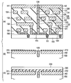
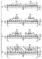
- 1 is a cross-sectional view showing an element structure of a stacked semiconductor device according to a first embodiment. It is an equivalent circuit diagram showing an example in which the stacked semiconductor device of the first embodiment is applied to a CMOS inverter. 1 is a layout diagram illustrating an example in which the stacked semiconductor device according to the first embodiment is applied to a CMOS inverter. 1 is an equivalent circuit diagram illustrating an example in which the stacked semiconductor device according to the first embodiment is applied to a NAND circuit. 1 is a layout diagram illustrating an example in which the stacked semiconductor device according to the first embodiment is applied to a NAND circuit. It is a figure which shows the threshold value characteristic of pMOSFET and GeMOSFET of Ge channel. It is sectional drawing which shows the manufacturing process of the laminated semiconductor device concerning 2nd Embodiment. It is sectional drawing which shows the manufacturing process of the laminated semiconductor device concerning 2nd Embodiment.
- FIG. 1 is a cross-sectional view showing the element structure of the stacked semiconductor device according to the first embodiment.
- a base CMOS circuit (first complementary semiconductor device) 100 is formed on the Si support substrate 110. Specifically, an nMOSFET and a pMOSFET comprising a gate insulating film 112, a gate electrode 113, and source / drain regions (not shown) are formed on the substrate 110, and multilayer wiring layers 131 to 134 are formed thereon. By forming this, a Si-CMOS circuit is manufactured. In the uppermost layer, metal electrodes 141 and 142 are formed by the same process as the wiring layers 131 to 134 and the vias 120 to 129.
- a work function control layer 211 for pMOS is formed on the metal electrode 141, and a work function control layer 212 for nMOS is formed on the metal electrode 142.
- a semiconductor layer 231 mainly composed of Ge is formed with an interlayer insulating film 220 interposed therebetween.
- a pMOSFET composed of a gate insulating film 241, a gate electrode 251, and a metal S / D 261 is formed on the semiconductor layer 231.
- a semiconductor layer 232 mainly composed of Ge is formed with an interlayer insulating film 220 interposed therebetween.
- an nMOSFET composed of a gate insulating film 242, a gate electrode 252, and a metal S / D 262 is formed. That is, an upper layer CMOS circuit (second complementary semiconductor device) using Ge as a channel is formed.
- 111 denotes an element isolation insulating film
- 114 denotes a gate sidewall insulating film
- 150 denotes an interlayer insulating film for a lower CMOS circuit.
- reference numeral 270 denotes an interlayer insulating film for the upper layer CMOS circuit
- 280 denotes a via for the upper layer CMOS circuit
- 290 denotes a wiring layer for the upper layer CMOS circuit.
- the lower layer is the Si-CMOS circuit 100
- the upper layer Ge-CMOS circuit 200 made of pMOSFET and nMOSFET using Ge as a channel is formed above the Si-CMOS circuit via the interlayer film.
- the lower-layer Si-CMOS circuit 100 and the upper-layer Ge-CMOS circuit 200 are integrated by being electrically connected via via wiring.
- a so-called “BEOL Tr” Back End Of Line Transistor
- BEOL Tr Back End Of Line Transistor
- the mounting position of BEOL Tr. Is not limited to this layer, and the intermediate layer first layer (for example, the wiring 131) is used as a base electrode, and the case where it is mounted between the first layer and the second layer is used as the bottom layer. It can be mounted on any layer beyond this.
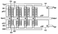
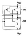
- FIGS. 2 and 3 are diagrams for explaining a CMOS circuit in which an inverter is configured by “BEOL Tr” of this embodiment
- FIG. 2 is an equivalent circuit diagram
- FIG. 3 is a layout diagram.
- metal electrodes 141 and 142 formed of a lower wiring layer are arranged. Then, Vbgp and Vbgn can be independently applied to the metal electrodes 141 and 142 by a back gate bias power source prepared independently from the signal line.
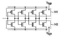
- FIGS. 4 and 5 are diagrams for explaining a CMOS circuit in which a NAND circuit is configured by “BEOL Tr.”
- FIG. 4 is an equivalent circuit diagram
- FIG. 5 is a layout diagram. Similar to the examples of FIGS. 2 and 3, metal electrodes 141 and 142 formed of lower wiring layers are arranged in each circuit block constituting the pMOSFET and nMOSFET, and Vbgp and Vbgn can be applied by a back gate bias power source. It is possible. For this reason, the threshold voltage can be controlled independently in the nMOSFET and pMOSFET in both the boost and sleep directions. Therefore, it is possible to realize a configuration capable of adaptive threshold voltage setting in accordance with the calculation frequency and required speed of the circuit.
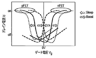
- FIG. 6 is a diagram showing threshold characteristics of a p-channel MOSFET and an n-channel MOSFET using a Ge channel.
- the solid line in FIG. 6 indicates no control, the broken line indicates a boost state by adjusting the back gate voltage (Vbgn> 0, Vbgp ⁇ 0), and the dotted line indicates a sleep state by adjusting the back gate voltage (Vbgn ⁇ 0, Vbgp ⁇ 0).
- Vbgn> 0, Vbgp ⁇ 0 the back gate voltage
- Vbgp ⁇ 0 the back gate voltage
- the on-current increases and is suitable for high-speed operation.
- the sleep state off-state current is reduced and low power consumption operation is possible.
- the threshold values of the pMOSFET and nMOSFET using the Ge channel can be shifted, and the performance of the Ge-CMOS circuit can be adjusted to the characteristics required for the device. it can.
- BEOL Tr. Formed in the wiring intermediate layer or uppermost layer has a higher mobility than a-Si in both nMOSFET and pMOSFET, and is composed of a poly-Ge channel that is expected to increase current driving capability. .
- Each transistor is formed on metal electrodes (GP) 141 and 142 formed simultaneously with the wiring layer via work function control layers 211 and 212 and an interlayer insulating film 220. Then, for each of the nMOSFET and the pMOSFET in the GP, voltage control is performed by a power source line independent from the so-called “FEOL” Tr. (Front “End” Of “Line Transistor”) and “BEOL” Tr. By performing the above, dynamic threshold control can be performed.
- BEOL Tr. May be either depletion type operation or inversion type operation for both nMOSFET and pMOSFET.
- the work function control layers 211 and 212 deposited on the GP can set threshold values according to circuit requirements.
- BEOL Tr. In the conventional structure, the performance and process cost of BEOL Tr. Formed in the wiring intermediate layer or the uppermost layer are contradictory and cannot satisfy both at the same time. In contrast, in the present embodiment, it is possible to form BEOL Tr. ⁇ ⁇ ⁇ ⁇ having an appropriate threshold value and current driving capability at a process temperature that does not degrade the underlying CMOS circuit (FEOL Tr.).
- the Ge channel As described above, according to the present embodiment, by using the Ge channel as the upper CMOS circuit 200, it is possible to lower the process temperature and improve the performance (lower voltage) by the mobility higher than that of Si. In addition, since the wiring process and the back gate (Grand plane) forming process can be merged, the cost can be reduced. Further, the metal electrodes 141 and 142 can constitute a back gate, and can be formed in common with nMOSFETs and pMOSFETs. Thus, the problem of gate depletion, which is a problem in the conventional method of forming GP by ion implantation into a semiconductor, can also be avoided.
- the threshold value can be appropriately set by the work function control layers 211 and 212 deposited on the GP, the power consumption can be reduced by reducing the off-current during standby. Furthermore, even under the above threshold setting, by biasing the back gate (GP) voltage to the boost side, adaptive power control can be realized such that the threshold setting is lowered only when high speed operation is required. This contributes to high performance, low power consumption and low cost of 3D-CMOS. Further, since the source / drain is made of NiGe alloy, there is an advantage that the resistance of the source / drain can be reduced.
- the combination of the channel material, polarity, and electrode structure of this configuration comprehensively solves the problems of the background art, thereby improving the performance, power consumption, and cost of 3D CMOS. Can contribute.
- a pMOSFET and an nMOSFET are formed on a Si support substrate 11 by a known process. These are connected by wiring layers 131 to 134 and vias 120 to 129, thereby forming a Si-CMOS circuit (first complementary semiconductor device) 100.
- the pMOS metal electrode 141 and the nMOS metal electrode 142 are formed on the uppermost layer by the same process as the wiring layers 131 to 134.
- a via 129 that is electrically connected to the transistor of the Si-CMOS circuit 100 is exposed on the uppermost surface of the Si-CMOS circuit 100.
- a so-called damascene process can be used. For example, after providing grooves corresponding to the pattern of the back gate of “BEOL” Tr. “On the surface of the interlayer insulating film 150, a metal material is deposited on the entire surface. Then, the metal electrodes 141 and 142 are formed only in the grooves by planarizing the surface by CMP.
- a barrier metal may be formed in the groove before forming the metal film.
- a barrier metal may be formed in a portion in contact with the interlayer insulating film 150. Further, for the vias 120 to 129, a barrier metal may be formed at the interface with the base as necessary.
- a pMOSFET work function control layer 211 is formed in the pMOS region by an n and p generation process using a normal lithography process, and the nMOS An nMOSFET work function control layer 212 is formed in the region.
- a TiN film (work function control layer) 211 is formed on the metal electrode 141 by sputtering, and an HfO 2 / TiN film (work function control layer) 212 is formed on the metal electrode 142 by sputtering.
- an a-Ge layer 230 having a thickness of 30 nm to be a channel of the upper CMOS circuit is formed by CVD or It is formed by sputtering.
- the active pattern is separated into islands by mesa etching in accordance with the pMOS region and the nMOS region, and then a-Ge is polycrystallized by low-temperature annealing at 500 ° C. or lower.
- Ge layers 231 and 232 are formed. That is, the polyGe layer 231 is formed on the metal electrode 141 serving as the back gate for the pMOSFET via the work function control layer 211 and the interlayer insulating film 220. Further, a poly Ge layer 232 is formed on the metal electrode 142 serving as a back gate for the nMOSFET via the work function control layer 212 and the interlayer insulating film 220.
- the metal electrodes 141 and 142 exist on the base of the a-Ge layer 230, heat easily escapes when the a-Ge layer 230 is annealed. Thereby, crystallization is promoted and the crystal grains can be increased.
- the annealed Ge layers 231 and 232 are polycrystalline. However, when the device is miniaturized and the channel length is close to the grain size, even if polycrystalline, it is regarded as substantially the same as a single crystal. Is possible.
- an Al 2 O 3 film (4 nm) formed by ALD film formation at 250 ° C. or SiO 2 (5 nm) formed by PECVD is deposited on the Ge layers 231 and 232 as a gate insulating film.
- a TaN film (30 nm) is deposited thereon by sputtering.
- a gate electrode is formed by gate patterning and etching by a normal lithography process. That is, the gate electrode 251 is formed in the pMOS region through the gate insulating film 241, and the gate electrode 252 is formed in the nMOS region through the gate insulating film 242. At this time, both sides of the gate electrodes 251 and 252 may be oxidized to form a sidewall insulating film.
- a metal S / D261 made of NiGe alloy formed by Ni deposition and low-temperature annealing ( ⁇ 350 ° C.) is formed on the source / drain of the pMOSFET.
- a NiGe alloy is similarly formed in an nMOSFET, but in an nMOSFET, an S (sulfur) impurity is implanted before Ni deposition, and a metal S / D262 having a structure in which a high concentration sulfur segregation region is formed at the NiGe / Ge interface at the time of NiGe formation is formed. To do.
- the Schottky barrier between the metal S / D layer (NiGe) 262 and the Ge layer 232 can be controlled, the parasitic resistance can be lowered, and the drive current can be increased. Thereafter, the unreacted Ni film is removed with dilute hydrochloric acid or the like.
- the contact holes for connecting to the metal electrodes 141 and 142 serving as back gates and the source / drain regions 251 and 252 respectively. Form.
- a conductive material such as Cu is embedded in the contact hole, and then planarized by CMP.
- the Al wiring layer 290 and forming the CMOS circuit the structure shown in FIG. 1 is completed. Further, a passivation film is formed as necessary.
- the wiring layer 290 may also be formed by a damascene process in the same manner as the metal electrodes 141 and 142 and the other wiring layers 131 to 134. That is, a wiring groove may be provided together with the contact hole in the step of FIG. 8G, and a metal material may be embedded in the wiring groove.
- both the pMOS and nMOS use the poly Ge layer 230 having higher mobility than a-Si as a channel, so that a higher speed device can be manufactured. Moreover, since Ge can be formed at a lower temperature than Si, the influence on the lower Si-CMOS circuit 100 when the upper Ge-CMOS circuit 200 is formed can be reduced.
- the formation substrate of the second complementary semiconductor device is not necessarily limited to the Ge layer, and any substrate having Ge as a main component may be used. Furthermore, the formation substrate of the first complementary semiconductor device is not necessarily limited to the Si substrate, and a Ge substrate can be used, and a compound semiconductor can also be used.
- the source / drain is formed of NiGe as the Ge channel MOSFET structure of the second complementary semiconductor device.
- the present invention is not limited to this, and other metals such as alloys of Co, Pd, Pt and Ge are used. Can do.
- the source / drain is not necessarily limited to an alloy, and may be a diffusion layer formed by impurity doping.
- the Ge channel MOSFET may have a so-called junctionless transistor structure having no pn junction between the source / drain (S / D) and the channel.
- chalcogen elements such as Se and Te can also be used.
- a combination of chalcogen elements S, Se, Te may be doped.
- impurities suitable for n-type and p-type with respect to the Ge channel may be dope.
- Si-CMOS circuit (first complementary semiconductor device) DESCRIPTION OF SYMBOLS 110 ... Si support substrate 111 ... Element isolation insulating film 112 ... Gate insulating film 113 ... Gate electrode 114 ... Gate side wall insulating film 120-129 ... Via 131-134 ... Wiring layer 141, 142 ... Metal electrode (back gate electrode) 150 ... interlayer insulating film 200 ... Ge-CMOS circuit (second complementary semiconductor device) 211, 212 ... work function control layer 220 ... interlayer insulating film 230 ... a-Ge layer 231, 232 ... poly Ge layer 241, 242 ... gate insulating film 251, 252 ... gate electrode 261, 262 ... metal S / D 270 ... Interlayer insulating film 280 ... Via 290 ... Wiring layer
Landscapes
- Metal-Oxide And Bipolar Metal-Oxide Semiconductor Integrated Circuits (AREA)
- Thin Film Transistor (AREA)
- Chemical & Material Sciences (AREA)
- Engineering & Computer Science (AREA)
- Composite Materials (AREA)
- Materials Engineering (AREA)
- Crystallography & Structural Chemistry (AREA)
- Recrystallisation Techniques (AREA)
- Electrodes Of Semiconductors (AREA)
- Internal Circuitry In Semiconductor Integrated Circuit Devices (AREA)
- General Engineering & Computer Science (AREA)
Abstract
La présente invention porte sur un dispositif à semi-conducteurs empilé qui comprend : un premier dispositif à semi-conducteurs complémentaire (100) dans lequel un circuit CMOS et une couche de câblage sont formés sur un substrat de semi-conducteur (110) ; des électrodes métalliques (141, 142) qui sont formées sur le premier dispositif à semi-conducteurs complémentaire (100) ensemble avec une couche de câblage ; des couches semi-conductrices (231, 232) qui sont formées sur les électrodes métalliques (141, 142) avec un film isolant (220) étant interposé entre celles-ci, qui sont formées séparément dans une zone nMOS et une zone pMOS, et qui contiennent du Ge en tant que composant principal ; et un second dispositif à semi-conducteurs complémentaire (200) dans lequel un nMOSFET est formé dans la couche semi-conductrice dans la zone nMOS et un pMOSFET est formé dans la couche semi-conductrice dans la zone pMOS.
Priority Applications (1)
| Application Number | Priority Date | Filing Date | Title |
|---|---|---|---|
| US14/577,209 US9721951B2 (en) | 2012-06-19 | 2014-12-19 | Semiconductor device using Ge channel and manufacturing method thereof |
Applications Claiming Priority (2)
| Application Number | Priority Date | Filing Date | Title |
|---|---|---|---|
| JP2012138103A JP5826716B2 (ja) | 2012-06-19 | 2012-06-19 | 半導体装置及びその製造方法 |
| JP2012-138103 | 2012-06-19 |
Related Child Applications (1)
| Application Number | Title | Priority Date | Filing Date |
|---|---|---|---|
| US14/577,209 Continuation US9721951B2 (en) | 2012-06-19 | 2014-12-19 | Semiconductor device using Ge channel and manufacturing method thereof |
Publications (1)
| Publication Number | Publication Date |
|---|---|
| WO2013190863A1 true WO2013190863A1 (fr) | 2013-12-27 |
Family
ID=49768473
Family Applications (1)
| Application Number | Title | Priority Date | Filing Date |
|---|---|---|---|
| PCT/JP2013/055527 Ceased WO2013190863A1 (fr) | 2012-06-19 | 2013-02-28 | Dispositif à semi-conducteurs empilé et procédé de fabrication associé |
Country Status (4)
| Country | Link |
|---|---|
| US (1) | US9721951B2 (fr) |
| JP (1) | JP5826716B2 (fr) |
| TW (1) | TWI525795B (fr) |
| WO (1) | WO2013190863A1 (fr) |
Cited By (1)
| Publication number | Priority date | Publication date | Assignee | Title |
|---|---|---|---|---|
| US20150214256A1 (en) * | 2014-01-30 | 2015-07-30 | Semiconductor Energy Laboratory Co., Ltd. | Semiconductor device, electronic device, and manufacturing method of semiconductor device |
Families Citing this family (14)
| Publication number | Priority date | Publication date | Assignee | Title |
|---|---|---|---|---|
| US10074576B2 (en) * | 2014-02-28 | 2018-09-11 | Semiconductor Energy Laboratory Co., Ltd. | Semiconductor memory device |
| US9330967B2 (en) | 2014-05-16 | 2016-05-03 | Taiwan Semiconductor Manufacturing Company Limited | Method of fabricating a semiconductor device with reduced leak paths |
| US9287257B2 (en) * | 2014-05-30 | 2016-03-15 | Taiwan Semiconductor Manufacturing Company, Ltd. | Power gating for three dimensional integrated circuits (3DIC) |
| KR102653044B1 (ko) * | 2015-09-01 | 2024-04-01 | 소니그룹주식회사 | 적층체 |
| FR3064396B1 (fr) * | 2017-03-27 | 2019-04-19 | Commissariat A L'energie Atomique Et Aux Energies Alternatives | Cellule memoire sram |
| US11018134B2 (en) | 2017-09-26 | 2021-05-25 | Taiwan Semiconductor Manufacturing Co., Ltd. | Semiconductor device and method for manufacturing the same |
| FR3073977B1 (fr) * | 2017-11-22 | 2021-12-03 | Commissariat Energie Atomique | Transistors de circuit 3d a grille retournee |
| FR3076076B1 (fr) * | 2017-12-22 | 2021-12-17 | Commissariat Energie Atomique | Assemblage ameliore pour circuit 3d a niveaux de transistors superposes |
| US20200058646A1 (en) * | 2018-08-14 | 2020-02-20 | Intel Corporation | Structures and methods for large integrated circuit dies |
| WO2020055642A2 (fr) * | 2018-09-05 | 2020-03-19 | Tokyo Electron Limited | Réseau de distribution d'énergie pour logique 3d et mémoire |
| EP3660924B1 (fr) * | 2018-11-30 | 2025-12-24 | IMEC vzw | Empilement de grille pmos à faible budget thermique |
| US12433019B2 (en) | 2019-11-01 | 2025-09-30 | Semiconductor Energy Laboratory Co., Ltd. | Semiconductor device |
| KR102877095B1 (ko) * | 2021-04-13 | 2025-10-28 | 삼성전자주식회사 | 반도체 소자 및 그의 제조 방법 |
| KR102767182B1 (ko) | 2021-09-24 | 2025-02-14 | 한국전자통신연구원 | 산화물 반도체를 포함하는 cmos 로직 소자 |
Citations (8)
| Publication number | Priority date | Publication date | Assignee | Title |
|---|---|---|---|---|
| JPH0590517A (ja) * | 1991-09-30 | 1993-04-09 | Toshiba Corp | 半導体装置及びその製造方法 |
| JP2006210828A (ja) * | 2005-01-31 | 2006-08-10 | Fujitsu Ltd | 半導体装置とその製造方法 |
| JP2006344941A (ja) * | 2005-06-10 | 2006-12-21 | Sharp Corp | Cmos集積回路の製造に用いるゲルマニウム・エピタキシャル膜を絶縁体上で成長させる方法 |
| JP2007251131A (ja) * | 2006-03-15 | 2007-09-27 | Sharp Corp | シリコン−ゲルマニウム立体構造cmos上の局所配線の製造方法 |
| JP2010141230A (ja) * | 2008-12-15 | 2010-06-24 | Renesas Electronics Corp | 半導体装置及び半導体装置の製造方法 |
| JP2011142314A (ja) * | 2009-12-11 | 2011-07-21 | Semiconductor Energy Lab Co Ltd | 半導体装置 |
| JP2012028731A (ja) * | 2010-06-22 | 2012-02-09 | Renesas Electronics Corp | 半導体装置、及び、半導体装置の製造方法 |
| JP2012084851A (ja) * | 2010-09-13 | 2012-04-26 | Semiconductor Energy Lab Co Ltd | 半導体装置 |
Family Cites Families (5)
| Publication number | Priority date | Publication date | Assignee | Title |
|---|---|---|---|---|
| DE69940074D1 (de) * | 1998-09-14 | 2009-01-22 | Panasonic Corp | Verfahren zur herstellung einer halbleitervorrichtung |
| US20100190334A1 (en) * | 2003-06-24 | 2010-07-29 | Sang-Yun Lee | Three-dimensional semiconductor structure and method of manufacturing the same |
| JP5007250B2 (ja) | 2008-02-14 | 2012-08-22 | ルネサスエレクトロニクス株式会社 | 半導体装置の製造方法 |
| JP2011151134A (ja) * | 2010-01-20 | 2011-08-04 | Renesas Electronics Corp | 半導体装置、および、半導体装置の製造方法 |
| FR2961016B1 (fr) * | 2010-06-07 | 2013-06-07 | Commissariat Energie Atomique | Circuit integre a dispositif de type fet sans jonction et a depletion |
-
2012
- 2012-06-19 JP JP2012138103A patent/JP5826716B2/ja not_active Expired - Fee Related
-
2013
- 2013-02-28 WO PCT/JP2013/055527 patent/WO2013190863A1/fr not_active Ceased
- 2013-03-12 TW TW102108627A patent/TWI525795B/zh not_active IP Right Cessation
-
2014
- 2014-12-19 US US14/577,209 patent/US9721951B2/en active Active
Patent Citations (8)
| Publication number | Priority date | Publication date | Assignee | Title |
|---|---|---|---|---|
| JPH0590517A (ja) * | 1991-09-30 | 1993-04-09 | Toshiba Corp | 半導体装置及びその製造方法 |
| JP2006210828A (ja) * | 2005-01-31 | 2006-08-10 | Fujitsu Ltd | 半導体装置とその製造方法 |
| JP2006344941A (ja) * | 2005-06-10 | 2006-12-21 | Sharp Corp | Cmos集積回路の製造に用いるゲルマニウム・エピタキシャル膜を絶縁体上で成長させる方法 |
| JP2007251131A (ja) * | 2006-03-15 | 2007-09-27 | Sharp Corp | シリコン−ゲルマニウム立体構造cmos上の局所配線の製造方法 |
| JP2010141230A (ja) * | 2008-12-15 | 2010-06-24 | Renesas Electronics Corp | 半導体装置及び半導体装置の製造方法 |
| JP2011142314A (ja) * | 2009-12-11 | 2011-07-21 | Semiconductor Energy Lab Co Ltd | 半導体装置 |
| JP2012028731A (ja) * | 2010-06-22 | 2012-02-09 | Renesas Electronics Corp | 半導体装置、及び、半導体装置の製造方法 |
| JP2012084851A (ja) * | 2010-09-13 | 2012-04-26 | Semiconductor Energy Lab Co Ltd | 半導体装置 |
Cited By (2)
| Publication number | Priority date | Publication date | Assignee | Title |
|---|---|---|---|---|
| US20150214256A1 (en) * | 2014-01-30 | 2015-07-30 | Semiconductor Energy Laboratory Co., Ltd. | Semiconductor device, electronic device, and manufacturing method of semiconductor device |
| TWI662653B (zh) * | 2014-01-30 | 2019-06-11 | Semiconductor Energy Laboratory Co., Ltd. | 半導體裝置、電子裝置及半導體裝置的製造方法 |
Also Published As
| Publication number | Publication date |
|---|---|
| JP2014003184A (ja) | 2014-01-09 |
| TWI525795B (zh) | 2016-03-11 |
| JP5826716B2 (ja) | 2015-12-02 |
| US20150102419A1 (en) | 2015-04-16 |
| US9721951B2 (en) | 2017-08-01 |
| TW201401487A (zh) | 2014-01-01 |
Similar Documents
| Publication | Publication Date | Title |
|---|---|---|
| JP5826716B2 (ja) | 半導体装置及びその製造方法 | |
| US11721701B2 (en) | Semiconductor circuit with metal structure and manufacturing method | |
| JP7438237B2 (ja) | 積層型縦型輸送電界効果トランジスタのためのハイブリッド・ゲート・スタック集積 | |
| US10580709B2 (en) | Flipped vertical field-effect-transistor | |
| KR102344126B1 (ko) | 후측면 전력 공급 회로를 포함한 반도체 디바이스 | |
| CN102738168B (zh) | 半导体装置及其制造方法 | |
| US11257761B2 (en) | Logic cell structure and method | |
| JP2005251873A (ja) | 半導体集積回路およびその製造方法 | |
| JP2010056215A (ja) | 縦型電界効果トランジスタを備える半導体装置及びその製造方法 | |
| JP2014127703A (ja) | 半導体装置及び半導体装置の製造方法 | |
| TW202201552A (zh) | 半導體裝置結構 | |
| WO2013161331A1 (fr) | Dispositif à semi-conducteur complémentaire et son procédé de fabrication | |
| JP6271982B2 (ja) | 半導体装置及びその製造方法 | |
| JP6273406B2 (ja) | 半導体装置及びその製造方法 | |
| JP6543392B2 (ja) | 半導体装置 | |
| JP2015103531A (ja) | 半導体装置 | |
| JP6125802B2 (ja) | 半導体装置 | |
| JP2012142493A (ja) | 半導体装置及びその製造方法 |
Legal Events
| Date | Code | Title | Description |
|---|---|---|---|
| 121 | Ep: the epo has been informed by wipo that ep was designated in this application |
Ref document number: 13807079 Country of ref document: EP Kind code of ref document: A1 |
|
| NENP | Non-entry into the national phase |
Ref country code: DE |
|
| 122 | Ep: pct application non-entry in european phase |
Ref document number: 13807079 Country of ref document: EP Kind code of ref document: A1 |