WO2013190882A1 - Transistor à oxyde métallique - Google Patents
Transistor à oxyde métallique Download PDFInfo
- Publication number
- WO2013190882A1 WO2013190882A1 PCT/JP2013/060583 JP2013060583W WO2013190882A1 WO 2013190882 A1 WO2013190882 A1 WO 2013190882A1 JP 2013060583 W JP2013060583 W JP 2013060583W WO 2013190882 A1 WO2013190882 A1 WO 2013190882A1
- Authority
- WO
- WIPO (PCT)
- Prior art keywords
- metal oxide
- drain
- gate
- characteristic
- transistor
- Prior art date
- Legal status (The legal status is an assumption and is not a legal conclusion. Google has not performed a legal analysis and makes no representation as to the accuracy of the status listed.)
- Ceased
Links
Images


Classifications
-
- H—ELECTRICITY
- H10—SEMICONDUCTOR DEVICES; ELECTRIC SOLID-STATE DEVICES NOT OTHERWISE PROVIDED FOR
- H10D—INORGANIC ELECTRIC SEMICONDUCTOR DEVICES
- H10D30/00—Field-effect transistors [FET]
- H10D30/60—Insulated-gate field-effect transistors [IGFET]
- H10D30/67—Thin-film transistors [TFT]
- H10D30/674—Thin-film transistors [TFT] characterised by the active materials
- H10D30/6755—Oxide semiconductors, e.g. zinc oxide, copper aluminium oxide or cadmium stannate
-
- H—ELECTRICITY
- H03—ELECTRONIC CIRCUITRY
- H03K—PULSE TECHNIQUE
- H03K17/00—Electronic switching or gating, i.e. not by contact-making and –breaking
- H03K17/51—Electronic switching or gating, i.e. not by contact-making and –breaking characterised by the components used
- H03K17/56—Electronic switching or gating, i.e. not by contact-making and –breaking characterised by the components used by the use, as active elements, of semiconductor devices
- H03K17/687—Electronic switching or gating, i.e. not by contact-making and –breaking characterised by the components used by the use, as active elements, of semiconductor devices the devices being field-effect transistors
-
- H—ELECTRICITY
- H10—SEMICONDUCTOR DEVICES; ELECTRIC SOLID-STATE DEVICES NOT OTHERWISE PROVIDED FOR
- H10D—INORGANIC ELECTRIC SEMICONDUCTOR DEVICES
- H10D30/00—Field-effect transistors [FET]
- H10D30/60—Insulated-gate field-effect transistors [IGFET]
- H10D30/67—Thin-film transistors [TFT]
- H10D30/6729—Thin-film transistors [TFT] characterised by the electrodes
- H10D30/673—Thin-film transistors [TFT] characterised by the electrodes characterised by the shapes, relative sizes or dispositions of the gate electrodes
- H10D30/6733—Multi-gate TFTs
- H10D30/6734—Multi-gate TFTs having gate electrodes arranged on both top and bottom sides of the channel, e.g. dual-gate TFTs
-
- H—ELECTRICITY
- H10—SEMICONDUCTOR DEVICES; ELECTRIC SOLID-STATE DEVICES NOT OTHERWISE PROVIDED FOR
- H10D—INORGANIC ELECTRIC SEMICONDUCTOR DEVICES
- H10D30/00—Field-effect transistors [FET]
- H10D30/60—Insulated-gate field-effect transistors [IGFET]
- H10D30/67—Thin-film transistors [TFT]
- H10D30/6757—Thin-film transistors [TFT] characterised by the structure of the channel, e.g. transverse or longitudinal shape or doping profile
-
- H—ELECTRICITY
- H10—SEMICONDUCTOR DEVICES; ELECTRIC SOLID-STATE DEVICES NOT OTHERWISE PROVIDED FOR
- H10D—INORGANIC ELECTRIC SEMICONDUCTOR DEVICES
- H10D62/00—Semiconductor bodies, or regions thereof, of devices having potential barriers
- H10D62/80—Semiconductor bodies, or regions thereof, of devices having potential barriers characterised by the materials
-
- H—ELECTRICITY
- H10—SEMICONDUCTOR DEVICES; ELECTRIC SOLID-STATE DEVICES NOT OTHERWISE PROVIDED FOR
- H10B—ELECTRONIC MEMORY DEVICES
- H10B20/00—Read-only memory [ROM] devices
- H10B20/20—Programmable ROM [PROM] devices comprising field-effect components
- H10B20/25—One-time programmable ROM [OTPROM] devices, e.g. using electrically-fusible links
Definitions
- the present invention relates to a metal oxide transistor having a channel region formed of a metal oxide semiconductor, and more particularly to a metal oxide transistor that can be used as a nonvolatile memory element.
- Patent Document 1 As a memory element that can be used as a ROM (read only memory), an eFUSE type element shown in Patent Document 1 below and an insulating film breakdown type element shown in Patent Document 2 are known.
- the memory element described in Patent Document 1 is a resistive element having a polysilicon / silicide / silicon nitride film laminated structure, which is the same as a wiring structure employed in a normal logic LSI process, and having two terminals of a cathode and an anode. Composed.
- the resistance element is heated by flowing a large current, and the metal wiring material atoms are migrated or melted in the direction of the electron flow to cause breakage and change the resistance value between the two terminals.
- the resistance value is changed by making a laser beam or the like incident from the outside instead of flowing a large current and breaking the wiring.
- the memory element (antifuse) described in Patent Document 2 has a MOS transistor structure, and performs writing by applying a high electric field to a gate insulating film to cause dielectric breakdown.
- the element described in Patent Document 3 includes a drain electrode and a source electrode separated on an insulating film, a physical property conversion layer formed on the insulating film between the drain electrode and the source electrode, and a physical property conversion layer. And a gate electrode formed on the high dielectric film.
- the voltage applied to the gate electrode is 0 V and the voltage between the drain electrode and the source electrode exceeds the first threshold voltage, the physical property conversion layer is reduced in resistance and becomes conductive.
- a predetermined voltage higher than 0 V is applied to the gate electrode, a channel is formed in the lower layer of the physical property conversion layer, so that the voltage between the drain electrode and the source electrode is lower than the first threshold voltage.
- it will be in a conduction state. Therefore, by setting the voltage between the drain electrode and the source electrode to a voltage between the first threshold voltage and the second threshold voltage, it can be used as a switching element that switches between conduction and non-conduction depending on the application state of the gate voltage. Is possible.
- variable resistance element described in Patent Document 4 includes a first and second electrodes, a variable resistor electrically connected to both the first and second electrodes, and a dielectric layer (corresponding to a gate insulating film). Is a three-terminal variable resistance element having a control electrode opposed to the variable resistor.
- the eFUSE type memory element described in Patent Document 1 has a structure in which the element is blown by flowing a large current, variation in resistance value of the blown element after writing is large.
- the fuse material is melted and broken by heating to a high temperature, there is a risk of scattering around the melted material, and there is a risk that the adjacent material may be altered by heating the element.
- a high-density circuit cannot be arranged around the memory element, and when a semiconductor integrated circuit is configured using the memory element, high integration is hindered, which increases the chip size.
- Patent Document 2 Since the memory element described in Patent Document 2 performs writing by breaking the insulating film, it is necessary to apply a high voltage to the gate electrode. As a result, the peripheral circuit for writing becomes large in order to increase the withstand voltage, and when a semiconductor integrated circuit is configured using the memory element, the high integration is hindered, which increases the chip size.
- the current-voltage characteristics between the drain electrode and the source electrode change depending on the application state of the gate voltage, so that the conduction and non-conduction between the drain electrode and the source electrode are switched depending on the application state of the gate voltage.
- variable resistance element described in Patent Document 4 is basically a resistance element whose resistance state changes between a low resistance state and a high resistance state, it does not function as a transistor element and cannot be used as a switching element. .
- the present invention changes the state of the resistive element with low power consumption without causing physical shape changes such as migration and melting of the resistive element due to a large current and breakdown of the insulating film due to application of a high electric field. Then, it aims at providing the transistor element which can utilize the said state change as a memory element.
- the present invention provides a semiconductor thin film made of a metal oxide semiconductor, a source electrode in contact with a partial region of the semiconductor thin film, and a gate electrode facing the semiconductor thin film through a gate insulating film.
- a metal oxide transistor comprising: In an initial state, a drain current flowing from the drain electrode to the source electrode depends on a gate voltage applied between the gate electrode and the source electrode and a drain voltage applied between the drain electrode and the source electrode.
- the dependency of the drain current on the gate voltage is smaller than the first characteristic,
- the drain current changes mainly depending on the drain voltage, and transits to a second characteristic showing an ohmic resistance characteristic regardless of the gate voltage,
- the absolute value of the unit drain current which is the drain current per unit channel width, is 1 ⁇ 10 ⁇ 14 A in the range where the absolute value of the drain voltage is at least 0.1 V or more and 10 V or less.
- the drain voltage is at least 0.1 V or more and 10 V or less even when the absolute value of the unit drain current is independent of the gate voltage and the gate voltage is within the specific voltage range.
- a metal oxide transistor characterized by having a current state of 1 ⁇ 10 ⁇ 11 A / ⁇ m or more in accordance with the drain voltage within the range.
- the semiconductor thin film, the source electrode, the drain electrode, the gate electrode, and the gate insulating film are preferably thin film transistors formed on an insulating substrate.
- the metal oxide semiconductor preferably includes In, Ga, or Zn element, and particularly preferably includes InGaZnOx.
- a partial region in the semiconductor thin film has a structure in which the current density of the drain current is locally larger than other regions.
- a region sandwiched between the drain electrode and the source electrode has a U shape.
- the gate insulating film has a stacked structure including at least a first insulating film and a second insulating film having a higher dielectric constant than the first insulating film, and the first insulating film
- the hydrogen concentration in the film is lower than that of the second insulating film and the first insulating film is provided between the semiconductor thin film and the second insulating film.
- a second gate electrode facing the semiconductor thin film via an insulating film different from the gate insulating film is provided on the opposite side of the gate electrode with the semiconductor thin film interposed therebetween. It is preferable.
- the characteristic change from the first characteristic to the second characteristic is caused by Joule heat generated by the drain current, and the element constituting the metal oxide semiconductor of the semiconductor thin film is changed. It is generated by changing the composition ratio.
- the present invention provides a semiconductor device comprising the metal oxide transistor having the above characteristics.
- the present invention is a method for driving a metal oxide transistor having the above characteristics, wherein the predetermined current is applied between the drain electrode and the source electrode in a state where the metal oxide transistor exhibits the first characteristic.
- a method for driving a metal oxide transistor wherein the drain current having a density equal to or higher than the density is supplied for the predetermined time to change the characteristic of the metal oxide transistor from the first characteristic to the second characteristic.
- the metal oxide transistor having the above characteristics can be used as a transistor element in which the drain current varies depending on the gate voltage and the drain voltage under the first characteristic in the initial state.
- the absolute value of the unit drain current which is a current, is a minute current state of 1 ⁇ 10 ⁇ 14 A / ⁇ m or less, that is, a substantially non-conductive state, in the range where the absolute value of the drain voltage is at least 0.1 V to 10 V.
- Switching that switches between conduction and non-conduction between the drain electrode and the source electrode by transitioning the gate voltage between the specific voltage range and other voltage ranges because there is a specific voltage range that is the voltage range of the gate voltage Can be used as an element.
- the metal oxide transistor having the above characteristics transitions to a second characteristic that exhibits an ohmic resistance characteristic without depending on the gate voltage by allowing a drain current of a predetermined current density or more to flow through the semiconductor thin film for a predetermined time. Since the function as a transistor element and a switching element disappears and it behaves as a resistance element, it can be used as a resistance element. Further, when the gate voltage is set within the above specific voltage range, it becomes a substantially non-conductive state under the first characteristic and becomes a conductive state under the second characteristic, so that it behaves as a resistance element. Whether the first characteristic or the second characteristic is present can be determined by conduction / non-conduction, and can be used as a nonvolatile memory element.
- metal oxide transistors having the above characteristics, some of the metal oxide transistors are fixedly used as transistor elements or switching elements, and some of the other metal oxide transistors are used as the first.
- the metal oxide transistors By programming to one of the characteristic state and the second characteristic state, it can be used as a memory element that stores information in a nonvolatile manner. That is, a memory element and its peripheral circuit can be formed using the metal oxide transistor having the same characteristics as described above.
- a programmable logic device can be configured by incorporating some other metal oxide transistor memory elements into a logic circuit.
- some other metal oxide transistors can be used not only as memory elements but also as resistance elements.
- a composite device having various functions can be configured by combining transistor elements, switching elements, memory elements, and resistance elements.
- the metal oxide transistor having the above characteristics is a thin film transistor, it can be formed on the insulating substrate on which the liquid crystal display device or the like is formed in the peripheral portion of the display device, and the configuration of the peripheral circuit of the display device It can be used as an element. Further, a circuit formed of a metal oxide transistor of a thin film transistor can be stacked over an integrated circuit including bulk transistors, and thus a high-density and high-function integrated circuit can be provided.
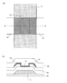
- the top view and sectional view which show typically an example of the element structure of the metal oxide transistor concerning a 1st embodiment of the present invention.
- Process sectional drawing which shows typically the element cross section in the middle of the manufacturing process of the metal oxide transistor which concerns on 1st Embodiment of this invention.
- 4A and 4B illustrate channel length and channel width of a metal oxide transistor of the present invention.
- the top view and sectional drawing which show typically another example of the element structure of the metal oxide transistor which concerns on 1st Embodiment of this invention.
- FIG. 5 is a diagram showing superimposed characteristics near the origin of the Ids-Vds characteristics shown in FIGS.
- FIG. 5 is a diagram showing the Ids-Vgs characteristics shown in FIGS.
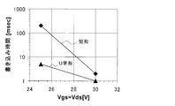
- movement of the metal oxide transistor of this invention The figure which shows an example of the relationship between the writing time, the gate voltage Vgs, and the drain voltage Vds in two types of element structures with the shape of the gap
- the top view and sectional drawing which show typically another example of the element structure of the metal oxide transistor which concerns on 1st Embodiment of this invention.
- the block diagram which shows schematic structure at the time of applying the metal oxide transistor of this invention to a display apparatus The top view and sectional view which show typically an example of the element structure of the metal oxide transistor concerning a 2nd embodiment of the present invention.
- Process sectional drawing which shows typically the element cross section in the middle of the manufacturing process of the metal oxide transistor which concerns on 2nd Embodiment of this invention.
- the top view and sectional drawing which show typically an example of the element structure of the metal oxide transistor which concerns on 3rd Embodiment of this invention.
- Process sectional drawing which shows typically the element cross section in the middle of the manufacturing process of the metal oxide transistor which concerns on 3rd Embodiment of this invention.
- the top view and sectional drawing which show typically an example of the element structure of the metal oxide transistor concerning another embodiment of this invention
- the present transistor As appropriate, an embodiment of a metal oxide transistor of the present invention (hereinafter referred to as “the present transistor” as appropriate) will be described with reference to the drawings.
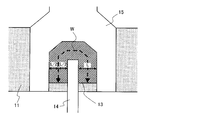
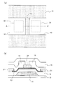
- FIG. 1 shows an example of the element structure of the transistor 1 in the first embodiment.
- FIG. 1A schematically shows a planar structure of the transistor 1
- FIG. 1B schematically shows a cross-sectional structure of the transistor 1.
- the cross section shown in FIG. 1B is a cross section taken along the line AA ′ shown in FIG.
- the transistor 1 includes an insulating substrate 10 such as a glass substrate, a gate electrode 11, a first insulating film (gate insulating film) 12 covering the gate electrode 11, a semiconductor thin film 13 made of a metal oxide semiconductor, and a source electrode. 14 and the drain electrode 15 are formed, and a second insulating film 16 is further formed thereon.
- the transistor 1 has a transistor structure similar to a bottom gate thin film transistor (TFT) manufactured over an insulator substrate.
- TFT bottom gate thin film transistor
- FIG. 2 is a cross section taken along the line A-A 'shown in FIG. 1A.
- a first conductive film is formed on the entire surface of the insulator substrate 10 by, for example, a sputtering method, and patterned by a well-known dry etching method to form a gate electrode 11.
- the first conductive film is composed of a single layer film or a laminated film of two or more layers, and includes aluminum (Al), chromium (Cr), copper (Cu), tantalum (Ta), titanium (Ti), and molybdenum (Mo).
- it is formed of a conductor made of an element selected from tungsten (W), or an alloy containing two or more of these elements as components.
- a three-layer film of Ti / Al / Ti, a three-layer film of Mo / Al / Mo, or the like can be used.
- a three-layer film of Ti having a thickness of 10 to 100 nm, Al having a thickness of 50 to 500 nm, and Ti having a thickness of 50 to 300 nm is used from the lower layer side.
- a gate insulating film 12 is formed on the entire surface of the exposed insulating substrate 10 and the gate electrode 11 by, for example, a plasma CVD method or a sputtering method.
- the gate insulating film 12 include a silicon oxide film (SiO 2 ), a silicon nitride film (SiN), a silicon oxynitride film (SiNO), a silicon nitride oxide film (SiON), aluminum oxide (Al 2 O 3 ), and tantalum oxide. It is composed of a single layer selected from (Ta 2 O 5 ) or a laminated film of two or more layers. In this embodiment, as an example, a two-layer film of SiN having a thickness of 100 to 500 nm and SiO 2 having a thickness of 20 to 100 nm is used from the lower layer side.
- a metal oxide semiconductor layer having a thickness of 20 to 200 nm is formed on the entire surface of the gate insulating film 12 by, for example, a sputtering method and patterned by a well-known wet etching method.
- a semiconductor thin film 13 is formed.
- the semiconductor thin film 13 is formed on a partial region of the gate electrode 11 via the gate insulating film 12.
- an oxide semiconductor including In, Ga, or Zn element more preferably, IGZO (InGaZnOx) which is a kind of amorphous oxide semiconductor is used. use.
- IGZO is an n-type metal oxide semiconductor containing indium (In), gallium (Ga), zinc (Zn), and oxygen (O) as main components, and has a feature that it can be formed at a low temperature.
- IGZO may also be called IZGO or GIZO.
- metal oxide semiconductor used for the semiconductor thin film 13 in addition to IGZO, NiO, SnO 2 , TiO 2 , VO 2 , In 2 O 3 , as long as the characteristic change from the first characteristic to the second characteristic described later occurs.
- An oxide semiconductor such as SrTiO 3 or an oxide semiconductor to which various impurities are added may be used.
- a second conductive film is formed on the entire surface of the exposed gate insulating film 12 and semiconductor thin film 13 by, for example, a sputtering method and patterned by a well-known dry etching method.
- a source electrode 14 and a drain electrode 15 are formed.
- the source electrode 14 and the drain electrode 15 are separated from each other and are in contact with a part of the semiconductor thin film 13.
- the region between the source electrode 14 and the drain electrode 15 has a U-shape in plan view.
- the second conductive film is composed of a single layer film or a laminated film of two or more layers, and includes aluminum (Al), chromium (Cr), copper (Cu), tantalum (Ta), titanium (Ti), and molybdenum (Mo). Alternatively, it is formed of a conductor made of an element selected from tungsten (W), or an alloy containing two or more of these elements as components.
- a three-layer film of Ti / Al / Ti, a three-layer film of Mo / Al / Mo, or the like can be used.
- a three-layer film of Ti having a thickness of 10 to 100 nm, Al having a thickness of 50 to 400 nm, and Ti having a thickness of 50 to 300 nm is used from the lower layer side.
- a second insulating film 16 is formed on the entire surface of the exposed gate insulating film 12, semiconductor thin film 13, source electrode 14 and drain electrode 15 by, for example, plasma CVD or sputtering. Film. Subsequently, annealing is performed in an air atmosphere at 200 to 400 ° C. for about 30 minutes to 4 hours.
- the second insulating film 16 includes, for example, a silicon oxide film (SiO 2 ), a silicon nitride film (SiN), a silicon oxynitride film (SiNO), a silicon nitride oxide film (SiON), aluminum oxide (Al 2 O 3 ), oxide It is composed of a single layer selected from tantalum (Ta 2 O 5 ) or a laminated film of two or more layers. In this embodiment, as an example, a single-layer film of SiO 2 having a thickness of 50 to 500 nm is used.
- a third insulating film 17 such as a photosensitive resin is formed as a planarizing film for planarizing the surface of the second insulating film 16, as shown in FIG. Perform exposure, development, and baking. Further, the formed third insulating film 17 and second insulating film 16 are etched so that the gate electrode 11, the source electrode 14, the drain electrode 15, and the like are formed on a metal wiring layer (for example, the third insulating film). , ITO, etc.) to form contact holes (not shown). Note that only the third insulating film 17 may be formed without forming the second insulating film 16.
- the channel length L and the channel width W of the transistor 1 are defined by the length and width of the gap portion on the semiconductor thin film 13 sandwiched between the source electrode 14 and the drain electrode 15, and the channel length L is the source This corresponds to the distance between the electrode 14 and the drain electrode 15 on the semiconductor thin film 13.
- the channel width W is the length of a line segment connecting the bisectors of the separation distance of the source electrode 14 and the drain electrode 15 on the semiconductor thin film 13.
- the transistor 1 has a channel width of the transistor because the gap portion on the semiconductor thin film 13 sandwiched between the source electrode 14 and the drain electrode 15 has a U-shape in plan view.
- W is a length along a U-shaped line (shown by a broken line) that connects the source electrode 14 and the drain electrode 15 with an intermediate point that is equidistant.
- the gap portion on the semiconductor thin film 13 sandwiched between the source electrode 14 and the drain electrode 15 does not have to be U-shaped in plan view.
- a rectangular shape may be used as shown in FIG.
- the transistor 1 is an n-channel transistor when the above-described IGZO is used as the metal oxide semiconductor of the semiconductor thin film 13.
- the drain current Ids current flowing from the drain electrode to the source electrode
- the gate voltage Vgs voltage applied to the gate electrode with respect to the source electrode
- the drain voltage Vds as in a normal thin film transistor.
- the voltage varies depending on each of (the voltage applied to the drain electrode with reference to the source electrode).
- the gate length L of the transistor 1 used for measuring the characteristics shown in FIG. 5 is 4 ⁇ m, the gate width W is 20 ⁇ m, and the shape of the gap is rectangular or U-shaped.
- the drain current Ids of each characteristic indicates the value of the unit drain current with the unit gate width (1 ⁇ m).
- the transistor 1 in the initial state exhibits the same characteristics (corresponding to the first characteristics) as a normal thin film transistor, and the gate voltage Vgs is about 0.5 V or less.
- the unit drain current is in a very small current state of 1 ⁇ 10 ⁇ 14 A / ⁇ m or less when the drain voltage is at least 0.1 V or more and 10 V or less, It is substantially in the off state.
- the drain current Ids increases with an increase in the gate voltage Vgs and increases with an increase in the drain voltage Vds.
- the transistor 1 In the initial state showing the transistor characteristics (first characteristics), the transistor 1 applies a higher voltage than the voltage application range in the circuit operation used as a normal transistor element to the gate voltage Vgs and causes a large drain current to flow. By generating Joule heat locally in the semiconductor thin film 13 through which the drain current flows, the electrical characteristics change from the initial transistor characteristics to ohmic resistance characteristics (corresponding to the second characteristics). There is.
- the operation for changing the electrical characteristics from the transistor characteristics to the ohmic resistance characteristics is referred to as a write operation for convenience.
- the drain current Ids of each characteristic indicates the value of the unit drain current with the unit gate width (1 ⁇ m).
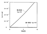
- FIG. 8 shows the Ids-Vgs characteristic under the first characteristic in FIG. 5A and the Ids-Vgs characteristic under the second characteristic in FIG.
- FIG. 9 shows differential resistance (dVds / dIds, unit: ⁇ m) obtained from the Ids-Vds characteristic under the first characteristic in FIG. 5B and the Ids-Vds characteristic under the second characteristic in FIG. 6B.
- the relationship between the differential resistance (dVds / dIds, unit: ⁇ m) obtained from the above and the drain voltage Vds is shown for gate voltages Vgs of 0V and 7V.
- the drain current Ids varies greatly depending on the gate voltage Vgs under the first characteristics in the initial state, and the gate voltage Vgs is within the specific voltage range ( When it is approximately 0.5 V or less), the drain current Ids is substantially in an off state with little flow, but when transitioning to the second characteristic, the drain current Ids is within a specific voltage range regardless of the gate voltage Vgs.
- the unit drain current is 1 ⁇ 10 ⁇ 11 A / ⁇ m or more.
- the differential resistance under the first characteristic varies depending on the gate voltage Vgs regardless of the drain voltage Vds, but the differential resistance under the second characteristic is independent of the drain voltage Vds. It does not change with the gate voltage Vgs.
- the writing operation of the transistor 1 is such that the drain current Ids having a high current density is applied to the semiconductor thin film 13 at a constant level in a bias state higher than the voltage range of the gate voltage Vgs and the drain voltage Vds applied to the transistor 1 under the first characteristic. It is executed by flowing the writing time.
- the drain current Ids having a high current density flows in the semiconductor thin film 13 for a certain writing time, Joule heat and electromigration occur in the semiconductor thin film 13 due to the drain current Ids, and the metal oxide semiconductor constituting the semiconductor thin film 13 It is considered that the above-described characteristic change is induced by changing the composition.
- the unit drain current (unit: A / ⁇ m) is proportional to the current density (unit: A / m 2 ) of the drain current.
- Increasing the unit drain current (unit: A / ⁇ m) increases the current density (unit: A / m 2 ) of the drain current.
- the unit drain current and the write time during the write operation are assumed to be about 1 ⁇ A / ⁇ m to 1 mA / ⁇ m and about 10 ⁇ sec to 100 seconds. Note that the unit drain current and the writing time during the writing operation vary depending on the metal oxide semiconductor used for the semiconductor thin film 13 and the element structure of the transistor 1, and thus are limited to the above numerical range. is not.
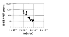
- FIG. 10 shows an example of the relationship between the write time (unit: msec) and the unit drain current (unit: A / ⁇ m).
- FIG. 10 shows that the larger the unit drain current, the shorter the writing time.
- the writing characteristics change depending on the element structure of the transistor 1. For example, in an element structure in which Joule heat is likely to be generated or an element structure in which Joule heat is not easily diffused, the writing characteristics are low. improves.
- Vgs Vds
- Vgs Vds
- two types of transistors 1 having different element structures are connected in series and each has a first characteristic.
- the write operation is completed in the transistor 1 with a higher current density and the transition is made to the second characteristic, so that the write operation is not completed in the transistor 1 with a lower current density. Since the first characteristic is maintained, the drain current is cut off when one of the write operations is completed, so that only one of the transistors 1 can be shifted to the second characteristic.
- the gate insulating film 12 When the high gate voltage Vgs is applied for the write operation to increase the drain current Ids, the gate insulating film 12 may be broken down. For this reason, in this embodiment, in order to maintain the gate voltage Vgs lower than the breakdown voltage of the gate insulating film 12 and increase the drain current Ids, the gate insulating film 12 is made of a material having a high relative dielectric constant. The capacity is increased. In the above example, the relative dielectric constant of the silicon nitride film (SiN) and the silicon oxynitride film (SiNO) is higher than that of the silicon oxide film (SiO 2 ).
- the silicon oxide film (SiO 2 ) or the silicon nitride oxide film (SiON) contains hydrogen in the film formed by the CVD method, and the hydrogen reacts with oxygen of the metal oxide semiconductor of the semiconductor thin film 13. Since the semiconductor thin film 13 approaches the conductor from the semiconductor, the semiconductor thin film 13 and the relative dielectric constant are prevented from coming into direct contact with the silicon nitride film (SiN) or silicon oxynitride film (SiNO) having a high relative dielectric constant.
- a silicon oxide film (SiO 2 ) or a silicon nitride oxide film (SiON) having a low hydrogen concentration in the film is preferably inserted between the silicon nitride film (SiN) or the silicon oxynitride film (SiNO) having a high thickness.
- the semiconductor thin film 13 is covered with the second insulating film 16 and the third insulating film 17, and at least a part thereof is covered. It is also preferable that a second gate electrode 18 made of a conductor is provided so that is located above the gate electrode 11, and the second gate electrode 18 and the gate electrode 11 are connected via a contact hole 19. As a result, the second gate electrode 18 and the gate electrode 11 have the same potential, the drain current Ids increases due to the back gate effect, and the transition from the first characteristic to the second characteristic is likely to occur.
- Fig.12 (a) the top view which saw through the 2nd gate electrode 18 is shown.
- the transistor 1 the electrical characteristics change dramatically from the first characteristics to the second characteristics by the above-described write operation, and in particular, when the gate voltage Vgs is within a specific voltage range (about 0.5 V or less). Therefore, the transistor 1 can be used as a nonvolatile memory element by using the current difference. That is, one of binary information “0” and “1” is assigned to the first characteristic before the write operation, and the other of binary information “0” and “1” is assigned to the second characteristic after the write operation. By assigning a predetermined voltage (for example, 0 V) within a specific voltage range to the gate voltage Vgs and detecting the magnitude of the drain current Ids, the transistor 1 has either the first characteristic or the second characteristic. It is possible to determine whether it is in a state.
- a predetermined voltage for example, 0 V
- the transistor 1 under the first characteristic before the write operation (initial state), the transistor 1 is used as a switching element because the drain current Ids hardly flows when the gate voltage Vgs is within a specific voltage range. Can do. Further, in the transistor 1, under the first characteristic before the write operation (initial state), when the gate voltage Vgs is higher than the specific voltage range, the drain current Ids changes depending on the gate voltage Vgs and the drain voltage Vds, respectively. Therefore, it can be used as an amplifying element. Furthermore, since the transistor 1 exhibits ohmic resistance characteristics under the second characteristics after the writing operation, it can be used as a resistance element.
- the capacitor element is formed by etching and removing the metal oxide semiconductor layer on a part of the gate electrode 11 in the manufacturing process shown in FIG.
- the thin film 13 is not formed, and the second conductive film is left on the gate electrode 11 without being removed by etching in the manufacturing process shown in FIG.
- a capacitive element is formed with a gate insulating film 12 sandwiched between 11 and the remaining second conductive film.
- the transistor 1 can be used as a switching element, an amplifying element, and a resistance element in addition to a memory element, and a capacitor element is formed in the same manufacturing process. Therefore, various semiconductor devices using the transistor 1 can be manufactured. Can be configured. For example, a semiconductor memory device including a memory circuit using the transistor 1 as a memory element can be configured, and a semiconductor device including a digital logic circuit using the transistor 1 as a switching element can be configured. Alternatively, a semiconductor device including an analog circuit used as a resistance element can be configured, and a semiconductor device combining these circuits can be configured. The transistor 1 may be combined with another transistor element having a different element structure to constitute a semiconductor device.
- the transistor 1 is formed as a thin film transistor, when applied to a display device such as a liquid crystal display device formed on an insulator substrate, the above-described various semiconductor devices are formed on the same insulator substrate as the display device. can do.
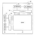
- FIG. 13 shows a schematic block configuration when the transistor 1 is applied to the display device 20.
- the display device 20 includes a display unit 21 including a plurality of pixels arranged in a matrix, a source driver 22 that drives a source line of each pixel, and a first control circuit that controls the timing and source line voltage of the source driver 22. 23, the first storage device 24 for storing the redundant repair information of the source driver 22 and the configuration parameters necessary for driving the source line, the gate driver 25 for driving the gate line of each pixel, and the timing and gate of the gate driver 25 A second control circuit 26 for controlling the line voltage and a second storage device 27 for storing redundant relief information of the gate driver 25 and configuration parameters necessary for driving the gate line are configured.
- the first and second control circuits 23 and 26 are connection terminals (not shown) constituting the contact type interface.
- the first and second control circuits 23 and 26 are wireless devices constituting the non-contact interface. Connect to a circuit (not shown).
- the transistor 1 is used as a memory element, it is incorporated in the first and second storage devices 24 and 27, and the configuration information of the display device 20, ID information, redundant relief information of each driver, and driving of source lines or gate lines It is used to store configuration parameters necessary for
- the transistor 1 when used as a memory element, it can be stored in an ID such as an IC tag because the transistor 1 can be manufactured at a relatively low temperature. Further, since the transistor 1 can be manufactured from a transparent material, the transistor 1 can be used for a mass storage device for digital signage. In addition to the memory device, by using the transistor 1 as a programming element of a logic circuit, a programmable logic circuit device such as an ASIC (Application Specific Integrated Circuit) or an FPGA (Field-Programmable Gate Array) can be realized. .
- ASIC Application Specific Integrated Circuit
- FPGA Field-Programmable Gate Array
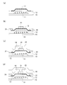
- FIG. 14 shows an example of the element structure of the transistor 2 in the second embodiment.
- FIG. 14A schematically shows a planar structure of the transistor 2
- FIG. 14B schematically shows a cross-sectional structure of the transistor 2.
- the cross section shown in FIG. 14B is a cross section taken along the line AA ′ shown in FIG.
- the gap portion on the semiconductor thin film 13 sandwiched between the source electrode 14 and the drain electrode 15 is illustrated as a rectangular shape in plan view. It may be U-shaped as shown in the plan view of FIG.
- the opening 32 of the etching stopper layer 31 positioned below the source electrode 14 and the drain electrode 15 is indicated by a dotted line, and the semiconductor thin film 13 positioned below the etching stopper layer 31 is shown.
- the side walls are indicated by broken lines.
- the transistor 2 of the second embodiment has the same basic element structure as the transistor 1 of the first embodiment.
- a characteristic difference is that in the transistor 2 of the second embodiment, an etching stopper layer 31 is formed on a partial region of the semiconductor thin film 13, and an opening 32 of the etching stopper layer 31 is formed. This is in contact with the source electrode 14 and the drain electrode 15.
- the second difference is that the semiconductor thin film 13 is formed so as to protrude from the gate electrode 11 in the gate length L direction.
- the etching stopper layer 31 is the second insulating film counted from the gate insulating film 12.
- the etching stopper layer 31 is not called the second insulating film, but the first insulating film of the first embodiment.
- the same insulating film as the second insulating film 16 (the third insulating film in the second embodiment) is used as the second insulating film 16.
- FIG. 15 is a cross section taken along the line A-A ′ shown in FIG. 14A. Moreover, the description which overlaps with 1st Embodiment is omitted.
- a first conductive film is formed on the entire surface of the insulator substrate 10 and patterned by a well-known dry etching method to form a gate electrode 11, followed by an exposed insulator.
- a gate insulating film 12 is formed on the entire surface of the substrate 10 and the gate electrode 11, and then a metal oxide semiconductor layer is formed on the entire surface of the gate insulating film 12, and patterned by a well-known wet etching method to form a semiconductor thin film. 13 is formed.
- the film forming method, material, structure, film thickness, and the like of the first conductive film, the gate insulating film 12 and the semiconductor thin film 13 are the same as those in the first embodiment.
- an etching stopper layer 31 is formed on the entire surface of the exposed gate insulating film 12 and semiconductor thin film 13 by, for example, a plasma CVD method or a sputtering method, and a known dry etching method. Pattern. Subsequently, annealing is performed in an air atmosphere at 200 to 450 ° C. for about 30 minutes to 4 hours.
- the etching stopper layer 31 includes, for example, a silicon oxide film (SiO 2 ), a silicon nitride film (SiN), a silicon oxynitride film (SiNO), a silicon nitride oxide film (SiON), aluminum oxide (Al 2 O 3 ), and tantalum oxide. It is composed of a single layer selected from (Ta 2 O 5 ) or a laminated film of two or more layers. In the present embodiment, as an example, a two-layer film of SiO 2 having a thickness of 10 to 500 nm is used.
- the etching stopper layer 31 covers the exposed surface of the gate insulating film 12, and the second conductive film used when forming the source electrode 14 and the drain electrode 15 by etching the second conductive film in a later process. It is formed on the semiconductor thin film 13 as a base layer for the portion to be removed.
- a second conductive film is formed on the entire surface of the exposed semiconductor thin film 13 and etching stopper layer 31, and is patterned by a well-known dry etching method to form the source electrode 14 and the drain.
- the electrodes 15 are formed respectively.
- the source electrode 14 and the drain electrode 15 are separated from each other and come into contact with a partial region of the semiconductor thin film 13 through the opening of the etching stopper layer 31.
- the gap between the regions where the source electrode 14 and the drain electrode 15 are in contact with the semiconductor thin film 13 has a rectangular shape in plan view. ing.
- the film forming method, material, structure, film thickness, and the like of the second conductive film are the same as in the first embodiment.
- the second insulating film 16 is formed on the entire surface of the exposed etching stopper layer 31, the semiconductor thin film 13, the source electrode 14, and the drain electrode 15. Subsequently, annealing is performed in an air atmosphere at 200 to 400 ° C. for about 30 minutes to 4 hours.
- the film forming method, material, structure, film thickness, and the like of the second insulating film 16 are the same as those in the first embodiment.
- a third insulating film such as a photosensitive resin is formed as a flattening film for flattening the surface of the second insulating film 16 as in the first embodiment. Exposure, development and baking. Furthermore, the formed third insulating film and the second insulating film 16 are etched, and the gate electrode 11, the source electrode 14, the drain electrode 15, and the like are formed on a metal wiring layer (for example, A contact hole (not shown) for connection with ITO or the like is formed. Note that only the third insulating film may be formed without forming the second insulating film 16.
- the etching stopper layer 31 is provided, damage to the semiconductor thin film 13 during the etching of the second conductive film is avoided, so that the electrical characteristics of the transistor 2 vary.
- the amount of variation in electrical characteristics due to electrical stress is reduced as compared with the transistor of the first embodiment.
- the contact between the first and second conductive films can be directly formed, the circuit area can be reduced by reducing the size of the contact hole.
- the etching stopper layer 31 is removed by etching on a part of the gate electrode 11 in the manufacturing process shown in FIG.
- the etching stopper layer 31 is not formed, and the second conductive film is left on the gate electrode 11 without being removed by etching in the manufacturing process shown in FIG.
- a capacitor element is formed in which the gate insulating film 12 and the etching stopper layer 31 are sandwiched between the gate electrode 11 and the remaining second conductive film.
- the electrical characteristics, write operation, and application example of the transistor 2 of the second embodiment are basically the same as those described in the first embodiment, and duplicate descriptions are omitted.
- FIG. 16 shows an example of the element structure of the transistor 3 in the third embodiment.
- FIG. 16A schematically shows a planar structure of the transistor 3, and
- FIG. 16B schematically shows a cross-sectional structure of the transistor 3.
- the cross section shown in FIG. 16B is a cross section along the line AA ′ shown in FIG.
- the gap portion on the semiconductor thin film 13 sandwiched between the source electrode 14 and the drain electrode 15 is illustrated as a rectangular shape in plan view. It may be U-shaped as shown in the plan view of FIG.
- the transistor 3 of the third embodiment has the same basic element structure as the transistor 1 of the first embodiment.
- a characteristic difference is that in the transistor 3 of the third embodiment, the source electrode 14 and the drain electrode 15 are in contact with the lower surface side of the semiconductor thin film 13. Therefore, unlike the first embodiment, the source electrode 14 and the drain electrode 15 are formed before the semiconductor thin film 13.
- FIG. 17 is a cross section taken along line A-A ′ shown in FIG. 16A. Moreover, the description which overlaps with 1st Embodiment is omitted.
- a first conductive film is formed on the entire surface of the insulator substrate 10 and patterned by a well-known dry etching method to form the gate electrode 11, followed by the exposed insulator.
- a gate insulating film 12 is formed on the entire surface of the substrate 10 and the gate electrode 11, and then a second conductive film is formed on the entire surface of the gate insulating film 12, and is separated from each other by patterning using a known dry etching method.
- the source electrode 14 and the drain electrode 15 are formed.
- the gap between the source electrode 14 and the drain electrode 15 has a rectangular shape in plan view.
- the film forming method, material, structure, film thickness, and the like of the first conductive film, the gate insulating film 12, and the second conductive film are the same as those in the first embodiment.
- a metal oxide semiconductor layer is formed on the entire surface of the exposed gate insulating film 12, the source electrode 14, and the drain electrode 15, and is patterned by a well-known wet etching method.
- a thin film 13 is formed.
- the semiconductor thin film 13 is in contact with the source electrode 14 and the drain electrode 15, respectively.
- the film forming method, material, structure, film thickness, etc. of the metal oxide semiconductor layer are the same as in the first embodiment.
- a second insulating film 16 is formed on the entire surface of the exposed second conductive film (source electrode 14 and drain electrode 15) and the semiconductor thin film 13. Subsequently, annealing is performed in an air atmosphere at 200 to 400 ° C. for about 30 minutes to 4 hours.
- the film forming method, material, structure, film thickness, and the like of the second insulating film 16 are the same as those in the first embodiment.
- the transistor 3 is manufactured through the above steps.
- a third insulating film (not shown) such as a photosensitive resin is formed as a flattening film for flattening the surface of the second insulating film 16 as in the first embodiment. Exposure, development and baking. Furthermore, the formed third insulating film and the second insulating film 16 are etched, and the gate electrode 11, the source electrode 14, the drain electrode 15, and the like are formed on a metal wiring layer (for example, A contact hole (not shown) for connection with ITO or the like is formed. Note that only the third insulating film may be formed without forming the second insulating film 16.
- the source electrode 14 and the drain electrode 15 are formed before the semiconductor thin film 13 in the transistor 3 of the third embodiment, no etching damage occurs in the semiconductor thin film 13 when the second conductive film is etched. Variations in the electrical characteristics of the transistor 3 and variations in the electrical characteristics due to electrical stress are reduced compared to the transistor of the first embodiment. Furthermore, compared with the second embodiment, since it is not necessary to form the etching stopper layer 31, the manufacturing process is simplified, which is advantageous in manufacturing cost and yield.
- the second conductive film is removed by etching on a part of the gate electrode 11 in the manufacturing process shown in FIG.
- the capacitor element is formed by sandwiching the gate insulating film 12 between the part of the gate electrode 11 and the remaining second conductive film.
- the electrical characteristics, write operation, and application example of the transistor 3 of the third embodiment are basically the same as those described in the first embodiment, and redundant descriptions are omitted.
- FIG. 18 shows an example of the element structure of the transistor 4 composed of a top gate type thin film transistor.
- FIG. 18A schematically shows a planar structure of the transistor 4 and
- FIG. 18B schematically shows a cross-sectional structure of the transistor 4.
- the cross section shown in FIG. 18B is a cross section taken along the line A-A ′ shown in FIG.
- a semiconductor thin film 13 made of a metal oxide semiconductor, a gate insulating film 12, and a gate electrode 11 are formed in the order of description on an insulator substrate 10 such as a glass substrate, and an interlayer is formed thereon.
- An insulating film 41 is formed, and the source electrode 14 and the drain electrode 15 formed on the interlayer insulating film 41 are connected to the semiconductor thin film 13 through the contact hole 42.
- the transistors 1 to 4 of the above embodiments and the other embodiments are constituted by thin film transistors
- the semiconductor thin film 13 made of a metal oxide semiconductor is formed on a silicon substrate instead of the insulator substrate 10. Even if the transistor structure is a MOS transistor structure, a metal oxide having an electrical characteristic that transitions from the first characteristic to the second characteristic by passing a drain current having a high current density through the semiconductor thin film 13. A transistor can be realized.
- the n-channel type transistor using IGZO which is an n-type metal oxide semiconductor, as the metal oxide semiconductor of the semiconductor thin film 13 has been described as an example.
- the type is not limited to the n-channel type.
- the materials, structures, and thicknesses of the conductive films and the insulating films constituting the transistors described in the above embodiments are examples, and the electrical characteristics and writing characteristics of the transistors are examples.
- the present invention is not limited to the contents described in each embodiment.
- the present invention can be used for a metal oxide transistor having a channel region formed of a metal oxide semiconductor, and a semiconductor device and an electronic device including the transistor.
- Metal oxide transistor 10 Insulator substrate 11: Gate electrode 12: First insulating film (gate insulating film) 13: Semiconductor thin film (metal oxide semiconductor) 14: Source electrode 15: Drain electrode 16: Second insulating film 17: Third insulating film 18: Second gate electrode 19: Contact hole 20: Display device 21: Display unit 22: Source driver 23: First control circuit 24: First memory device 25: Gate driver 26: Second control circuit 27: Second memory device 31: Etching stopper layer 32: Opening portion of etching stopper layer 41: Interlayer insulating film 42: Contact hole
Landscapes
- Thin Film Transistor (AREA)
Abstract
L'invention concerne un élément de transistor, l'état de celui-ci étant changé en celui d'un élément résistant ayant une faible consommation d'énergie sans migration et fusion de l'élément résistif dues à un grand courant, ni changements de forme physique, tels qu'une rupture d'un film isolant due à l'application d'un champ électrique élevé, et le changement d'état pouvant être utilisé en tant qu'élément mémoire. Ce transistor à oxyde métallique comprend : une couche mince de semi-conducteur (13) formée d'un semi-conducteur à oxyde métallique ; une électrode de source (14) et une électrode de drain (15), qui sont en contact avec la couche mince de semi-conducteur (13) ; et une électrode de grille (11) qui fait face à la couche mince de semi-conducteur (13) avec un film isolant de grille (12) entre celles-ci. Dans l'état initial, le transistor à oxyde métallique présente des premières caractéristiques selon lesquelles le transistor à oxyde métallique fonctionne en tant qu'élément de transistor ayant un courant de drain changé en fonction de la tension de grille et de la tension de drain, et lorsqu'un courant de drain à une densité de courant prédéterminée ou supérieure est fait circuler pour une durée prédéterminée, les caractéristiques transitent vers des secondes caractéristiques selon lesquelles le courant de drain dépend moins de la tension de grille par rapport aux premières caractéristiques, le courant de drain change principalement en fonction de la tension de drain, et des caractéristiques de résistance ohmique sont présentées sans tenir compte de la tension de grille.
Priority Applications (1)
| Application Number | Priority Date | Filing Date | Title |
|---|---|---|---|
| US14/408,529 US20150206977A1 (en) | 2012-06-19 | 2013-04-08 | Metal oxide transistor |
Applications Claiming Priority (2)
| Application Number | Priority Date | Filing Date | Title |
|---|---|---|---|
| JP2012137868 | 2012-06-19 | ||
| JP2012-137868 | 2012-06-19 |
Publications (1)
| Publication Number | Publication Date |
|---|---|
| WO2013190882A1 true WO2013190882A1 (fr) | 2013-12-27 |
Family
ID=49768489
Family Applications (1)
| Application Number | Title | Priority Date | Filing Date |
|---|---|---|---|
| PCT/JP2013/060583 Ceased WO2013190882A1 (fr) | 2012-06-19 | 2013-04-08 | Transistor à oxyde métallique |
Country Status (2)
| Country | Link |
|---|---|
| US (1) | US20150206977A1 (fr) |
| WO (1) | WO2013190882A1 (fr) |
Cited By (1)
| Publication number | Priority date | Publication date | Assignee | Title |
|---|---|---|---|---|
| US9754978B2 (en) | 2013-10-11 | 2017-09-05 | Sharp Kabushiki Kaisha | Semiconductor device with U-shaped active portion |
Families Citing this family (11)
| Publication number | Priority date | Publication date | Assignee | Title |
|---|---|---|---|---|
| US10056371B2 (en) * | 2013-08-13 | 2018-08-21 | Macronix International Co., Ltd. | Memory structure having array-under-periphery structure |
| CN105612617B (zh) | 2013-10-11 | 2018-08-24 | 夏普株式会社 | 半导体装置 |
| CN105765720B (zh) | 2013-11-18 | 2019-06-14 | 夏普株式会社 | 半导体装置 |
| JP6072297B2 (ja) * | 2013-11-25 | 2017-02-01 | シャープ株式会社 | 半導体装置およびその書き込み方法 |
| US9812448B2 (en) * | 2014-12-17 | 2017-11-07 | Samsung Electronics Co., Ltd. | Semiconductor devices and methods for fabricating the same |
| WO2017090477A1 (fr) * | 2015-11-24 | 2017-06-01 | シャープ株式会社 | Dispositif à semi-conducteur et procédé de fabrication de dispositif à semi-conducteur |
| US10797123B2 (en) | 2017-10-13 | 2020-10-06 | Samsung Display Co., Ltd. | Display panel and method of fabricating the same |
| WO2019104484A1 (fr) * | 2017-11-28 | 2019-06-06 | 深圳市柔宇科技有限公司 | Transistor à couches minces et son procédé de préparation, substrat d'affichage et appareil d'affichage |
| KR102606570B1 (ko) | 2017-11-29 | 2023-11-30 | 삼성디스플레이 주식회사 | 표시패널 및 그 제조방법 |
| GB2610886B (en) * | 2019-08-21 | 2023-09-13 | Pragmatic Printing Ltd | Resistor geometry |
| US11710775B2 (en) * | 2020-05-29 | 2023-07-25 | Taiwan Semiconductor Manufacturing Co., Ltd. | Ferroelectric field effect transistor |
Citations (8)
| Publication number | Priority date | Publication date | Assignee | Title |
|---|---|---|---|---|
| JP2006510203A (ja) * | 2002-12-12 | 2006-03-23 | コーニンクレッカ フィリップス エレクトロニクス エヌ ヴィ | ワンタイム・プログラマブル・メモリ・デバイス |
| JP2008306157A (ja) * | 2007-05-10 | 2008-12-18 | Sharp Corp | 可変抵抗素子とその製造方法及び不揮発性半導体記憶装置 |
| JP2011138118A (ja) * | 2009-12-04 | 2011-07-14 | Semiconductor Energy Lab Co Ltd | 表示装置 |
| JP2011139052A (ja) * | 2009-12-04 | 2011-07-14 | Semiconductor Energy Lab Co Ltd | 半導体記憶装置 |
| JP2011159697A (ja) * | 2010-01-29 | 2011-08-18 | Dainippon Printing Co Ltd | 薄膜トランジスタ搭載基板、その製造方法及び画像表示装置 |
| JP2011233551A (ja) * | 2010-04-23 | 2011-11-17 | Sharp Corp | 不揮発性可変抵抗素子、及び、不揮発性半導体記憶装置 |
| JP2012004549A (ja) * | 2010-05-20 | 2012-01-05 | Semiconductor Energy Lab Co Ltd | 半導体装置及び半導体装置の作製方法 |
| JP2012084866A (ja) * | 2010-09-13 | 2012-04-26 | Semiconductor Energy Lab Co Ltd | 薄膜トランジスタ及び液晶表示装置の作製方法 |
Family Cites Families (3)
| Publication number | Priority date | Publication date | Assignee | Title |
|---|---|---|---|---|
| WO2011099343A1 (fr) * | 2010-02-12 | 2011-08-18 | Semiconductor Energy Laboratory Co., Ltd. | Dispositif à semi-conducteur et procédé de commande associé |
| KR101906151B1 (ko) * | 2010-02-19 | 2018-10-11 | 가부시키가이샤 한도오따이 에네루기 켄큐쇼 | 트랜지스터 및 이를 이용한 표시 장치 |
| WO2011135987A1 (fr) * | 2010-04-28 | 2011-11-03 | Semiconductor Energy Laboratory Co., Ltd. | Procédé de fabrication d'un dispositif à semi-conducteur |
-
2013
- 2013-04-08 US US14/408,529 patent/US20150206977A1/en not_active Abandoned
- 2013-04-08 WO PCT/JP2013/060583 patent/WO2013190882A1/fr not_active Ceased
Patent Citations (8)
| Publication number | Priority date | Publication date | Assignee | Title |
|---|---|---|---|---|
| JP2006510203A (ja) * | 2002-12-12 | 2006-03-23 | コーニンクレッカ フィリップス エレクトロニクス エヌ ヴィ | ワンタイム・プログラマブル・メモリ・デバイス |
| JP2008306157A (ja) * | 2007-05-10 | 2008-12-18 | Sharp Corp | 可変抵抗素子とその製造方法及び不揮発性半導体記憶装置 |
| JP2011138118A (ja) * | 2009-12-04 | 2011-07-14 | Semiconductor Energy Lab Co Ltd | 表示装置 |
| JP2011139052A (ja) * | 2009-12-04 | 2011-07-14 | Semiconductor Energy Lab Co Ltd | 半導体記憶装置 |
| JP2011159697A (ja) * | 2010-01-29 | 2011-08-18 | Dainippon Printing Co Ltd | 薄膜トランジスタ搭載基板、その製造方法及び画像表示装置 |
| JP2011233551A (ja) * | 2010-04-23 | 2011-11-17 | Sharp Corp | 不揮発性可変抵抗素子、及び、不揮発性半導体記憶装置 |
| JP2012004549A (ja) * | 2010-05-20 | 2012-01-05 | Semiconductor Energy Lab Co Ltd | 半導体装置及び半導体装置の作製方法 |
| JP2012084866A (ja) * | 2010-09-13 | 2012-04-26 | Semiconductor Energy Lab Co Ltd | 薄膜トランジスタ及び液晶表示装置の作製方法 |
Cited By (1)
| Publication number | Priority date | Publication date | Assignee | Title |
|---|---|---|---|---|
| US9754978B2 (en) | 2013-10-11 | 2017-09-05 | Sharp Kabushiki Kaisha | Semiconductor device with U-shaped active portion |
Also Published As
| Publication number | Publication date |
|---|---|
| US20150206977A1 (en) | 2015-07-23 |
Similar Documents
| Publication | Publication Date | Title |
|---|---|---|
| WO2013190882A1 (fr) | Transistor à oxyde métallique | |
| JP6034980B2 (ja) | 半導体装置 | |
| US9502133B2 (en) | Semiconductor device | |
| JP6072297B2 (ja) | 半導体装置およびその書き込み方法 | |
| US9647000B2 (en) | Display device | |
| TWI567747B (zh) | Nonvolatile memory device | |
| US9754978B2 (en) | Semiconductor device with U-shaped active portion | |
| WO2013080784A1 (fr) | Circuit de mémoire, procédé d'activation de celui-ci, dispositif de stockage non volatil le comprenant et dispositif d'affichage à cristaux liquides | |
| CN103348483A (zh) | 薄膜晶体管及其制造方法、以及显示装置 | |
| KR20110020172A (ko) | 반도체 장치 및 그 제조 방법 | |
| US20180374955A1 (en) | Semiconductor device, and method for manufacturing same | |
| US7101740B2 (en) | Electronic devices comprising bottom-gate TFTs and their manufacture | |
| US8035096B2 (en) | Switching device, rewritable logic integrated circuit, and memory device | |
| US5677547A (en) | Thin film transistor and display device including same | |
| US20170207287A1 (en) | Display device | |
| WO2017131078A1 (fr) | Substrat à matrice active et son procédé de fabrication | |
| US20190228828A1 (en) | Semiconductor device | |
| US20210151604A1 (en) | Thin film transistor | |
| US9082823B2 (en) | Semiconductor device and method of manufacturing the same | |
| JP2024121234A (ja) | 電子デバイス及びその製造方法 | |
| CN1965408A (zh) | 存储器件及其制造方法 | |
| JP2011054645A (ja) | 不揮発スイッチ素子、その動作方法及びそれを用いた回路 |
Legal Events
| Date | Code | Title | Description |
|---|---|---|---|
| 121 | Ep: the epo has been informed by wipo that ep was designated in this application |
Ref document number: 13807111 Country of ref document: EP Kind code of ref document: A1 |
|
| WWE | Wipo information: entry into national phase |
Ref document number: 14408529 Country of ref document: US |
|
| NENP | Non-entry into the national phase |
Ref country code: DE |
|
| 122 | Ep: pct application non-entry in european phase |
Ref document number: 13807111 Country of ref document: EP Kind code of ref document: A1 |
|
| NENP | Non-entry into the national phase |
Ref country code: JP |