WO2014002330A1 - Dispositif d'imagerie à semi-conducteurs - Google Patents
Dispositif d'imagerie à semi-conducteurs Download PDFInfo
- Publication number
- WO2014002330A1 WO2014002330A1 PCT/JP2013/001510 JP2013001510W WO2014002330A1 WO 2014002330 A1 WO2014002330 A1 WO 2014002330A1 JP 2013001510 W JP2013001510 W JP 2013001510W WO 2014002330 A1 WO2014002330 A1 WO 2014002330A1
- Authority
- WO
- WIPO (PCT)
- Prior art keywords
- pixel
- transistor
- imaging device
- solid
- state imaging
- Prior art date
- Legal status (The legal status is an assumption and is not a legal conclusion. Google has not performed a legal analysis and makes no representation as to the accuracy of the status listed.)
- Ceased
Links
Images


Classifications
-
- H—ELECTRICITY
- H10—SEMICONDUCTOR DEVICES; ELECTRIC SOLID-STATE DEVICES NOT OTHERWISE PROVIDED FOR
- H10F—INORGANIC SEMICONDUCTOR DEVICES SENSITIVE TO INFRARED RADIATION, LIGHT, ELECTROMAGNETIC RADIATION OF SHORTER WAVELENGTH OR CORPUSCULAR RADIATION
- H10F39/00—Integrated devices, or assemblies of multiple devices, comprising at least one element covered by group H10F30/00, e.g. radiation detectors comprising photodiode arrays
- H10F39/10—Integrated devices
- H10F39/12—Image sensors
- H10F39/18—Complementary metal-oxide-semiconductor [CMOS] image sensors; Photodiode array image sensors
- H10F39/182—Colour image sensors
-
- H—ELECTRICITY
- H10—SEMICONDUCTOR DEVICES; ELECTRIC SOLID-STATE DEVICES NOT OTHERWISE PROVIDED FOR
- H10F—INORGANIC SEMICONDUCTOR DEVICES SENSITIVE TO INFRARED RADIATION, LIGHT, ELECTROMAGNETIC RADIATION OF SHORTER WAVELENGTH OR CORPUSCULAR RADIATION
- H10F39/00—Integrated devices, or assemblies of multiple devices, comprising at least one element covered by group H10F30/00, e.g. radiation detectors comprising photodiode arrays
- H10F39/10—Integrated devices
- H10F39/12—Image sensors
- H10F39/199—Back-illuminated image sensors
-
- H—ELECTRICITY
- H10—SEMICONDUCTOR DEVICES; ELECTRIC SOLID-STATE DEVICES NOT OTHERWISE PROVIDED FOR
- H10F—INORGANIC SEMICONDUCTOR DEVICES SENSITIVE TO INFRARED RADIATION, LIGHT, ELECTROMAGNETIC RADIATION OF SHORTER WAVELENGTH OR CORPUSCULAR RADIATION
- H10F39/00—Integrated devices, or assemblies of multiple devices, comprising at least one element covered by group H10F30/00, e.g. radiation detectors comprising photodiode arrays
- H10F39/80—Constructional details of image sensors
- H10F39/802—Geometry or disposition of elements in pixels, e.g. address-lines or gate electrodes
-
- H—ELECTRICITY
- H10—SEMICONDUCTOR DEVICES; ELECTRIC SOLID-STATE DEVICES NOT OTHERWISE PROVIDED FOR
- H10F—INORGANIC SEMICONDUCTOR DEVICES SENSITIVE TO INFRARED RADIATION, LIGHT, ELECTROMAGNETIC RADIATION OF SHORTER WAVELENGTH OR CORPUSCULAR RADIATION
- H10F39/00—Integrated devices, or assemblies of multiple devices, comprising at least one element covered by group H10F30/00, e.g. radiation detectors comprising photodiode arrays
- H10F39/80—Constructional details of image sensors
- H10F39/803—Pixels having integrated switching, control, storage or amplification elements
- H10F39/8033—Photosensitive area
-
- H—ELECTRICITY
- H04—ELECTRIC COMMUNICATION TECHNIQUE
- H04N—PICTORIAL COMMUNICATION, e.g. TELEVISION
- H04N25/00—Circuitry of solid-state image sensors [SSIS]; Control thereof
- H04N25/70—SSIS architectures; Circuits associated therewith
- H04N25/76—Addressed sensors, e.g. MOS or CMOS sensors
- H04N25/77—Pixel circuitry, e.g. memories, A/D converters, pixel amplifiers, shared circuits or shared components
Definitions
- the present invention relates to a solid-state imaging device in which pixels are arranged in an array.
- a stacked sensor has been proposed in which a material capable of photoelectric conversion is stacked above a semiconductor substrate, and a large saturation charge amount can be realized even in a miniaturized pixel.
- FIG. 5 is a pixel cross-sectional view of the multilayer image sensor described in Patent Document 1.
- a photoelectric conversion layer 210, a transparent electrode 211, and a pixel electrode 212 are formed above the semiconductor substrate 200.
- a plurality of impurity regions constituting an output circuit are formed in the semiconductor substrate 200.
- an n-type charge accumulation unit 201 that accumulates charges generated in the photoelectric conversion layer 210, and a p for reducing leakage due to surface defects of the semiconductor substrate 200 on the charge accumulation unit 201 are provided.
- a mold surface injection region 202 is formed.
- a transfer transistor 204 that transfers the charge to the floating diffusion unit 203 is formed to output the charge accumulated in the charge accumulation unit 201 to the signal line.
- the floating diffusion unit 203 is connected to the gate of the amplification transistor 205 for conversion into a voltage corresponding to the amount of charge, and the selection transistor 206 is formed in the floating diffusion unit 203 for selecting a pixel to be output to the signal line.
- a reset transistor 207 is formed to reset the potential of the floating diffusion portion 203.
- a contact 208 is provided to transmit photocharge generated in the photoelectric conversion layer 210 to the charge storage unit 201, and a high impurity concentration n-type contact injection region 209 is formed to reduce contact resistance. Yes.
- a pn junction is formed by the p-type surface injection region 202 and the n-type contact injection region 209.
- the leakage current of the pn junction depends on the electric field strength at the junction, and the impurity concentration of the surface injection region 202 cannot be increased beyond a certain level in order to reduce the leakage current at the junction.
- the surface injection region 202 is originally provided to reduce a surface current of the semiconductor substrate 200, particularly a leakage current due to a defect near the gate end where the defect is likely to be induced during processing. Therefore, the leakage current due to the defect cannot be sufficiently suppressed.
- an object of the present invention is to provide a highly sensitive stacked solid-state imaging device in which leakage current is suppressed.
- a solid-state imaging device includes a plurality of pixels arranged two-dimensionally, and each of the plurality of pixels is formed on a metal electrode and the metal electrode.
- a photoelectric conversion layer that converts light into an electrical signal; a transparent electrode formed on the photoelectric conversion layer; a charge storage region that is electrically connected to the metal electrode and stores charges from the photoelectric conversion layer;
- An amplification transistor that outputs a signal voltage corresponding to the amount of charge in the charge storage region; and a reset transistor that resets a potential of the charge storage region, wherein the thickness of the gate oxide film of the reset transistor is the amplification transistor It is characterized by being thicker than the thickness of the gate oxide film.
- a high voltage can be applied to the gate electrode of the reset transistor, the electric charge responsible for the surface injection region can be collected near the gate end, the potential of the surface injection region can be stabilized, and leakage current can be reduced. Can be suppressed.
- the solid-state imaging device According to the solid-state imaging device according to the present invention, it is possible to reduce the leakage current of the charge storage unit, reduce 1 / f noise, and realize a high-sensitivity (S / N) solid-state imaging device.
- FIG. 1 is a circuit diagram illustrating an example of a solid-state imaging device according to an embodiment.
- FIG. 2A is a cross-sectional view illustrating an example of a structure of a pixel according to the embodiment.
- FIG. 2B is a cross-sectional view illustrating an example of the configuration of the power supply circuit according to the embodiment.
- FIG. 3 is a pixel plan view of the solid-state imaging device according to the first embodiment.
- FIG. 4 is a pixel plan view of the solid-state imaging device according to the second embodiment.
- FIG. 5 is a pixel cross-sectional view of the multilayer sensor described in Patent Document 1.
- FIG. 1 is a circuit diagram illustrating an example of a solid-state imaging device according to an embodiment.
- the solid-state imaging device illustrated in FIG. 1 is an example of a stacked image sensor in which pixels 10 are two-dimensionally arranged.
- a metal electrode 11 a photoelectric conversion layer 13 that is formed on the metal electrode and converts light into an electric signal
- a transparent electrode 12 that is formed on the photoelectric conversion layer 13, and a photoelectric conversion layer 13.
- a charge accumulation region (floating diffusion) 14 for accumulating the charge from the charge storage region 14; an amplifying transistor 15 for outputting a signal voltage corresponding to the amount of charge in the charge accumulation region 14; a reset transistor 16 for resetting the potential of the charge accumulation region;
- a transistor 17 a transistor
- the photoelectric conversion layer 13 generates signal charges by photoelectrically converting incident light.
- the signal charge generated by the photoelectric conversion layer 13 is transferred to the charge storage region 14 via the metal electrode 11.
- a positive bias of about 10 V is applied to the transparent electrode 12 in order to transfer charges.
- the charge transferred to the charge storage region 14 is amplified by the amplification transistor 15.
- the selection transistor 17 When the selection transistor 17 is turned on, the signal amplified by the amplification transistor 15 is output to the output signal line 18.
- the noise component having the opposite phase is returned from the output signal line 18 to the charge accumulation region 14 through the feedback wiring 19 to reduce the thermal (kTC) noise. It is offset.
- a signal for controlling each transistor in the pixel is input from the vertical circuit 20 and output to the signal terminal 24 via the horizontal circuit 21.
- an applied voltage of about 10 V applied to the transparent electrode 12 is generated by a power supply circuit 22 provided in the same chip.
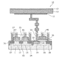
- FIG. 2A is a cross-sectional view illustrating an example of a configuration of a pixel according to the embodiment.
- the pixel 10 of the solid-state imaging device according to the present embodiment photoelectrically converts the n-type well 1 formed on the semiconductor substrate and the incident light formed above the semiconductor substrate.
- a transparent electrode such as ITO or ZnO is used in order to allow light to enter the photoelectric conversion layer 13.
- the n-type well 1 formed on the semiconductor substrate is used, but a p-type well formed on the semiconductor substrate may be used.
- n type and p type are interchanged as the conductivity type of the impurity described below.
- the electric charges generated in the photoelectric conversion layer 13 are transferred to the transparent electrode 12 by applying a positive voltage of about 10 V to transfer holes through the metal electrode 11 and accumulated in the p-type charge accumulation region 14.
- the charge storage region 14 also serves as an active region of the reset transistor 16, and when the reset transistor 16 is turned on, the potential of the charge storage region 14 is reset.
- the charge storage region 14 is electrically separated from the amplification transistor 15 or the selection transistor 17 in the pixel by a separation region 31 made of n-type or STI (Shallow Trench Isolation).
- an n-type surface injection region 32 is provided above the charge accumulation region 14 to suppress leakage of leak current caused by many defects on the surface of the well 1 into the charge accumulation region 14.
- a contact injection region 34 for reducing contact resistance is provided at the interface between the contact 33 for transferring the charge from the photoelectric conversion layer 13 to the charge storage region 14 and the semiconductor substrate. Further, the surface injection region 32 is extended to the vicinity of the gate end of the reset transistor 16.
- the film thickness of the gate oxide film 36 of the reset transistor 16 is larger than the film thickness of the gate oxide film 25 of the amplification transistor 15. With this configuration, a high gate voltage can be applied to the reset transistor 16. Therefore, when the reset transistor 16 is turned off, it is possible to collect the same electrons as the majority carriers that bear the surface injection region 32 under the gate, the potential of the surface injection region 32 can be stabilized, and the leakage current can be reduced.
- the on-state voltage of the reset transistor 16 is about 0V
- the off-state voltage is about 3.8V.
- 1 / f noise can be suppressed by forming the gate oxide film 25 of the amplification transistor 15 to be thin.
- the thickness of the gate oxide film 27 of the selection transistor 17 is set to be the same as the thickness of the gate oxide film 25 of the amplification transistor 15. With this configuration, the voltage applied to the gate when the selection transistor 17 is turned on can be reduced, so that low power consumption is promoted.
- the same thickness as described above includes substantially the same thickness, that is, a manufacturing error.
- the thickness of the gate oxide film 25 of the amplification transistor 15 is, for example, in the range of about 3 nm to 6 nm.
- the film thickness of the gate oxide film 36 of the reset transistor 16 is, for example, about 4 nm to 13 nm.
- the film thickness of the gate oxide film 27 of the selection transistor 17 is, for example, in the range of about 3 nm to 6 nm.
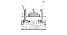
- FIG. 2B is a cross-sectional view illustrating an example of the configuration of the power supply circuit according to the embodiment.
- the film thickness of the gate oxide film 35 of the transistor constituting the power supply circuit 22 for applying a voltage to the transparent electrode 12 is larger than the film thickness of the gate oxide film 36 of the reset transistor 16. With this configuration, a high voltage can be applied to the transistors constituting the power supply circuit 22, and signal charges generated by the photoelectric conversion layer 13 can be transmitted to the charge storage region 14.
- the thickness of the gate oxide film 35 is preferably in the range of about 15 to 25 nm in order to apply about 10 V to the transparent electrode 12.
- the leakage current is improved by several tens of percent.
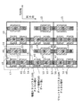
- FIG. 3 is a pixel plan view of the solid-state imaging device according to the first embodiment.
- the contact 33 of the charge storage region 14 in the pixel cannot be shared with the adjacent pixel 10 because the signal charge is mixed. Since the contact other than the contact 33 does not cause a problem of mixing of signal charges, it can be shared with the adjacent pixel 10, and the contact is shared with the pixel 10 adjacent in the vertical direction on the light receiving surface. As a result, the contact occupation area ratio per pixel is reduced, and the pixel size can be reduced.
- the amplification transistor 15 and the amplification transistor 15 of the pixel 10 adjacent in the vertical direction on the light receiving surface share the active region 54.
- the selection transistor 17 and the selection transistor 17 of the pixel 10 adjacent in the vertical direction on the light receiving surface share the active region 57.
- the gate length of the amplification transistor 15 sharing the active region can be secured while securing the gate length of the selection transistor 17, which is one of the noise components. f Noise can be reduced.
- the reset transistor 16 and the reset transistor 16 of the pixel 10 adjacent in the vertical direction on the light receiving surface share the active region 56.
- the gate length of the reset transistor 16 can be secured, and the on-characteristics of the reset transistor 16 having the charge accumulation region 14 as the active region can be secured.
- the gate length of the reset transistor 16 is longer than that of the amplification transistor 15. With this configuration, it is possible to reduce the on-characteristic variation of the reset transistor 16 having the charge accumulation region 14 as an active region, that is, the variation in threshold voltage, drain current, and the like depending on the gate length, while ensuring the driving capability of the amplification transistor 15.
- the potential of the charge storage region 14 can be stabilized. Therefore, the leak characteristics between pixels are uniform, and a clear image can be captured.
- the gate length of the amplification transistor is shortened and the mutual conductance gm is increased in inverse proportion to the length ⁇ L, the driving capability is increased and a signal can be transmitted to the output signal line 18 at high speed.
- the amplification transistor 15 and the selection transistor 17 are arranged in the same column. If the gate length is shortened while ensuring the on / off characteristics due to the gate voltage of the selection transistor 17, the gate length of the amplification transistor 15 can be increased, and 1 / f noise can also be reduced from Equation 1.
- the gate length of the amplification transistor 15 is preferably in the range of about 0.2 to 0.3 ⁇ m, for example.
- the gate length of the reset transistor 16 is, for example, in the range of about 0.2 to 0.5 ⁇ m.
- the gate length of the selection transistor 17 is, for example, in the range of about 0.1 to 0.5 ⁇ m.
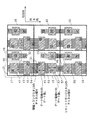
- FIG. 4 is a pixel plan view of the solid-state imaging device according to the second embodiment.
- the reset transistor 16 is formed separately from the amplification transistor 15 and the selection transistor 17 by the isolation region 31.
- the selection transistor 17 in the pixel shares a part of the active region 55 with the amplification transistor 15 in the same pixel, and the active region 56 of the reset transistor 16 in the pixel is in the same pixel.
- the pn junction area between the surface injection region 32 and the charge storage region 14 can be reduced, and pn junction leakage can be suppressed.
- the reset transistor 16 is disposed between the selection transistor 17 in the same pixel and the selection transistor 17 in the pixel adjacent in the horizontal direction on the light receiving surface.
- the reset transistor 16 may be disposed between the amplification transistor 15 in the same pixel and the amplification transistor 15 in the pixel adjacent in the horizontal direction on the light receiving surface (not shown).
- the channel width of the amplification transistor 15 is wider than the channel width of the reset transistor 16. From Equation 1, if the channel width of the amplification transistor 15 is increased, 1 / f noise of the amplification transistor 15 can be reduced. On the other hand, by reducing the channel width of the reset transistor 16, the pn junction area of the charge storage region 14 that also serves as the active region of the reset transistor 16 can be reduced, 1 / f noise and leakage current can be reduced, and noise components for signals A high-sensitivity image with reduced can be obtained. In addition, the transistor channel width can be increased to ensure high-speed driving in order to secure the operating current of the amplification transistor 15, and 1 / f noise, which is one of noise components, can be reduced.
- the channel width of the amplification transistor 15 is, for example, in the range of about 0.1 to 0.5 ⁇ m.
- the channel width of the reset transistor 16 is, for example, in the range of about 0.1 to 0.2 ⁇ m.
- the channel width of the selection transistor 17 is, for example, in the range of about 0.1 to 0.5 ⁇ m. It goes without saying that even when the pixel cell sizes are different, channel widths corresponding to different cell sizes can be derived by changing the cell size from 0.9 ⁇ m.
- the gate length of the gate electrode 47 of the selection transistor 17 is shorter than the gate length of the gate electrode 45 of the amplification transistor 15.
- the gate length of the amplification transistor 15 can be secured, and 1 / f noise, which is one of noise components, can be reduced.
- a solid-state imaging device with reduced leakage current and 1 / f noise can be manufactured. Further, a fine pixel size of about 1 ⁇ m can be realized, and high-speed charge readout can be performed.
- the solid-state imaging device according to the present invention has been described based on the first and second embodiments.
- the present invention is not limited to the first and second embodiments.
- various modifications conceivable by those skilled in the art in the first and second embodiments and forms constructed by combining components in different embodiments are also within the scope of the present invention. included.
- the solid-state imaging device is typically realized as an LSI that is an integrated circuit. These may be individually made into one chip, or may be made into one chip so as to include a part or all of them.
- circuits are not limited to LSI, and may be realized by a dedicated circuit or a general-purpose processor.
- An FPGA Field Programmable Gate Array
- reconfigurable processor that can reconfigure the connection and setting of circuit cells inside the LSI may be used.
- n-type and p-type such as impurity regions such as the surface implantation region 32, the contact implantation region 34, and the active regions 54 to 57, are illustrated to specifically describe the present invention, and these are inverted.
- the materials of the constituent elements shown above are all exemplified for specifically explaining the present invention, and the present invention is not limited to the exemplified materials.
- the connection relationship between the components is exemplified for specifically explaining the present invention, and the connection relationship for realizing the function of the present invention is not limited to this.
- MOS transistors In the above description, an example using MOS transistors is shown, but other transistors may be used.
- the solid-state imaging device of the present invention can be applied to a solid-state imaging device with a fine pixel size having a low noise characteristic with a stacked structure.
Landscapes
- Solid State Image Pick-Up Elements (AREA)
- Transforming Light Signals Into Electric Signals (AREA)
- Metal-Oxide And Bipolar Metal-Oxide Semiconductor Integrated Circuits (AREA)
Abstract
Le dispositif d'imagerie à semi-conducteurs de la présente invention comporte une pluralité de pixels disposés à deux dimensions (10). Chaque pixel (10) comporte : une électrode métallique (11) ; une couche de conversion photoélectrique (13) qui est formée sur l'électrode métallique, et qui convertit une lumière en signaux électriques ; une électrode transparente (12) formée sur la couche de conversion photoélectrique (13) ; une région d'accumulation de charges (14) qui est connectée électriquement à l'électrode métallique (11), et qui accumule la charge de la couche de conversion photoélectrique (13) ; un transistor d'amplification (15) qui fournit une tension de signal correspondant à la quantité de charges dans la région d'accumulation de charges (14) ; et un transistor de réinitialisation (16) qui réinitialise le potentiel de la région d'accumulation de charges (14). L'épaisseur de film d'un film d'oxyde de grille du transistor de réinitialisation (16) est plus épaisse que l'épaisseur de film d'un film d'oxyde de grille (25) du transistor d'amplification (15).
Priority Applications (4)
| Application Number | Priority Date | Filing Date | Title |
|---|---|---|---|
| CN201380032967.1A CN104412387B (zh) | 2012-06-27 | 2013-03-08 | 固体摄像装置 |
| JP2014522369A JP6108280B2 (ja) | 2012-06-27 | 2013-03-08 | 固体撮像装置 |
| US14/579,592 US9813651B2 (en) | 2012-06-27 | 2014-12-22 | Solid-state imaging device |
| US15/720,668 US9942506B2 (en) | 2012-06-27 | 2017-09-29 | Solid-state imaging device |
Applications Claiming Priority (2)
| Application Number | Priority Date | Filing Date | Title |
|---|---|---|---|
| JP2012-144763 | 2012-06-27 | ||
| JP2012144763 | 2012-06-27 |
Related Child Applications (1)
| Application Number | Title | Priority Date | Filing Date |
|---|---|---|---|
| US14/579,592 Continuation US9813651B2 (en) | 2012-06-27 | 2014-12-22 | Solid-state imaging device |
Publications (1)
| Publication Number | Publication Date |
|---|---|
| WO2014002330A1 true WO2014002330A1 (fr) | 2014-01-03 |
Family
ID=49782539
Family Applications (1)
| Application Number | Title | Priority Date | Filing Date |
|---|---|---|---|
| PCT/JP2013/001510 Ceased WO2014002330A1 (fr) | 2012-06-27 | 2013-03-08 | Dispositif d'imagerie à semi-conducteurs |
Country Status (4)
| Country | Link |
|---|---|
| US (2) | US9813651B2 (fr) |
| JP (1) | JP6108280B2 (fr) |
| CN (2) | CN104412387B (fr) |
| WO (1) | WO2014002330A1 (fr) |
Cited By (19)
| Publication number | Priority date | Publication date | Assignee | Title |
|---|---|---|---|---|
| JP2015207594A (ja) * | 2014-04-17 | 2015-11-19 | パナソニックIpマネジメント株式会社 | 固体撮像装置 |
| JP2016063216A (ja) * | 2014-09-12 | 2016-04-25 | パナソニックIpマネジメント株式会社 | 撮像装置 |
| JP2016127058A (ja) * | 2014-12-26 | 2016-07-11 | パナソニックIpマネジメント株式会社 | 撮像装置 |
| US9826016B2 (en) | 2015-02-24 | 2017-11-21 | Koninklijke Kpn N.V. | Fair adaptive streaming |
| CN107845649A (zh) * | 2016-09-20 | 2018-03-27 | 松下知识产权经营株式会社 | 摄像装置及其制造方法 |
| JP2018117347A (ja) * | 2017-01-19 | 2018-07-26 | パナソニックIpマネジメント株式会社 | 撮像装置 |
| JP2018186268A (ja) * | 2017-04-26 | 2018-11-22 | パナソニックIpマネジメント株式会社 | 撮像装置、および、カメラシステム |
| EP3435416A2 (fr) | 2017-07-24 | 2019-01-30 | Panasonic Intellectual Property Management Co., Ltd. | Dispositif d'imagerie |
| EP3439041A2 (fr) | 2017-07-31 | 2019-02-06 | Panasonic Intellectual Property Management Co., Ltd. | Dispositif d'imagerie |
| JP2019029643A (ja) * | 2017-07-31 | 2019-02-21 | パナソニックIpマネジメント株式会社 | 撮像装置 |
| JP2019192938A (ja) * | 2014-10-24 | 2019-10-31 | 株式会社半導体エネルギー研究所 | 撮像装置 |
| EP3576153A2 (fr) | 2018-05-31 | 2019-12-04 | Panasonic Intellectual Property Management Co., Ltd. | Dispositif d'imagerie |
| US10892286B2 (en) | 2018-05-31 | 2021-01-12 | Panasonic Intellectual Property Management Co., Ltd. | Imaging device |
| US10985197B2 (en) | 2018-10-15 | 2021-04-20 | Panasonic Intellectual Property Management Co., Ltd. | Imaging device |
| US11477262B2 (en) | 2014-02-13 | 2022-10-18 | Koninklijke Kpn N.V. | Requesting multiple chunks from a network node on the basis of a single request message |
| US11545525B2 (en) | 2019-09-05 | 2023-01-03 | Panasonic Intfllectual Property Management Co., Ltd. | Imaging device |
| US12176374B2 (en) | 2019-02-22 | 2024-12-24 | Panasonic Intellectual Property Management Co., Ltd. | Imaging device comprising isolation region between floating diffusion and another impurity region |
| US12342644B2 (en) | 2020-06-02 | 2025-06-24 | Panasonic Intellectual Property Management Co., Ltd. | Imaging apparatus |
| US12376391B2 (en) | 2019-09-26 | 2025-07-29 | Panasonic Intellectual Property Management Co., Ltd. | Imaging device |
Families Citing this family (4)
| Publication number | Priority date | Publication date | Assignee | Title |
|---|---|---|---|---|
| JP6179865B2 (ja) | 2012-06-26 | 2017-08-16 | パナソニックIpマネジメント株式会社 | 固体撮像装置及びその製造方法 |
| JP2019087939A (ja) * | 2017-11-09 | 2019-06-06 | キヤノン株式会社 | 光電変換装置、電子機器、輸送機器および光電変換装置の駆動方法 |
| JP7598710B2 (ja) * | 2020-05-26 | 2024-12-12 | 株式会社ジャパンディスプレイ | 検出装置 |
| JP7479203B2 (ja) * | 2020-06-04 | 2024-05-08 | キヤノン株式会社 | 発光装置、表示装置、光電変換装置、電子機器、照明装置、移動体およびウェアラブルデバイス |
Citations (5)
| Publication number | Priority date | Publication date | Assignee | Title |
|---|---|---|---|---|
| JP2006196884A (ja) * | 2004-12-16 | 2006-07-27 | Matsushita Electric Ind Co Ltd | 固体撮像装置 |
| JP2008124395A (ja) * | 2006-11-15 | 2008-05-29 | Matsushita Electric Ind Co Ltd | 固体撮像装置 |
| JP2011216728A (ja) * | 2010-03-31 | 2011-10-27 | Fujifilm Corp | 固体撮像素子の製造方法 |
| WO2012005010A1 (fr) * | 2010-07-09 | 2012-01-12 | パナソニック株式会社 | Dispositif d'imagerie à semi-conducteur |
| JP2012060076A (ja) * | 2010-09-13 | 2012-03-22 | Panasonic Corp | 固体撮像装置およびその製造方法 |
Family Cites Families (14)
| Publication number | Priority date | Publication date | Assignee | Title |
|---|---|---|---|---|
| EP1463306B8 (fr) * | 2003-03-25 | 2009-11-11 | Panasonic Corporation | Dispositif d'imagerie permettant d'empêcher la perte de detail des zones sombres |
| JP4403387B2 (ja) * | 2004-04-26 | 2010-01-27 | ソニー株式会社 | 固体撮像装置および固体撮像装置の駆動方法 |
| US8120077B2 (en) | 2004-12-16 | 2012-02-21 | Panasonic Corporation | Solid-state imaging device comprising doped channel stop at isolation regions to suppress noise |
| JP2006253316A (ja) * | 2005-03-09 | 2006-09-21 | Sony Corp | 固体撮像装置 |
| US7619671B2 (en) * | 2006-07-18 | 2009-11-17 | Aptina Imaging Corporation | Method, apparatus and system for charge injection suppression in active pixel sensors |
| JP5023808B2 (ja) * | 2007-05-24 | 2012-09-12 | ソニー株式会社 | 固体撮像装置およびカメラ |
| KR100882467B1 (ko) * | 2007-12-28 | 2009-02-09 | 주식회사 동부하이텍 | 이미지센서 및 그 제조방법 |
| JP5478043B2 (ja) | 2008-09-11 | 2014-04-23 | 富士フイルム株式会社 | 固体撮像素子及び撮像装置 |
| JP5444694B2 (ja) * | 2008-11-12 | 2014-03-19 | ソニー株式会社 | 固体撮像装置、その製造方法および撮像装置 |
| JP2010206173A (ja) * | 2009-02-06 | 2010-09-16 | Canon Inc | 光電変換装置およびカメラ |
| KR101584664B1 (ko) * | 2009-05-08 | 2016-01-13 | 삼성전자주식회사 | 씨모스 이미지 센서 |
| CN104393007A (zh) * | 2009-11-06 | 2015-03-04 | 株式会社半导体能源研究所 | 半导体装置 |
| JP5564918B2 (ja) * | 2009-12-03 | 2014-08-06 | ソニー株式会社 | 撮像素子およびカメラシステム |
| JP5470181B2 (ja) * | 2010-07-09 | 2014-04-16 | パナソニック株式会社 | 固体撮像装置 |
-
2013
- 2013-03-08 CN CN201380032967.1A patent/CN104412387B/zh active Active
- 2013-03-08 CN CN201711055697.2A patent/CN107833899B/zh active Active
- 2013-03-08 WO PCT/JP2013/001510 patent/WO2014002330A1/fr not_active Ceased
- 2013-03-08 JP JP2014522369A patent/JP6108280B2/ja active Active
-
2014
- 2014-12-22 US US14/579,592 patent/US9813651B2/en active Active
-
2017
- 2017-09-29 US US15/720,668 patent/US9942506B2/en active Active
Patent Citations (5)
| Publication number | Priority date | Publication date | Assignee | Title |
|---|---|---|---|---|
| JP2006196884A (ja) * | 2004-12-16 | 2006-07-27 | Matsushita Electric Ind Co Ltd | 固体撮像装置 |
| JP2008124395A (ja) * | 2006-11-15 | 2008-05-29 | Matsushita Electric Ind Co Ltd | 固体撮像装置 |
| JP2011216728A (ja) * | 2010-03-31 | 2011-10-27 | Fujifilm Corp | 固体撮像素子の製造方法 |
| WO2012005010A1 (fr) * | 2010-07-09 | 2012-01-12 | パナソニック株式会社 | Dispositif d'imagerie à semi-conducteur |
| JP2012060076A (ja) * | 2010-09-13 | 2012-03-22 | Panasonic Corp | 固体撮像装置およびその製造方法 |
Cited By (41)
| Publication number | Priority date | Publication date | Assignee | Title |
|---|---|---|---|---|
| US11477262B2 (en) | 2014-02-13 | 2022-10-18 | Koninklijke Kpn N.V. | Requesting multiple chunks from a network node on the basis of a single request message |
| JP2015207594A (ja) * | 2014-04-17 | 2015-11-19 | パナソニックIpマネジメント株式会社 | 固体撮像装置 |
| JP2016063216A (ja) * | 2014-09-12 | 2016-04-25 | パナソニックIpマネジメント株式会社 | 撮像装置 |
| JP2019212918A (ja) * | 2014-10-24 | 2019-12-12 | 株式会社半導体エネルギー研究所 | 撮像装置 |
| JP2019192938A (ja) * | 2014-10-24 | 2019-10-31 | 株式会社半導体エネルギー研究所 | 撮像装置 |
| JP2021103801A (ja) * | 2014-10-24 | 2021-07-15 | 株式会社半導体エネルギー研究所 | 撮像装置 |
| JP7122430B2 (ja) | 2014-10-24 | 2022-08-19 | 株式会社半導体エネルギー研究所 | 撮像装置 |
| JP2024103708A (ja) * | 2014-10-24 | 2024-08-01 | 株式会社半導体エネルギー研究所 | 撮像装置及び電子機器 |
| JP7705984B2 (ja) | 2014-10-24 | 2025-07-10 | 株式会社半導体エネルギー研究所 | 撮像装置及び電子機器 |
| JP2016127058A (ja) * | 2014-12-26 | 2016-07-11 | パナソニックIpマネジメント株式会社 | 撮像装置 |
| US9826016B2 (en) | 2015-02-24 | 2017-11-21 | Koninklijke Kpn N.V. | Fair adaptive streaming |
| US10446549B2 (en) | 2016-09-20 | 2019-10-15 | Panasonic Intellectual Property Management Co., Ltd. | Imaging device and manufacturing method thereof |
| CN107845649A (zh) * | 2016-09-20 | 2018-03-27 | 松下知识产权经营株式会社 | 摄像装置及其制造方法 |
| US10304828B2 (en) | 2016-09-20 | 2019-05-28 | Panasonic Intellectual Property Management Co., Ltd. | Imaging device and manufacturing method thereof |
| JP2018050035A (ja) * | 2016-09-20 | 2018-03-29 | パナソニックIpマネジメント株式会社 | 撮像装置およびその製造方法 |
| JP2018117347A (ja) * | 2017-01-19 | 2018-07-26 | パナソニックIpマネジメント株式会社 | 撮像装置 |
| US11070752B2 (en) | 2017-01-19 | 2021-07-20 | Panasonic Intellectual Property Management Co., Ltd. | Imaging device including first and second imaging cells and camera system |
| JP7133799B2 (ja) | 2017-04-26 | 2022-09-09 | パナソニックIpマネジメント株式会社 | 撮像装置、および、カメラシステム |
| US12074177B2 (en) | 2017-04-26 | 2024-08-27 | Panasonic Intellectual Property Management Co., Ltd. | Imaging device and camera system |
| JP2018186268A (ja) * | 2017-04-26 | 2018-11-22 | パナソニックIpマネジメント株式会社 | 撮像装置、および、カメラシステム |
| US10593714B2 (en) | 2017-07-24 | 2020-03-17 | Panasonic Intellectual Property Management Co., Ltd. | Imaging device |
| EP3896738A1 (fr) | 2017-07-24 | 2021-10-20 | Panasonic Intellectual Property Management Co., Ltd. | Dispositif d'imagerie |
| EP3435416A2 (fr) | 2017-07-24 | 2019-01-30 | Panasonic Intellectual Property Management Co., Ltd. | Dispositif d'imagerie |
| US10734432B2 (en) | 2017-07-31 | 2020-08-04 | Panasonic Intellectual Property Management Co., Ltd. | Imaging device |
| US11094734B2 (en) | 2017-07-31 | 2021-08-17 | Panasonic Intellectual Property Management Co., Ltd. | Imaging device |
| JP2019029643A (ja) * | 2017-07-31 | 2019-02-21 | パナソニックIpマネジメント株式会社 | 撮像装置 |
| EP3439041A2 (fr) | 2017-07-31 | 2019-02-06 | Panasonic Intellectual Property Management Co., Ltd. | Dispositif d'imagerie |
| US10892286B2 (en) | 2018-05-31 | 2021-01-12 | Panasonic Intellectual Property Management Co., Ltd. | Imaging device |
| US11195865B2 (en) | 2018-05-31 | 2021-12-07 | Panasonic Intellectual Property Management Co., Ltd. | Imaging device |
| US10615199B2 (en) | 2018-05-31 | 2020-04-07 | Panasonic Intellectual Property Management Co., Ltd. | Imaging device |
| EP3576153A2 (fr) | 2018-05-31 | 2019-12-04 | Panasonic Intellectual Property Management Co., Ltd. | Dispositif d'imagerie |
| US11532653B2 (en) | 2018-05-31 | 2022-12-20 | Panasonic Intellectual Property Management Co., Ltd. | Imaging device |
| US11631707B2 (en) | 2018-05-31 | 2023-04-18 | Panasonic Intellectual Property Management Co., Ltd. | Imaging device |
| US10985197B2 (en) | 2018-10-15 | 2021-04-20 | Panasonic Intellectual Property Management Co., Ltd. | Imaging device |
| US12046607B2 (en) | 2018-10-15 | 2024-07-23 | Panasonic Intellectual Property Management Co., Ltd. | Imaging device |
| US11715748B2 (en) | 2018-10-15 | 2023-08-01 | Panasonic Intellectual Property Management Co., Ltd. | Imaging device |
| US12176374B2 (en) | 2019-02-22 | 2024-12-24 | Panasonic Intellectual Property Management Co., Ltd. | Imaging device comprising isolation region between floating diffusion and another impurity region |
| US12193247B2 (en) | 2019-09-05 | 2025-01-07 | Panasonic Intellectual Property Management Co., Ltd. | Imaging device |
| US11545525B2 (en) | 2019-09-05 | 2023-01-03 | Panasonic Intfllectual Property Management Co., Ltd. | Imaging device |
| US12376391B2 (en) | 2019-09-26 | 2025-07-29 | Panasonic Intellectual Property Management Co., Ltd. | Imaging device |
| US12342644B2 (en) | 2020-06-02 | 2025-06-24 | Panasonic Intellectual Property Management Co., Ltd. | Imaging apparatus |
Also Published As
| Publication number | Publication date |
|---|---|
| US20150109503A1 (en) | 2015-04-23 |
| JP6108280B2 (ja) | 2017-04-05 |
| US20180048839A1 (en) | 2018-02-15 |
| CN104412387B (zh) | 2017-11-21 |
| JPWO2014002330A1 (ja) | 2016-05-30 |
| CN107833899B (zh) | 2021-11-19 |
| US9942506B2 (en) | 2018-04-10 |
| CN104412387A (zh) | 2015-03-11 |
| CN107833899A (zh) | 2018-03-23 |
| US9813651B2 (en) | 2017-11-07 |
Similar Documents
| Publication | Publication Date | Title |
|---|---|---|
| JP6108280B2 (ja) | 固体撮像装置 | |
| CN102017149B (zh) | 固态成像装置 | |
| CN102655158B (zh) | 固态成像器件 | |
| CN103946982B (zh) | 固体摄像装置 | |
| US11688748B2 (en) | Solid-state imaging apparatus | |
| JP2014045219A (ja) | 固体撮像装置 | |
| WO2014002362A1 (fr) | Dispositif de capture d'image à semi-conducteurs et procédé permettant de fabriquer ce dernier | |
| JPWO2012160802A1 (ja) | 固体撮像装置 | |
| CN111370433B (zh) | 摄像装置以及其制造方法 | |
| JP2016127058A (ja) | 撮像装置 | |
| US9472590B2 (en) | Solid-state image capturing device and manufacturing method thereof | |
| CN113016071A (zh) | 摄像装置 | |
| JP5388939B2 (ja) | 固体撮像素子 | |
| JP5709944B2 (ja) | 固体撮像装置 | |
| WO2025258400A1 (fr) | Transistor, appareil de détection de lumière et dispositif électronique | |
| JP2017027972A (ja) | 固体撮像装置および電子情報機器 | |
| JP2020074445A (ja) | 固体撮像装置 |
Legal Events
| Date | Code | Title | Description |
|---|---|---|---|
| 121 | Ep: the epo has been informed by wipo that ep was designated in this application |
Ref document number: 13809345 Country of ref document: EP Kind code of ref document: A1 |
|
| ENP | Entry into the national phase |
Ref document number: 2014522369 Country of ref document: JP Kind code of ref document: A |
|
| NENP | Non-entry into the national phase |
Ref country code: DE |
|
| 122 | Ep: pct application non-entry in european phase |
Ref document number: 13809345 Country of ref document: EP Kind code of ref document: A1 |