WO2014002361A1 - Dispositif de capture d'image à semi-conducteurs et procédé permettant de fabriquer ce dernier - Google Patents
Dispositif de capture d'image à semi-conducteurs et procédé permettant de fabriquer ce dernier Download PDFInfo
- Publication number
- WO2014002361A1 WO2014002361A1 PCT/JP2013/002958 JP2013002958W WO2014002361A1 WO 2014002361 A1 WO2014002361 A1 WO 2014002361A1 JP 2013002958 W JP2013002958 W JP 2013002958W WO 2014002361 A1 WO2014002361 A1 WO 2014002361A1
- Authority
- WO
- WIPO (PCT)
- Prior art keywords
- region
- gate electrode
- forming
- transistor
- conductivity type
- Prior art date
- Legal status (The legal status is an assumption and is not a legal conclusion. Google has not performed a legal analysis and makes no representation as to the accuracy of the status listed.)
- Ceased
Links
Images


Classifications
-
- H—ELECTRICITY
- H10—SEMICONDUCTOR DEVICES; ELECTRIC SOLID-STATE DEVICES NOT OTHERWISE PROVIDED FOR
- H10F—INORGANIC SEMICONDUCTOR DEVICES SENSITIVE TO INFRARED RADIATION, LIGHT, ELECTROMAGNETIC RADIATION OF SHORTER WAVELENGTH OR CORPUSCULAR RADIATION
- H10F39/00—Integrated devices, or assemblies of multiple devices, comprising at least one element covered by group H10F30/00, e.g. radiation detectors comprising photodiode arrays
- H10F39/10—Integrated devices
- H10F39/12—Image sensors
- H10F39/18—Complementary metal-oxide-semiconductor [CMOS] image sensors; Photodiode array image sensors
-
- H—ELECTRICITY
- H04—ELECTRIC COMMUNICATION TECHNIQUE
- H04N—PICTORIAL COMMUNICATION, e.g. TELEVISION
- H04N25/00—Circuitry of solid-state image sensors [SSIS]; Control thereof
- H04N25/60—Noise processing, e.g. detecting, correcting, reducing or removing noise
- H04N25/65—Noise processing, e.g. detecting, correcting, reducing or removing noise applied to reset noise, e.g. KTC noise related to CMOS structures by techniques other than CDS
-
- H—ELECTRICITY
- H04—ELECTRIC COMMUNICATION TECHNIQUE
- H04N—PICTORIAL COMMUNICATION, e.g. TELEVISION
- H04N25/00—Circuitry of solid-state image sensors [SSIS]; Control thereof
- H04N25/70—SSIS architectures; Circuits associated therewith
- H04N25/76—Addressed sensors, e.g. MOS or CMOS sensors
- H04N25/78—Readout circuits for addressed sensors, e.g. output amplifiers or A/D converters
-
- H—ELECTRICITY
- H10—SEMICONDUCTOR DEVICES; ELECTRIC SOLID-STATE DEVICES NOT OTHERWISE PROVIDED FOR
- H10D—INORGANIC ELECTRIC SEMICONDUCTOR DEVICES
- H10D84/00—Integrated devices formed in or on semiconductor substrates that comprise only semiconducting layers, e.g. on Si wafers or on GaAs-on-Si wafers
- H10D84/01—Manufacture or treatment
- H10D84/0123—Integrating together multiple components covered by H10D12/00 or H10D30/00, e.g. integrating multiple IGBTs
- H10D84/0126—Integrating together multiple components covered by H10D12/00 or H10D30/00, e.g. integrating multiple IGBTs the components including insulated gates, e.g. IGFETs
- H10D84/0135—Manufacturing their gate conductors
- H10D84/0142—Manufacturing their gate conductors the gate conductors having different shapes or dimensions
-
- H—ELECTRICITY
- H10—SEMICONDUCTOR DEVICES; ELECTRIC SOLID-STATE DEVICES NOT OTHERWISE PROVIDED FOR
- H10D—INORGANIC ELECTRIC SEMICONDUCTOR DEVICES
- H10D84/00—Integrated devices formed in or on semiconductor substrates that comprise only semiconducting layers, e.g. on Si wafers or on GaAs-on-Si wafers
- H10D84/01—Manufacture or treatment
- H10D84/0123—Integrating together multiple components covered by H10D12/00 or H10D30/00, e.g. integrating multiple IGBTs
- H10D84/0126—Integrating together multiple components covered by H10D12/00 or H10D30/00, e.g. integrating multiple IGBTs the components including insulated gates, e.g. IGFETs
- H10D84/0151—Manufacturing their isolation regions
-
- H—ELECTRICITY
- H10—SEMICONDUCTOR DEVICES; ELECTRIC SOLID-STATE DEVICES NOT OTHERWISE PROVIDED FOR
- H10D—INORGANIC ELECTRIC SEMICONDUCTOR DEVICES
- H10D84/00—Integrated devices formed in or on semiconductor substrates that comprise only semiconducting layers, e.g. on Si wafers or on GaAs-on-Si wafers
- H10D84/01—Manufacture or treatment
- H10D84/02—Manufacture or treatment characterised by using material-based technologies
- H10D84/03—Manufacture or treatment characterised by using material-based technologies using Group IV technology, e.g. silicon technology or silicon-carbide [SiC] technology
- H10D84/038—Manufacture or treatment characterised by using material-based technologies using Group IV technology, e.g. silicon technology or silicon-carbide [SiC] technology using silicon technology, e.g. SiGe
-
- H—ELECTRICITY
- H10—SEMICONDUCTOR DEVICES; ELECTRIC SOLID-STATE DEVICES NOT OTHERWISE PROVIDED FOR
- H10F—INORGANIC SEMICONDUCTOR DEVICES SENSITIVE TO INFRARED RADIATION, LIGHT, ELECTROMAGNETIC RADIATION OF SHORTER WAVELENGTH OR CORPUSCULAR RADIATION
- H10F39/00—Integrated devices, or assemblies of multiple devices, comprising at least one element covered by group H10F30/00, e.g. radiation detectors comprising photodiode arrays
- H10F39/011—Manufacture or treatment of image sensors covered by group H10F39/12
- H10F39/014—Manufacture or treatment of image sensors covered by group H10F39/12 of CMOS image sensors
-
- H—ELECTRICITY
- H10—SEMICONDUCTOR DEVICES; ELECTRIC SOLID-STATE DEVICES NOT OTHERWISE PROVIDED FOR
- H10F—INORGANIC SEMICONDUCTOR DEVICES SENSITIVE TO INFRARED RADIATION, LIGHT, ELECTROMAGNETIC RADIATION OF SHORTER WAVELENGTH OR CORPUSCULAR RADIATION
- H10F39/00—Integrated devices, or assemblies of multiple devices, comprising at least one element covered by group H10F30/00, e.g. radiation detectors comprising photodiode arrays
- H10F39/10—Integrated devices
- H10F39/12—Image sensors
- H10F39/191—Photoconductor image sensors
-
- H—ELECTRICITY
- H10—SEMICONDUCTOR DEVICES; ELECTRIC SOLID-STATE DEVICES NOT OTHERWISE PROVIDED FOR
- H10F—INORGANIC SEMICONDUCTOR DEVICES SENSITIVE TO INFRARED RADIATION, LIGHT, ELECTROMAGNETIC RADIATION OF SHORTER WAVELENGTH OR CORPUSCULAR RADIATION
- H10F39/00—Integrated devices, or assemblies of multiple devices, comprising at least one element covered by group H10F30/00, e.g. radiation detectors comprising photodiode arrays
- H10F39/80—Constructional details of image sensors
- H10F39/803—Pixels having integrated switching, control, storage or amplification elements
-
- H—ELECTRICITY
- H10—SEMICONDUCTOR DEVICES; ELECTRIC SOLID-STATE DEVICES NOT OTHERWISE PROVIDED FOR
- H10F—INORGANIC SEMICONDUCTOR DEVICES SENSITIVE TO INFRARED RADIATION, LIGHT, ELECTROMAGNETIC RADIATION OF SHORTER WAVELENGTH OR CORPUSCULAR RADIATION
- H10F39/00—Integrated devices, or assemblies of multiple devices, comprising at least one element covered by group H10F30/00, e.g. radiation detectors comprising photodiode arrays
- H10F39/80—Constructional details of image sensors
- H10F39/803—Pixels having integrated switching, control, storage or amplification elements
- H10F39/8033—Photosensitive area
-
- H—ELECTRICITY
- H10—SEMICONDUCTOR DEVICES; ELECTRIC SOLID-STATE DEVICES NOT OTHERWISE PROVIDED FOR
- H10F—INORGANIC SEMICONDUCTOR DEVICES SENSITIVE TO INFRARED RADIATION, LIGHT, ELECTROMAGNETIC RADIATION OF SHORTER WAVELENGTH OR CORPUSCULAR RADIATION
- H10F39/00—Integrated devices, or assemblies of multiple devices, comprising at least one element covered by group H10F30/00, e.g. radiation detectors comprising photodiode arrays
- H10F39/80—Constructional details of image sensors
- H10F39/803—Pixels having integrated switching, control, storage or amplification elements
- H10F39/8037—Pixels having integrated switching, control, storage or amplification elements the integrated elements comprising a transistor
-
- H—ELECTRICITY
- H10—SEMICONDUCTOR DEVICES; ELECTRIC SOLID-STATE DEVICES NOT OTHERWISE PROVIDED FOR
- H10F—INORGANIC SEMICONDUCTOR DEVICES SENSITIVE TO INFRARED RADIATION, LIGHT, ELECTROMAGNETIC RADIATION OF SHORTER WAVELENGTH OR CORPUSCULAR RADIATION
- H10F39/00—Integrated devices, or assemblies of multiple devices, comprising at least one element covered by group H10F30/00, e.g. radiation detectors comprising photodiode arrays
- H10F39/80—Constructional details of image sensors
- H10F39/807—Pixel isolation structures
-
- H—ELECTRICITY
- H10—SEMICONDUCTOR DEVICES; ELECTRIC SOLID-STATE DEVICES NOT OTHERWISE PROVIDED FOR
- H10P—GENERIC PROCESSES OR APPARATUS FOR THE MANUFACTURE OR TREATMENT OF DEVICES COVERED BY CLASS H10
- H10P30/00—Ion implantation into wafers, substrates or parts of devices
- H10P30/20—Ion implantation into wafers, substrates or parts of devices into semiconductor materials, e.g. for doping
- H10P30/22—Ion implantation into wafers, substrates or parts of devices into semiconductor materials, e.g. for doping using masks
Definitions
- the present invention relates to a solid-state imaging device and a manufacturing method thereof.
- MOS Metal-Oxide-Semiconductor
- solid-state imaging devices are mounted on mobile device cameras, in-vehicle cameras, surveillance cameras, and the like. These solid-state imaging devices are required to have a high-resolution imaging capability, and the solid-state imaging devices need to be miniaturized and have a large number of pixels.
- the size of the photodiode is also reduced due to pixel miniaturization.
- the sensitivity of the pixel decreases due to a decrease in the saturation signal amount and a decrease in the aperture ratio.
- a so-called insulation isolation method using a LOCOS (Local Oxidation of Silicon) isolation method or an STI (Shallow Trench Isolation) isolation method is used as a method for forming element isolation in the solid-state imaging device.
- STI forms a trench in the upper part of a semiconductor substrate, and embeds a silicon oxide film in the formed trench to constitute element isolation. Defects and interface states or stress caused by etching damage during the formation of trenches cause leakage current. The charge due to the leakage current is indistinguishable from the signal charge photoelectrically converted by the photodiode, and thus becomes noise and degrades the performance of the image sensor.
- Patent Document 1 As one method for suppressing leakage current, a method of forming an element isolation region with an impurity semiconductor layer is known (see, for example, Patent Document 1).
- the element isolation region in contact with the n-type semiconductor region serving as the floating diffusion (FD) portion is formed by STI, and the element isolation region other than the region in contact with the FD portion is p.
- a diffusion element isolation region of the mold is formed.
- the element isolation region in contact with the n-type semiconductor region serving as the FD portion is formed by STI, the capacitance formed between the n-type semiconductor region of the FD portion and the semiconductor substrate is reduced.
- the element isolation region other than the region in contact with the FD portion is formed of a p-type diffusion element isolation region, leakage current can be suppressed.
- a stacked solid-state imaging device is formed by stacking a photoelectric conversion film above a semiconductor substrate, that is, on the outermost surface. Light is incident from above the laminated film, and charges generated by photoelectric conversion in the photoelectric conversion film are accumulated in a charge accumulation region (FD), and on a semiconductor substrate by a CCD (Charge-Coupled Device) circuit or a CMOS (Complementary-MOS) circuit. Read (for example, refer to Patent Document 2).
- CCD Charge-Coupled Device
- CMOS Complementary-MOS
- a pn junction serving as an FD that accumulates signal charges is formed on a semiconductor substrate.
- a contact for transmitting a signal charge photoelectrically converted by the photoelectric conversion film is electrically connected to the pn junction.
- the leakage current at the pn junction of the semiconductor substrate is large.
- the signal charge accumulation time in the FD is longer than that in the conventional MOS sensor, the sensitivity decrease due to the leakage current becomes more remarkable in the stacked solid-state imaging device.
- the solid-state imaging device described in Patent Document 1 has a problem of an increase in gate capacity.
- the increase in the gate capacitance causes a decrease in gain in the amplification transistor and causes a decrease in sensitivity.
- increase in the gate capacitance becomes a parasitic capacitance of the FD portion electrically connected to a gate electrode, since the total capacity C FD of the FD portion is increased, when converting the charges obtained by the photoelectric conversion to the signal voltage There is also a problem that the conversion efficiency is reduced.
- an STI is formed instead of a diffusion element isolation region in a region in contact with the FD portion.
- element isolation having the STI structure is insufficient as a countermeasure against the problem of leakage current.
- this is a serious problem in a stacked solid-state imaging device in which leakage current in the FD portion is a problem.
- the inventors of the present application have found that if diffusion element isolation is used in the element isolation region, the alignment budget becomes large and it is difficult to reduce the pixel size.
- an object of the present invention is to improve sensitivity by suppressing an increase in gate capacitance while suppressing deterioration in signal-to-noise ratio due to occurrence of leakage current.
- Another object of the present invention is to suppress variations in transistor characteristics and performance degradation due to a decrease in effective channel width by inhibiting diffusion of impurity ions from the diffusion element isolation into the channel region.
- Another object of the present invention is to reduce the alignment budget so that the pixels can be more easily miniaturized.
- the present invention does not have to solve all of the above objects, and only needs to achieve at least one object.
- the solid-state imaging device has a configuration in which the distance in the gate width direction in the diffusion element separation is larger in the channel region than in the source / drain region.
- a solid-state imaging device includes a first conductivity type semiconductor region and a plurality of unit pixel cells arranged in the semiconductor region.
- the unit pixel cell includes a photoelectric conversion unit and a photoelectric conversion unit.
- a second conductivity type impurity region for forming a storage diode for storing the signal charge generated in step with the semiconductor region, an amplification transistor formed in the semiconductor region and having a gate electrode electrically connected to the impurity region;
- a first isolation region formed in a region around the amplification transistor in the semiconductor region and introduced with an impurity of the first conductivity type.
- the amplification transistor includes a gate electrode and a first isolation region in the semiconductor region.
- a first conductivity type source region or a second conductivity type drain region formed between the channel region and a channel region formed below the gate electrode in the semiconductor region;
- the width direction of the spacing of the gate electrode in the range, a portion sandwiching the channel region is greater than the portion sandwiching the source or drain region.
- the interval in the width direction of the gate electrode in the first isolation region into which the impurity is introduced is larger in the portion sandwiching the channel region than in the portion sandwiching the source region or drain region. Therefore, since the amount of protrusion of the gate electrode to the channel region (gate protrusion amount) in the amplification transistor is reduced, the increase in the gate capacitance is suppressed while suppressing the deterioration of the signal-to-noise ratio value due to the occurrence of the leakage current. be able to. As a result, the sensitivity of the solid-state imaging device can be improved. In addition, since the gate protrusion amount is reduced, a reduction in effective channel width due to diffusion of impurity ions from the first isolation region is suppressed, so that variations in transistor characteristics and performance deterioration can be reduced.
- the first separation region may also be formed in a region around the impurity region.
- the impurity region which is the FD portion is insulated by the first isolation region made of the impurity semiconductor layer, the gate capacitance which is a parasitic capacitance of the FD portion is reduced. As a result, it is possible to achieve both the reduction of the total capacity C FD of the leakage suppression and FD portion. In particular, in a stacked solid-state imaging device in which leakage current in the FD portion is a big problem, a more remarkable effect is shown.
- the photoelectric conversion unit is formed above the semiconductor region, photoelectric conversion film that photoelectrically converts incident light, a transparent electrode formed above the photoelectric conversion film, the semiconductor region, and photoelectric conversion
- a pixel electrode formed between the pixel electrode and the impurity region; and the pixel electrode and the impurity region may be electrically connected to each other.
- the present invention can obtain more remarkable effects.
- the end surface in the width direction of the gate electrode and the end surface below the gate electrode in the first separation region may be the same surface.
- the amount of gate protrusion can be minimized.
- the reduction of the effective channel width can be suppressed, the sensitivity of the solid-state imaging device can be improved, and variations in transistor characteristics and performance deterioration can be further reduced.
- the impurity concentration of the first isolation region is set to be higher than the impurity concentration of the semiconductor region, and an impurity of the first conductivity type is introduced into the semiconductor region, so that adjacent unit pixel cells You may further provide the 2nd isolation
- the impurity concentration of the first isolation region and the impurity concentration of the second isolation region may be the same.
- the unit pixel cell has a reset transistor that resets the potential of the gate electrode of the amplification transistor, the channel region of the amplification transistor is made of the first conductivity type impurity, and the reset transistor The channel region may be made of a first conductivity type impurity.
- Vth threshold voltage
- the unit pixel cell has a reset transistor that resets the potential of the gate electrode of the amplification transistor, and the channel region of the amplification transistor is made of the second conductivity type impurity,
- the channel region may be made of a first conductivity type impurity.
- the threshold voltage of the reset transistor can be set high to reduce off-leakage, so that FD leakage can be reduced.
- the threshold voltage of the amplification transistor can be set low, it can be reliably driven in the saturation region.
- the method for manufacturing a solid-state imaging device includes a step of selectively forming a gate electrode on a semiconductor region of the first conductivity type, and a width of a region including the gate electrode on the semiconductor region by a lithography method. Forming a pattern smaller than the width of the gate electrode, using the gate electrode and the pattern as a mask, implanting a first conductivity type impurity into the semiconductor region, and removing the pattern Thereafter, a step of forming a source / drain region by selectively injecting a second conductivity type impurity into a region where the pattern in the semiconductor region has been formed is provided.
- an isolation region for element isolation is formed, so that the alignment budget can be reduced. As a result, pixel miniaturization can be realized more easily.
- the channel region of the amplification transistor and the amplification transistor are selectively implanted by selectively injecting the first conductivity type impurity into the semiconductor region before the step of forming the gate electrode.
- the channel region of the reset transistor may be formed larger than the gate width of the reset transistor.
- the channel regions of the amplification transistor and the reset transistor are formed before forming the gate electrode, there is a region where the threshold voltage is partially lowered directly under each gate electrode due to the influence of misalignment or the like. It can be prevented from being formed. As a result, a channel region having a uniform impurity concentration, that is, a threshold voltage can be reliably formed.
- the method for manufacturing a solid-state imaging device includes a step of forming a channel region of an amplification transistor by selectively injecting a second conductivity type impurity into a semiconductor region before the step of forming a gate electrode.
- the channel region of the amplification transistor may be formed smaller than the gate width of the amplification transistor, while the channel region of the reset transistor may be formed larger than the gate width of the reset transistor.
- the channel region can be reliably formed inside the gate width of the amplification transistor. As a result, it is possible to prevent a leak path between the source and drain regions from being formed outside the gate electrode.
- the method for manufacturing a solid-state imaging device includes a step of forming a channel region of an amplification transistor by selectively injecting a second conductivity type impurity into a semiconductor region before the step of forming a gate electrode.
- the channel region of the amplification transistor is formed larger than the gate width of the amplification transistor, and the channel region of the reset transistor is formed larger than the gate width of the reset transistor to form the isolation region.
- the impurity concentration of one conductivity type depends on the process for forming the channel region of the amplification transistor. It may be higher than the impurity concentration of the second conductivity type in.
- the conductivity type can be reversed by impurity implantation at the time of forming the isolation region. Therefore, it is possible to prevent a leak path between the source and drain regions from being formed outside the gate electrode. Further, since the resist pattern for forming the channel region can be expanded to the outside of the gate electrode, the margin during lithography can be expanded.
- the increase in gate capacitance can be suppressed while suppressing the deterioration of the signal-to-noise ratio due to the occurrence of leakage current, so that the sensitivity can be improved.
- variations in transistor characteristics and performance degradation can be suppressed, and pixel miniaturization can be performed more easily.
- FIG. 1 is a circuit diagram showing a solid-state imaging device according to the first embodiment.
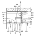
- FIG. 2 is a schematic cross-sectional view showing one unit pixel cell in the solid-state imaging device according to the first embodiment.
- FIG. 3 is a schematic diagram showing a potential of a portion along the line III-III in FIG. 2 in the unit pixel cell according to the first embodiment.
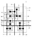
- FIG. 4 is a schematic plan view showing the configuration of the unit pixel cell according to the first embodiment.
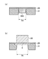
- 5A and 5B schematically show an active region and an element isolation region in the unit pixel cell according to the first embodiment, and FIG. 5A shows a cross section taken along the line Va-Va in FIG.
- FIG. 5B is a cross-sectional view taken along line Vb-Vb in FIG.
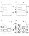
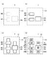
- FIG. 6A to FIG. 6D are plan views in order of steps showing the method for manufacturing the solid-state imaging device according to the first embodiment.
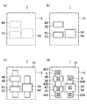
- FIG. 7A to FIG. 7D are plan views in the order of steps showing the method for manufacturing the solid-state imaging device according to the second embodiment.
- FIG. 8A to FIG. 8D are plan views in order of steps showing a method for manufacturing a solid-state imaging device according to a modification of the second embodiment.
- FIG. 1 shows a circuit configuration of the solid-state imaging device according to the first embodiment.
- the solid-state imaging device is a stacked solid-state imaging device, and is a photosensitive region composed of a plurality of unit pixel cells 13 arranged in a matrix on a semiconductor substrate. (Pixel region) and a drive circuit unit that sequentially drives the plurality of unit pixel cells 13 and extracts a photoelectrically converted signal.
- the drive circuit unit includes a vertical scanning unit (row scanning circuit) 15, a photoelectric conversion unit control line 16, a horizontal signal reading unit (column scanning circuit) 20, and a column signal processing unit (row signal) connected to the horizontal signal reading unit 20.
- Storage unit) 19 a vertical signal line (vertical signal line wiring) 17 connecting the column signal processing unit 19 and the unit pixel cell 13, a load unit 18 connected to the vertical signal line 17, and each unit pixel cell 13.
- An amplifier (feedback amplifier) 23 is included.
- the unit pixel cell (unit cell) 13 includes a photoelectric conversion unit 9, an amplification transistor 10, a reset transistor 11, and an address transistor (row selection transistor) 12.
- the photoelectric conversion unit 9 photoelectrically converts incident light, and generates and accumulates signal charges corresponding to the amount of incident light.
- the amplification transistor 10 outputs a signal voltage corresponding to the signal charge amount generated by the photoelectric conversion unit 9.
- the reset transistor 11 resets (initializes) the potential of the photoelectric conversion unit 9, that is, the gate electrode of the amplification transistor 10.
- the address transistor 12 selectively outputs a signal voltage from the unit pixel cell 13 in a predetermined row to the vertical signal line 17.
- the vertical scanning unit 15 scans the row of the unit pixel cells 13 in the vertical direction (column direction) by applying a row selection signal for controlling on / off of the address transistor 12 to the gate electrode of the address transistor 12. A row of unit pixel cells 13 for outputting a signal voltage to the vertical signal line 17 is selected. Further, the vertical scanning unit 15 selects a row of the unit pixel cells 13 on which the reset operation is performed by applying a reset signal for controlling on / off of the reset transistor 11 to the gate electrode of the reset transistor 11.
- the photoelectric conversion unit control line 16 is commonly connected to all the unit pixel cells 13 and applies the same positive constant voltage to all the photoelectric conversion units 9.
- the vertical signal line 17 is provided corresponding to each column of the unit pixel cells 13, is connected to the source region of the address transistor 12 in the unit pixel cell 13 of the corresponding column, and is arranged in the column direction to receive a signal voltage. Transmit in the column direction (vertical direction).
- the load unit 18 is connected to each vertical signal line 17 and constitutes a source follower circuit together with the amplification transistor 10.
- the column signal processing unit 19 performs noise suppression signal processing typified by correlated double sampling, AD conversion (analog-digital conversion), and the like.
- the column signal processing unit 19 is provided corresponding to each vertical signal line 17 and connected to the corresponding vertical signal line 17.
- the horizontal signal reading unit 20 sequentially reads signals from a plurality of column signal processing units 19 arranged in the horizontal direction (row direction) to a horizontal common signal line (not shown).
- the power supply wiring 21 is connected to each drain region of the amplification transistor 10 and wired in the vertical direction of the unit pixel cell 13 in the photosensitive region (up and down direction in the drawing of FIG. 1). This is because the unit pixel cell 13 is addressed for each row, and therefore, if the power supply wiring 21 is wired in the row direction (horizontal direction), the pixel drive current in one row all flows into one wiring, and the voltage drop increases. It is.
- the power supply wiring 21 applies a source follower power supply voltage in common to the amplification transistors 10 of all the unit pixel cells 13.
- the differential amplifier 23 is provided corresponding to each column of the unit pixel cells 13.
- the output terminal of the differential amplifier 23 is connected to the drain region of the reset transistor 11 via the feedback line 24. Accordingly, the differential amplifier 23 receives the output value of the address transistor 12 at the negative terminal when the address transistor 12 and the reset transistor 11 are in a conductive state, and the gate potential of the amplification transistor 10 is set to a predetermined feedback voltage (differential). The feedback operation is performed so that the output voltage of the amplifier 23 is obtained. At this time, the output voltage value of the differential amplifier 23 is 0V or a positive voltage near 0V.
- the signal charges photoelectrically converted by the photoelectric conversion unit 9 are amplified by the amplification transistors 10, respectively. 12 to the vertical signal line 17.
- the output signal charge is stored as an electrical signal in the column signal processing unit 19 and then selected and output by the horizontal signal reading unit 20.
- the signal charge in the unit pixel cell 13 that has output the signal is discharged by turning on the reset transistor 11.
- a large thermal noise called kTC noise is generated from the reset transistor 11. This thermal noise remains even when the reset transistor 11 is turned off and signal charge accumulation is started. Therefore, in order to suppress this thermal noise, the output value of the vertical signal line 17 is inverted and amplified by the differential amplifier 23, and the inverted and amplified signal is fed back to the drain region of the reset transistor 11 via the feedback line 24. .
- thermal noise generated in the reset transistor 11 can be suppressed by negative feedback control.
- it is an AC component of thermal noise that is fed back to the drain region of the reset transistor 11, and the DC component is a positive voltage in the vicinity of 0V as described above.
- FIG. 2 shows a schematic configuration of a cross section of one unit pixel cell 13 in the solid-state imaging device according to the present embodiment. Note that for simplification of description, three transistors are shown in one cross section although they are different from the actual structure.
- the unit pixel cell 13 includes, for example, a pixel circuit including three transistors formed on the semiconductor substrate 1 made of p-type silicon (Si), that is, an address transistor 12, an amplification transistor 10, and a reset transistor 11, and an element isolation region 31.
- Interlayer insulating films 14A, 14B and 14C sequentially stacked on the semiconductor substrate 1, a pixel electrode 5 formed on the interlayer insulating film 14C, and a photoelectric conversion film 6 formed on the pixel electrode 5.
- a photoelectric conversion part 9 including a transparent electrode 7 formed on the photoelectric conversion film 6.
- the reset transistor 11 includes n-type impurity regions 40A and 40B formed on the semiconductor substrate 1, and a gate insulating film 2A and a gate electrode 3A formed on the semiconductor substrate 1.
- the amplification transistor 10 is composed of n-type impurity regions 40C and 40D formed on the upper portion of the semiconductor substrate 1, and a gate insulating film 2B and a gate electrode 3B formed on the semiconductor substrate 1.
- the address transistor 12 is composed of n-type impurity regions 40D and 40E formed on the semiconductor substrate 1, and a gate insulating film 2C and a gate electrode 3C formed on the semiconductor substrate 1.
- the element isolation region 31 is composed of an impurity diffusion region that isolates and isolates the transistors 10, 11 and 12 from each other.
- the element isolation region 31 is formed between and around the amplification transistor 10 and the reset transistor 11 in the upper part of the semiconductor substrate 1, and electrically isolates the amplification transistor 10 and the reset transistor 11.
- the n-type impurity region 40A functions as a source region of the reset transistor 11, and the n-type impurity region 40B functions as a drain region of the reset transistor 11.
- the source / drain is reversed from the sensor using electrons as signal charges.
- the n-type impurity region 40C functions as the drain region of the amplification transistor 10.
- the n-type impurity region 40 ⁇ / b> D functions as a source region of the amplification transistor 10 and a drain region of the address transistor 12.
- the n-type impurity region 40E functions as the source region of the address transistor 12.
- the impurity concentration of the semiconductor substrate 1 is about 1 ⁇ 10 17 cm ⁇ 3 .
- the impurity concentration of the n-type impurity regions 40A, 40C, 40D and 40E is about 1 ⁇ 10 20 cm ⁇ 3 to 1 ⁇ 10 22 cm ⁇ 3 .
- the impurity concentration of the n-type impurity region 40B is about 1 ⁇ 10 18 cm ⁇ 3 .
- the film thicknesses of the gate insulating films 2A, 2B, and 2C formed below the gate electrodes 3A, 3B, and 3C are 4 nm to 10 nm, respectively.
- the photoelectric conversion film 6 is made of an organic material, amorphous silicon, or the like, is formed above the semiconductor substrate 1, and photoelectrically converts incident light from the outside.
- the pixel electrode 5 is formed on the surface of the photoelectric conversion film 6 on the semiconductor substrate 1 side, that is, on the back surface side of the photoelectric conversion film 6, in contact with the photoelectric conversion film 6, and collects signal charges generated in the photoelectric conversion film 6.
- the transparent electrode 7 is formed on the surface of the photoelectric conversion film 6 opposite to the pixel electrode 5, that is, on the surface of the photoelectric conversion film 6. A positive constant voltage is applied to the transparent electrode 7 via the photoelectric conversion unit control line 16, and signal charges generated in the photoelectric conversion film 6 can be read out to the pixel electrode 5.
- the amplification transistor 10 is a MOS transistor formed below the pixel electrode 5 in the semiconductor substrate 1.
- the amplification transistor 10 has a gate electrode 3 ⁇ / b> B connected to the pixel electrode 5, and outputs a signal voltage corresponding to the potential of the pixel electrode 5.
- the reset transistor 11 is a MOS transistor formed below the pixel electrode 5 in the semiconductor substrate 1.
- the reset transistor 11 is connected to the pixel electrode 5 and has a drain region (n-type impurity region 40 ⁇ / b> B) formed in a region between the gate electrode 3 ⁇ / b> A and the element isolation region 31 in the semiconductor substrate 1.
- the reset transistor 11 resets the potential of the gate electrode 3B of the amplification transistor 10 to a reset voltage, that is, a feedback voltage.
- the address transistor 12 is a MOS transistor formed below the pixel electrode 5 in the semiconductor substrate 1.
- the address transistor 12 is provided between the amplification transistor 10 and the vertical signal line 17, and outputs a signal voltage from the unit pixel cell 13 to the vertical signal line 17.
- the address transistor 12 is inserted between the source region of the amplification transistor 10 and the vertical signal line 17, but may be inserted between the drain region of the amplification transistor 10 and the power supply wiring 21.
- a contact plug 8 Between the gate electrode 3B of the amplification transistor 10 and the pixel electrode 5, and between the drain region (n-type impurity region) 40B of the reset transistor 11 and the pixel electrode 5, respectively, a contact plug 8, a wiring 26A, a plug 30A, The wiring 26B, the plug 30B, the wiring 26C, and the plug 30C are connected.
- a pn junction between the n-type impurity region 40B connected to the pixel electrode 5 and the semiconductor substrate 1 forms a parasitic diode (storage diode) that stores signal charges.
- the storage diode is also called a floating diffusion (FD) portion.
- FIG. 3 schematically shows the potential of the unit pixel cell 13, that is, the potential at the site along the line III-III in FIG.
- the positive voltage is applied to the transparent electrode 7 as described above, and the potential of the n-type impurity region 40 ⁇ / b> B that is a storage diode in a state where there is no signal (reset state). Is approximately 0 V with a slight reverse bias applied.
- the potential of the pixel electrode 5 and the n-type impurity region 40B is pulled in the positive direction by the positive voltage of the transparent electrode 7, if the n-type impurity region 40B is set to a low potential near 0V in this state, the n-type impurity Bias charge is injected into region 40B.
- the n-type impurity region 40B has a potential of about 0.1 V or higher and a low reverse bias.
- the reason for setting the value in the vicinity of 0 V is to reduce the reverse leakage current (dark current) flowing between the storage diode and the semiconductor substrate 1.
- the voltage changed to the positive side by the holes accumulated in the storage diode is transmitted to the gate electrode 3B of the amplification transistor 10.
- the signal transmitted to the gate electrode 3B and amplified by the amplification transistor 10 passes through the address transistor 12 and is output to the outside of the unit pixel cell 13, that is, to the vertical signal line 17. Thereafter, the signal charge stored in the storage diode is discharged by setting the reset transistor 11 to the ON state. At this time, the gate electrode 3 ⁇ / b> B of the amplification transistor 10 is reset to a voltage lower than the voltage applied to the transparent electrode 7.
- the signal charge accumulation time is one digit or more longer than that of a conventional MOS image sensor. For this reason, it is necessary to suppress leakage during storage and variations in operating characteristics of the amplification transistor 10.
- FIG. 4 shows a planar configuration of the unit pixel cell 13.
- the active regions of the amplification transistor 10 and the address transistor 12 are formed in the first active region 22 surrounded by the element isolation region 31 of the semiconductor substrate 1. .
- the active region of the reset transistor 11 is formed in the second active region 25 surrounded by the element isolation region 31 of the semiconductor substrate 1.
- the active region refers to a source region, a drain region, and a gate region (channel region).
- the vertical signal line 17 is connected to the source region of the address transistor 12, and the address signal line 28 is connected to the gate electrode 3C.
- a power supply wiring 21 is connected to the drain region of the amplification transistor 10.
- the drain region of the reset transistor 11 and the gate electrode 3 ⁇ / b> B of the amplification transistor 10 are electrically connected, and are drawn out above the semiconductor substrate 1 and connected to the photoelectric conversion unit 9.
- the reset transistor 11 is formed in the second active region 25 that is electrically isolated by the first active region 22 and the element isolation region 31.
- the source region of the reset transistor 11 is connected to the feedback line 24, and its gate electrode 3 A is connected to the reset signal line 27.
- the region where the leakage current becomes a problem is the reset transistor drain peripheral region 29 surrounding the drain region of the reset transistor 11.
- the first active region 22 and the second active region 25 are electrically separated between and around the first active region 22 and the second active region 25 in the semiconductor substrate 1.
- An element isolation region 31 is formed.
- the interval Sb between the portions sandwiching the channel region indicated by the Vb-Vb line is greater than the interval Sa between the portions sandwiching the drain region. Is also big.
- each layer and between each layer are designed.
- the alignment budget can be reduced.
- the unit pixel cell 13 can be miniaturized.
- the unit pixel cell 13 in order to miniaturize the unit pixel cell 13, it is necessary to reduce the area of the element isolation region 31 disposed between the first active region 22 and the second active region 25. For this purpose, it is necessary to design a pixel cell in consideration of exposure alignment accuracy, dimensional accuracy, mask accuracy, alignment accuracy between layers, and the like for each layer during pattern formation.
- the mask accuracy, exposure alignment accuracy, and resist dimensional accuracy of the layer forming the element isolation region 31, the mask accuracy of the layer forming the source / drain region, and the exposure The alignment budget for each layer in the two layers of the alignment accuracy and the resist dimensional accuracy and the alignment budget between these two layers may be considered.
- the mask accuracy, exposure alignment accuracy and resist dimensional accuracy of the layer forming the channel region below the gate electrode 3B, and the layer forming the gate electrode 3B may be considered. That is, in the structure according to the present embodiment, the alignment budget of two layers may be considered in each region corresponding to the Va-Va line and the Vb-Vb line.
- the region corresponding to the Va-Va line is the same as in the present embodiment, but in the region corresponding to the Vb-Vb line, the gate Mask accuracy, exposure alignment accuracy and resist dimensional accuracy of the layer forming the channel region under the electrode, mask accuracy of the layer forming the element isolation region, exposure alignment accuracy and resist dimensional accuracy, and of the layer forming the gate electrode It is necessary to consider the alignment budget for each layer in the three layers of mask accuracy, exposure alignment accuracy, and resist dimension accuracy, and the alignment budget between these three layers. Thus, since the overall alignment budget increases, it is difficult to miniaturize the unit pixel cell as compared with the present embodiment.
- FIG. 5 shows a cross-sectional configuration of the amplification transistor 10 in the gate width direction.
- 5A shows a cross section taken along the line Va-Va in FIG. 4
- FIG. 5B shows a cross section taken along the line Vb-Vb in FIG.
- each transistor of the pixel circuit that is, the amplification transistor 10, the reset transistor 11, and the address transistor 12 is configured by an n-type MOS transistor is shown. Therefore, the forward doping in which p-type impurity ions are implanted is used for the channel region of each transistor.
- the channel region 4 has a region where both end portions in the gate width direction overlap with the element isolation region 31. It is necessary to secure.
- the channel region 4 it is desirable to design the channel region 4 so that the width in the gate width direction is larger than the width of the gate electrode 3B.
- the width of the channel region 4 is smaller than the width of the gate electrode 3B, a region where p-type impurity ion implantation for channel formation is not performed is formed in the region immediately below the gate electrode 3B. In this case, a region where the threshold voltage (Vth) of the transistor is low is formed, and there arises a problem that it becomes impossible to control to a desired threshold voltage.
- Vth threshold voltage
- each transistor (10, 11 and 12) of a pixel circuit on a semiconductor substrate 1 made of p-type silicon (Si) by lithography.
- the resist pattern is formed.
- p-type impurity ions are ion-implanted under predetermined implantation conditions using the formed resist pattern as a mask, thereby forming the channel regions 4A, 4B and 4C.
- a desired threshold voltage can be obtained for each transistor of the pixel circuit.
- the channel regions 4A, 4B, and 4C are formed to have a width larger than that of the gate electrodes 3A, 3B, and 3C formed thereon.
- gate oxidation is performed on the main surface of the semiconductor substrate 1 by, for example, an ISSG (In Situ Steam Steam Generation) method or the like to form a gate insulating film made of silicon oxide (not shown). ).
- a gate forming film made of, for example, polysilicon is deposited on the gate insulating film by a chemical vapor deposition (CVD) method.
- CVD chemical vapor deposition
- a resist pattern for forming a gate electrode is formed on the gate forming film by lithography.
- gate electrodes 3A, 3B, and 3C are formed from the gate formation film by a dry etching method using the resist pattern as a mask.
- the channel regions 4A, 4B, and 4C of the transistors are formed, respectively, so that the gate electrodes 3A, 3B, and 3C are directly under the influence of misalignment. It is possible to prevent a region where the threshold voltage is partially lowered from being formed. As a result, a channel region having a uniform impurity concentration, that is, a threshold voltage can be reliably formed.
- a resist pattern for masking the source / drain regions of each transistor in the pixel circuit is formed by lithography, and then, using the formed resist pattern as a mask, predetermined implantation conditions are formed.
- the element isolation region 31 is formed by ion implantation of p-type impurity ions. At this time, p-type impurity ions for forming an element isolation region are not directly implanted directly under the gate electrodes 3A, 3B, and 3C. Therefore, the element isolation region 31 is formed so as to surround the source / drain region and the channel region, and thus has a shape located on both sides of the source / drain region and the channel region in the gate width direction.
- the end face in the gate width direction of the element isolation region 31 may be located at a location away from the channel region.
- the end surface in the gate width direction of the gate electrode 3A and the like and the end surface of the element isolation region 31 form the same surface.
- the term “same surface” as used herein may be approximately the same surface because a deviation of about several tens of nanometers due to thermal diffusion of impurity ions is allowed.
- p-type impurities are also formed in regions below the gate electrodes 3A, 3B, and 3C, respectively. It is possible to implant ions. However, in this case, the width of the diffusion layer in the source / drain region is similarly reduced. For this reason, as shown in FIG. 5A, the channel region 4 is larger than the interval Sa between the n-type impurity regions 40D in the gate width direction of the first active region 22 in the element isolation region 31. There is no change in the relationship that the interval Sb between the portions sandwiching the is larger.
- a resist pattern that opens the source / drain formation region of each transistor of the pixel circuit is formed by lithography.
- n-type impurity regions 40A, 40B, 40C, 40D, and 40E are respectively implanted by ion-implanting n-type impurity ions under predetermined implantation conditions using the formed resist pattern and the gate electrodes 3A, 3B, and 3C as masks.
- so-called gate implantation in which n-type impurity ions are implanted into each of the gate electrodes 3A, 3B, and 3C may be performed.
- the gate implantation may be performed after depositing a gate forming film made of polysilicon in the step shown in FIG. 6B.
- the n-type impurity regions 40A, 40B, 40C, 40D, and 40E are formed in a lump.
- another mask is used and lithography and impurity ion implantation are performed.
- the n-type impurity regions 40A, 40C, 40D, and 40E and the n-type impurity region 40B are preferably formed separately by a method.
- an interlayer insulating film made of silicon oxide or the like is formed on the semiconductor substrate 1 by the CVD method so as to cover the gate electrodes 3A, 3B, and 3C.
- a resist pattern for forming a contact hole is formed on the interlayer insulating film by lithography. Using the formed resist pattern as a mask, dry etching is performed to form contact holes on the gate electrodes 3A, 3B, and 3C and on the n-type impurity regions 40A, 40B, 40C, and 40E, respectively.
- n-type impurity ions are ion-implanted through the formed contact holes, thereby exposing the gate electrodes 3A, 3B and 3C and the upper portions of the n-type impurity regions 40A, 40B, 40C and 40E exposed from the contact holes.
- An n + -type impurity region is formed in (not shown).
- annealing for activating the implanted impurity ions is performed to reduce the resistance of each.
- a polysilicon film containing an n + type impurity is deposited on the interlayer insulating film so as to bury each contact hole by a CVD method or the like. Thereafter, the deposited polysilicon film is etched back or polished by a chemical mechanical polishing (CMP) method to form contact plugs 8 respectively.
- CMP chemical mechanical polishing
- a wiring 26A connected to the contact plug 8, a plug 30A connected to the wiring 26A, a wiring 26B connected to the plug 30A, a plug 30B connected to the wiring 26B, A wiring 26C connected to the plug 30B and a plug 30C connected to the wiring 26C are sequentially formed while laminating the interlayer insulating films 14A, 14B, and 14C.
- the pixel electrode 5, the photoelectric conversion film 6, the transparent electrode 7, the protective film (not shown), the color filter (not shown), and the lens (not shown) connected to the plug 30C on the interlayer insulating film 14C. are sequentially formed, so that the solid-state imaging device shown in FIG. 2 is formed. Note that these manufacturing methods are the same as the manufacturing method of the conventional stacked solid-state imaging device, and thus detailed description thereof is omitted.
- the element isolation region in contact with the n-type semiconductor region constituting the storage diode portion (FD portion) is formed by the p-type diffusion element isolation region. . For this reason, the leakage current from the FD portion is suppressed, and the occurrence of dark current and white spots can be suppressed.
- the p-type diffusion element isolation region is formed using the formed gate electrode as a mask after forming the gate electrode, the influence of impurity diffusion from the diffusion element isolation region to the channel region can be reduced. it can. Thereby, a desired channel width can be ensured, and variations in threshold voltage (Vth) and noise such as 1 / f noise can be reduced. As a result, a solid-state imaging device with an improved S / N ratio value can be realized.
- the gate protrusion amount can be minimized in consideration of the overlap with the channel region in the gate electrode. For this reason, an increase in gate capacitance, which is a problem in the conventional stacked solid-state imaging device, is suppressed, the conversion efficiency of photoelectric conversion can be increased, and the sensitivity of the solid-state imaging device can be improved.
- This embodiment is different from the first embodiment in that a channel region is formed by n-type impurity ion implantation, so-called counter-doping, in order to obtain a low threshold n-type transistor.
- the second embodiment is different from the first embodiment in that the channel region into which n-type impurity ions are implanted is smaller than the gate width. Thereby, it is possible to prevent a leak path between the source and drain regions from being formed outside the gate electrode.
- a resist pattern for forming a channel region of each transistor (10, 12) of the pixel circuit is formed on the semiconductor substrate 1 made of p-type silicon by lithography, for example. To do. At this time, the widths of the channel regions 4B and 4C are formed to be smaller than the widths of the gate electrodes 3B and 3C formed thereon, respectively. Thereafter, n-type impurity ions are ion-implanted under predetermined implantation conditions using the formed resist pattern as a mask, thereby forming channel regions 4B and 4C, respectively. Subsequently, a resist pattern for forming a channel region of the transistor (11) is formed.
- the width of the channel region 4A is formed to be larger than the width of the gate electrode 3A formed thereon as in the first embodiment.
- p-type impurity ions are ion-implanted under predetermined implantation conditions, thereby forming a channel region 4A.
- a desired threshold voltage can be obtained for each transistor of the pixel circuit.
- a gate insulating film (not shown) made of silicon oxide is formed on the main surface of the semiconductor substrate 1, for example, by performing gate oxidation by an ISSG method or the like.
- a gate forming film made of, for example, polysilicon is deposited on the gate insulating film by a CVD method.
- a resist pattern for forming a gate electrode is formed on the gate forming film by lithography.
- gate electrodes 3A, 3B, and 3C are formed from the gate formation film by a dry etching method using the resist pattern as a mask.
- the channel regions 4B and 4C are different from the first manufacturing method in that the channel regions 4B and 4C are included in the gate electrodes 3B and 3C in plan view in the gate width direction of the channel regions 4B and 4C.
- a resist pattern for masking the source / drain regions of each transistor in the pixel circuit is formed by lithography, and then, using the formed resist pattern as a mask, predetermined implantation conditions are formed.
- the element isolation region 31 is formed by ion implantation of p-type impurity ions. Thereby, the element isolation region 31 has a shape surrounding the source / drain region and the channel region.
- a resist pattern that opens the source / drain formation region of each transistor of the pixel circuit is formed by lithography.
- n-type impurity regions 40A, 40B, 40C, 40D and 40E are formed by ion-implanting n-type impurity ions under predetermined implantation conditions using the formed resist pattern and gate electrodes 3A, 3B and 3C as a mask. To do.
- channel doping is performed by p-type impurity ion implantation (forward doping) according to a desired threshold voltage, or n-type impurity ion implantation (counter). What is necessary is just to select whether it performs by dope), and is not limited to said combination.
- This modification is different from the second embodiment in that the n-type impurity ion implantation region for forming the channel region is larger than the gate width. Accordingly, since the resist pattern for forming the channel region can be expanded to the outside of the gate electrode, the margin at the time of lithography can be expanded.
- the amount of p-type impurity ion implantation for forming an element isolation region is larger than the amount of n-type impurity ion implantation for forming a channel region.
- the amplification transistor and the address transistor can be low threshold transistors.
- a resist pattern for forming a channel region of each transistor (10, 12) of the pixel circuit is formed on the semiconductor substrate 1 made of p-type silicon by lithography, for example. To do. At this time, the channel regions 4B and 4C are formed to have a width larger than that of the gate electrodes 3B and 3C, respectively. Thereafter, n-type impurity ions are ion-implanted under predetermined implantation conditions using the formed resist pattern as a mask, thereby forming channel regions 4B and 4C. Subsequently, a resist pattern for forming a channel region of the transistor (11) is formed. The channel region 4A is formed to have a width larger than that of the gate electrode 3A.
- p-type impurity ions are ion-implanted under predetermined implantation conditions, thereby forming a channel region 4A. Thereby, a desired threshold voltage can be obtained for each transistor of the pixel circuit.
- a gate insulating film (not shown) made of silicon oxide is formed on the main surface of the semiconductor substrate 1, for example, by performing gate oxidation by an ISSG method or the like.
- a gate forming film made of, for example, polysilicon is deposited on the gate insulating film by a CVD method.
- a resist pattern for forming a gate electrode is formed on the gate forming film by lithography.
- gate electrodes 3A, 3B, and 3C are formed from the gate formation film by a dry etching method using the resist pattern as a mask.
- the second manufacturing method is different in that the gate electrodes 3B and 3C are included in the channel regions 4B and 4C in plan view in the gate width direction of the channel regions 4B and 4C.
- a resist pattern for masking the source / drain regions of each transistor in the pixel circuit is formed by lithography, and then, using the formed resist pattern as a mask, predetermined implantation conditions are formed.
- the element isolation region 31 is formed by ion implantation of p-type impurity ions. Thereby, the element isolation region 31 has a shape surrounding the source / drain region and the channel region. At this time, the implantation amount of the p-type impurity ions for forming the element isolation region is made larger than the implantation amount of the n-type impurity ions for forming the channel region.
- the counter-doped n-type impurity ions can be inverted with the p-type impurity ions for forming the element isolation region. Therefore, it is possible to prevent the channel region from being formed around the gate electrodes 3B and 3C.
- a resist pattern that opens the source / drain formation region of each transistor of the pixel circuit is formed by lithography.
- n-type impurity regions 40A, 40B, 40C, 40D and 40E are formed by ion-implanting n-type impurity ions under predetermined implantation conditions using the formed resist pattern and gate electrodes 3A, 3B and 3C as a mask. To do.
- channel doping is performed by p-type impurity ion implantation (forward doping) according to a desired threshold voltage, or n-type impurity ion implantation (counter). What is necessary is just to select whether it performs by dope), and is not limited to said combination.
- the first conductivity type is p-type
- the second conductivity type is n-type
- the conductivity type of the semiconductor substrate 1 made of silicon is p-type and the transistors 10, 11 and 12 of the pixel circuit are n-channel type.
- the conductivity type of the semiconductor substrate 1 is n-type and the pixel circuit
- the transistors 10, 11 and 12 may be p-channel type.
- each transistor constituting the pixel circuit is a MOS transistor.
- the present invention is not limited to this as long as it is a field effect transistor (FET).
- the p-type semiconductor substrate includes a p-type semiconductor region such as a p-type well formed in the n-type semiconductor substrate.
- the solid-state imaging device is a stacked type that uses a photoelectric conversion film for the photoelectric conversion unit.
- the present invention is not limited to this, and a photodiode may be provided on the semiconductor substrate as the photoelectric conversion unit.
- the solid-state image pickup device and the manufacturing method thereof according to the present invention can realize a solid-state image pickup device that hardly deteriorates in image quality even when the pixel is miniaturized, and is useful for a digital camera or the like.
Landscapes
- Engineering & Computer Science (AREA)
- Multimedia (AREA)
- Signal Processing (AREA)
- Solid State Image Pick-Up Elements (AREA)
- Transforming Light Signals Into Electric Signals (AREA)
Abstract
La présente invention se rapporte à une cellule de pixels unitaires (13) qui comprend une partie de conversion photoélectrique (9), une région d'impureté de type n qui, conjointement avec une région semi-conductrice, forme une diode à accumulation dans laquelle s'accumule la charge de signal provenant de la partie de conversion photoélectrique, un transistor amplificateur (10) qui comprend une électrode de grille (3B) raccordée à la région d'impureté de type n, et une région de séparation d'élément (31) qui est formée dans la région périphérique du transistor amplificateur et dans laquelle ont été introduites des impuretés de type p. Le transistor amplificateur comprend une région source/drain de type n formée entre l'électrode de grille et la région de séparation d'élément, et une région de canal formée au niveau de la partie inférieure de l'électrode de grille. Un espace dans le sens de la largeur de la grille de la partie de la région de séparation d'électrode dans laquelle est insérée une région de canal, est plus large que celle de la partie dans laquelle est insérée une région source/drain.
Priority Applications (3)
| Application Number | Priority Date | Filing Date | Title |
|---|---|---|---|
| JP2014522382A JP6179865B2 (ja) | 2012-06-26 | 2013-05-08 | 固体撮像装置及びその製造方法 |
| US14/556,093 US9881960B2 (en) | 2012-06-26 | 2014-11-28 | Solid-state imaging device and method of manufacturing the device |
| US15/850,645 US10367025B2 (en) | 2012-06-26 | 2017-12-21 | Solid-state imaging device and method of manufacturing the device |
Applications Claiming Priority (2)
| Application Number | Priority Date | Filing Date | Title |
|---|---|---|---|
| JP2012-143129 | 2012-06-26 | ||
| JP2012143129 | 2012-06-26 |
Related Child Applications (2)
| Application Number | Title | Priority Date | Filing Date |
|---|---|---|---|
| US14/556,093 Continuation US9881960B2 (en) | 2012-06-26 | 2014-11-28 | Solid-state imaging device and method of manufacturing the device |
| US14556093 Continuation | 2015-11-28 |
Publications (1)
| Publication Number | Publication Date |
|---|---|
| WO2014002361A1 true WO2014002361A1 (fr) | 2014-01-03 |
Family
ID=49782563
Family Applications (1)
| Application Number | Title | Priority Date | Filing Date |
|---|---|---|---|
| PCT/JP2013/002958 Ceased WO2014002361A1 (fr) | 2012-06-26 | 2013-05-08 | Dispositif de capture d'image à semi-conducteurs et procédé permettant de fabriquer ce dernier |
Country Status (3)
| Country | Link |
|---|---|
| US (2) | US9881960B2 (fr) |
| JP (2) | JP6179865B2 (fr) |
| WO (1) | WO2014002361A1 (fr) |
Cited By (11)
| Publication number | Priority date | Publication date | Assignee | Title |
|---|---|---|---|---|
| US20160126276A1 (en) * | 2013-06-27 | 2016-05-05 | Sony Corporation | Solid-state imaging element, method of manufacturing the same, and imaging device |
| JP2016092081A (ja) * | 2014-10-30 | 2016-05-23 | キヤノン株式会社 | 光電変換装置および光電変換装置の製造方法 |
| JP2019012751A (ja) * | 2017-06-29 | 2019-01-24 | キヤノン株式会社 | 撮像装置、撮像システム、移動体、撮像装置の製造方法 |
| CN109300924A (zh) * | 2017-07-24 | 2019-02-01 | 松下知识产权经营株式会社 | 摄像装置 |
| USD851816S1 (en) | 2017-04-14 | 2019-06-18 | Curtis A. Roys | Lamp support |
| US10593714B2 (en) | 2017-07-24 | 2020-03-17 | Panasonic Intellectual Property Management Co., Ltd. | Imaging device |
| JPWO2021059882A1 (fr) * | 2019-09-26 | 2021-04-01 | ||
| US11165979B2 (en) | 2017-06-05 | 2021-11-02 | Panasonic Intellectual Property Management Co., Ltd. | Imaging device including semiconductor substrate and pixels |
| CN113658970A (zh) * | 2015-04-02 | 2021-11-16 | 松下知识产权经营株式会社 | 摄像装置 |
| JP2022112735A (ja) * | 2021-01-22 | 2022-08-03 | キヤノン株式会社 | 光電変換装置及び光検出システム |
| JP2023073519A (ja) * | 2018-05-31 | 2023-05-25 | パナソニックIpマネジメント株式会社 | 撮像装置 |
Families Citing this family (13)
| Publication number | Priority date | Publication date | Assignee | Title |
|---|---|---|---|---|
| JP6179865B2 (ja) * | 2012-06-26 | 2017-08-16 | パナソニックIpマネジメント株式会社 | 固体撮像装置及びその製造方法 |
| WO2014002362A1 (fr) * | 2012-06-26 | 2014-01-03 | パナソニック株式会社 | Dispositif de capture d'image à semi-conducteurs et procédé permettant de fabriquer ce dernier |
| WO2014002332A1 (fr) * | 2012-06-27 | 2014-01-03 | パナソニック株式会社 | Dispositif d'imagerie à semi-conducteurs |
| JP6541361B2 (ja) * | 2015-02-05 | 2019-07-10 | キヤノン株式会社 | 固体撮像装置 |
| JP2019033195A (ja) * | 2017-08-09 | 2019-02-28 | キヤノン株式会社 | 撮像装置の製造方法 |
| CN107749410B (zh) * | 2017-09-22 | 2019-08-09 | 京东方科技集团股份有限公司 | 环境光传感器、显示面板及显示装置 |
| CN110139047B (zh) * | 2018-02-08 | 2023-06-20 | 松下知识产权经营株式会社 | 摄像装置及相机系统、以及摄像装置的驱动方法 |
| JP2020021775A (ja) * | 2018-07-30 | 2020-02-06 | キヤノン株式会社 | 固体撮像装置及び撮像システム |
| JP2020113573A (ja) * | 2019-01-08 | 2020-07-27 | キヤノン株式会社 | 光電変換装置 |
| KR20210004595A (ko) * | 2019-07-05 | 2021-01-13 | 에스케이하이닉스 주식회사 | 이미지 센싱 장치 |
| US11100586B1 (en) | 2019-07-09 | 2021-08-24 | Wells Fargo Bank, N.A. | Systems and methods for callable options values determination using deep machine learning |
| JP7689307B2 (ja) * | 2020-01-30 | 2025-06-06 | パナソニックIpマネジメント株式会社 | 撮像装置 |
| TWI779943B (zh) * | 2021-12-01 | 2022-10-01 | 友達光電股份有限公司 | 感光裝置 |
Citations (4)
| Publication number | Priority date | Publication date | Assignee | Title |
|---|---|---|---|---|
| JP2009016810A (ja) * | 2007-06-04 | 2009-01-22 | Sony Corp | 半導体装置及びその製造方法 |
| JP2011114323A (ja) * | 2009-11-30 | 2011-06-09 | Sony Corp | 固体撮像装置とその製造方法、及び電子機器 |
| JP2011243704A (ja) * | 2010-05-17 | 2011-12-01 | Panasonic Corp | 固体撮像装置 |
| JP2012064822A (ja) * | 2010-09-17 | 2012-03-29 | Panasonic Corp | 固体撮像装置及びその製造方法 |
Family Cites Families (26)
| Publication number | Priority date | Publication date | Assignee | Title |
|---|---|---|---|---|
| JP3840203B2 (ja) * | 2002-06-27 | 2006-11-01 | キヤノン株式会社 | 固体撮像装置及び固体撮像装置を用いたカメラシステム |
| JP2006120710A (ja) * | 2004-10-19 | 2006-05-11 | Toshiba Corp | 固体撮像装置 |
| US8120077B2 (en) * | 2004-12-16 | 2012-02-21 | Panasonic Corporation | Solid-state imaging device comprising doped channel stop at isolation regions to suppress noise |
| JP2006294871A (ja) * | 2005-04-11 | 2006-10-26 | Matsushita Electric Ind Co Ltd | 固体撮像装置 |
| JP5320659B2 (ja) * | 2005-12-05 | 2013-10-23 | ソニー株式会社 | 固体撮像装置 |
| KR100790228B1 (ko) | 2005-12-26 | 2008-01-02 | 매그나칩 반도체 유한회사 | 시모스 이미지 센서 |
| US20080067589A1 (en) * | 2006-09-20 | 2008-03-20 | Akira Ito | Transistor having reduced channel dopant fluctuation |
| JP4420039B2 (ja) | 2007-02-16 | 2010-02-24 | ソニー株式会社 | 固体撮像装置 |
| JP2011508283A (ja) * | 2007-12-28 | 2011-03-10 | スリーエム イノベイティブ プロパティズ カンパニー | 光合成器 |
| US8115154B2 (en) * | 2008-08-01 | 2012-02-14 | Sony Corporation | Solid-state imaging device, method of producing the same, and imaging device |
| JP4444371B1 (ja) | 2009-09-01 | 2010-03-31 | 富士フイルム株式会社 | 撮像素子及び撮像装置 |
| JP5564874B2 (ja) * | 2009-09-25 | 2014-08-06 | ソニー株式会社 | 固体撮像装置、及び電子機器 |
| JP2011114036A (ja) * | 2009-11-24 | 2011-06-09 | Brookman Technology Inc | 絶縁ゲート型半導体素子及び絶縁ゲート型半導体集積回路 |
| JP2011114302A (ja) * | 2009-11-30 | 2011-06-09 | Sony Corp | 半導体素子の製造方法及び半導体素子、並びに固体撮像素子及び固体撮像装置 |
| JP5470181B2 (ja) * | 2010-07-09 | 2014-04-16 | パナソニック株式会社 | 固体撮像装置 |
| JP5530839B2 (ja) * | 2010-07-09 | 2014-06-25 | パナソニック株式会社 | 固体撮像装置 |
| JP2012060076A (ja) * | 2010-09-13 | 2012-03-22 | Panasonic Corp | 固体撮像装置およびその製造方法 |
| JP5960961B2 (ja) * | 2010-11-16 | 2016-08-02 | キヤノン株式会社 | 固体撮像素子及び撮像システム |
| US8471316B2 (en) * | 2011-09-07 | 2013-06-25 | Omnivision Technologies, Inc. | Isolation area between semiconductor devices having additional active area |
| US8883544B2 (en) * | 2012-05-04 | 2014-11-11 | Taiwan Semiconductor Manufacturing Company, Ltd. | Method of forming an image device |
| US9040341B2 (en) * | 2012-06-04 | 2015-05-26 | Taiwan Semiconductor Manufacturing Company, Ltd. | Image device and methods of forming the same |
| JP6179865B2 (ja) * | 2012-06-26 | 2017-08-16 | パナソニックIpマネジメント株式会社 | 固体撮像装置及びその製造方法 |
| WO2014002362A1 (fr) * | 2012-06-26 | 2014-01-03 | パナソニック株式会社 | Dispositif de capture d'image à semi-conducteurs et procédé permettant de fabriquer ce dernier |
| CN104412387B (zh) * | 2012-06-27 | 2017-11-21 | 松下知识产权经营株式会社 | 固体摄像装置 |
| US9196751B2 (en) * | 2013-03-14 | 2015-11-24 | Taiwan Semiconductor Manufacturing Co., Ltd. | Junction FET semiconductor device with dummy mask structures for improved dimension control and method for forming the same |
| JP2015088621A (ja) * | 2013-10-30 | 2015-05-07 | 株式会社東芝 | 固体撮像装置および固体撮像装置の製造方法 |
-
2013
- 2013-05-08 JP JP2014522382A patent/JP6179865B2/ja active Active
- 2013-05-08 WO PCT/JP2013/002958 patent/WO2014002361A1/fr not_active Ceased
-
2014
- 2014-11-28 US US14/556,093 patent/US9881960B2/en active Active
-
2017
- 2017-07-07 JP JP2017133675A patent/JP6541080B2/ja active Active
- 2017-12-21 US US15/850,645 patent/US10367025B2/en active Active
Patent Citations (4)
| Publication number | Priority date | Publication date | Assignee | Title |
|---|---|---|---|---|
| JP2009016810A (ja) * | 2007-06-04 | 2009-01-22 | Sony Corp | 半導体装置及びその製造方法 |
| JP2011114323A (ja) * | 2009-11-30 | 2011-06-09 | Sony Corp | 固体撮像装置とその製造方法、及び電子機器 |
| JP2011243704A (ja) * | 2010-05-17 | 2011-12-01 | Panasonic Corp | 固体撮像装置 |
| JP2012064822A (ja) * | 2010-09-17 | 2012-03-29 | Panasonic Corp | 固体撮像装置及びその製造方法 |
Cited By (27)
| Publication number | Priority date | Publication date | Assignee | Title |
|---|---|---|---|---|
| US9590003B2 (en) * | 2013-06-27 | 2017-03-07 | Sony Corporation | Solid-state imaging element, method of manufacturing the same, and imaging device |
| US10002902B2 (en) | 2013-06-27 | 2018-06-19 | Sony Semiconductor Solutions Corporation | Solid-state imaging element, method of manufacturing the same, and imaging device for reducing thickness of photoelectric conversion film |
| US20160126276A1 (en) * | 2013-06-27 | 2016-05-05 | Sony Corporation | Solid-state imaging element, method of manufacturing the same, and imaging device |
| US10276624B2 (en) | 2013-06-27 | 2019-04-30 | Sony Semiconductor Solutions Corporation | Solid-state imaging element, method of manufacturing the same, and imaging device |
| US20190252452A1 (en) * | 2013-06-27 | 2019-08-15 | Sony Semiconductor Solutions Corporation | Solid-state imaging element, method of manufacturing the same, and imaging device |
| US10593721B2 (en) | 2013-06-27 | 2020-03-17 | Sony Semiconductor Solutions Corporation | Solid-state imaging element, method of manufacturing the same, and imaging device |
| JP2016092081A (ja) * | 2014-10-30 | 2016-05-23 | キヤノン株式会社 | 光電変換装置および光電変換装置の製造方法 |
| CN113658970A (zh) * | 2015-04-02 | 2021-11-16 | 松下知识产权经营株式会社 | 摄像装置 |
| USD851816S1 (en) | 2017-04-14 | 2019-06-18 | Curtis A. Roys | Lamp support |
| US11165979B2 (en) | 2017-06-05 | 2021-11-02 | Panasonic Intellectual Property Management Co., Ltd. | Imaging device including semiconductor substrate and pixels |
| JP2019012751A (ja) * | 2017-06-29 | 2019-01-24 | キヤノン株式会社 | 撮像装置、撮像システム、移動体、撮像装置の製造方法 |
| JP7171170B2 (ja) | 2017-06-29 | 2022-11-15 | キヤノン株式会社 | 撮像装置、撮像システム、移動体、撮像装置の製造方法 |
| JP2019024075A (ja) * | 2017-07-24 | 2019-02-14 | パナソニックIpマネジメント株式会社 | 撮像装置 |
| CN109300924A (zh) * | 2017-07-24 | 2019-02-01 | 松下知识产权经营株式会社 | 摄像装置 |
| CN109300924B (zh) * | 2017-07-24 | 2023-11-03 | 松下知识产权经营株式会社 | 摄像装置 |
| US10593714B2 (en) | 2017-07-24 | 2020-03-17 | Panasonic Intellectual Property Management Co., Ltd. | Imaging device |
| TWI750351B (zh) * | 2017-07-24 | 2021-12-21 | 日商松下知識產權經營股份有限公司 | 拍攝裝置 |
| JP2023073519A (ja) * | 2018-05-31 | 2023-05-25 | パナソニックIpマネジメント株式会社 | 撮像装置 |
| JP7511193B2 (ja) | 2018-05-31 | 2024-07-05 | パナソニックIpマネジメント株式会社 | 撮像装置 |
| WO2021059882A1 (fr) * | 2019-09-26 | 2021-04-01 | パナソニックIpマネジメント株式会社 | Dispositif d'imagerie |
| JPWO2021059882A1 (fr) * | 2019-09-26 | 2021-04-01 | ||
| JP7668464B2 (ja) | 2019-09-26 | 2025-04-25 | パナソニックIpマネジメント株式会社 | 撮像装置 |
| US12376391B2 (en) | 2019-09-26 | 2025-07-29 | Panasonic Intellectual Property Management Co., Ltd. | Imaging device |
| JP2022112735A (ja) * | 2021-01-22 | 2022-08-03 | キヤノン株式会社 | 光電変換装置及び光検出システム |
| JP7414748B2 (ja) | 2021-01-22 | 2024-01-16 | キヤノン株式会社 | 光電変換装置及び光検出システム |
| JP2024026582A (ja) * | 2021-01-22 | 2024-02-28 | キヤノン株式会社 | 光電変換装置及び光検出システム |
| JP7583906B2 (ja) | 2021-01-22 | 2024-11-14 | キヤノン株式会社 | 光電変換装置及び光検出システム |
Also Published As
| Publication number | Publication date |
|---|---|
| JPWO2014002361A1 (ja) | 2016-05-30 |
| JP6541080B2 (ja) | 2019-07-10 |
| US20150123180A1 (en) | 2015-05-07 |
| US9881960B2 (en) | 2018-01-30 |
| JP6179865B2 (ja) | 2017-08-16 |
| US20180114811A1 (en) | 2018-04-26 |
| JP2017216462A (ja) | 2017-12-07 |
| US10367025B2 (en) | 2019-07-30 |
Similar Documents
| Publication | Publication Date | Title |
|---|---|---|
| JP6179865B2 (ja) | 固体撮像装置及びその製造方法 | |
| JP5426114B2 (ja) | 半導体装置及びその製造方法 | |
| CN103024295B (zh) | 固体拍摄装置及拍摄机 | |
| JP5493430B2 (ja) | 固体撮像装置とその製造方法、及び電子機器 | |
| JP5564909B2 (ja) | 固体撮像装置とその製造方法、及び電子機器 | |
| JP4224036B2 (ja) | フォトダイオード領域を埋め込んだイメージセンサ及びその製造方法 | |
| CN101488512B (zh) | 固态图像拾取装置 | |
| CN102683370B (zh) | 固体摄像装置及其制造方法以及电子装置 | |
| JP6960600B2 (ja) | 撮像装置およびその製造方法 | |
| JP3584196B2 (ja) | 受光素子及びそれを有する光電変換装置 | |
| US9711558B2 (en) | Imaging device with photoelectric converter | |
| JP6406585B2 (ja) | 撮像装置 | |
| WO2014002362A1 (fr) | Dispositif de capture d'image à semi-conducteurs et procédé permettant de fabriquer ce dernier | |
| CN101359675A (zh) | 固态图像捕获装置及其制造方法和电子信息装置 | |
| CN102169883A (zh) | 固态成像装置及其制造方法、电子设备 | |
| KR20120052875A (ko) | 고체 이미지 센서, 고체 이미지 센서의 제조 방법 및 촬상 시스템 | |
| CN102196198A (zh) | 固体摄像器件、其制造方法和驱动方法、以及电子装置 | |
| JP2013045879A (ja) | 半導体装置、半導体装置の製造方法、固体撮像装置、固体撮像装置の製造方法、電子機器 | |
| JP5407282B2 (ja) | 固体撮像装置とその製造方法、及び電子機器 | |
| JP2013045878A (ja) | 固体撮像装置、固体撮像装置の製造方法、電子機器 | |
| KR20070007666A (ko) | 이미지 센서 및 그 제조방법들 | |
| KR20140110844A (ko) | 고체 촬상 소자 및 전자 기기 | |
| JP5274118B2 (ja) | 固体撮像装置 | |
| CN116250248A (zh) | 固态摄像装置及其制造方法和电子设备 | |
| JP2012160750A (ja) | 光電変換装置 |
Legal Events
| Date | Code | Title | Description |
|---|---|---|---|
| 121 | Ep: the epo has been informed by wipo that ep was designated in this application |
Ref document number: 13809447 Country of ref document: EP Kind code of ref document: A1 |
|
| ENP | Entry into the national phase |
Ref document number: 2014522382 Country of ref document: JP Kind code of ref document: A |
|
| NENP | Non-entry into the national phase |
Ref country code: DE |
|
| 122 | Ep: pct application non-entry in european phase |
Ref document number: 13809447 Country of ref document: EP Kind code of ref document: A1 |