WO2014002597A1 - 炭化珪素半導体装置 - Google Patents
炭化珪素半導体装置 Download PDFInfo
- Publication number
- WO2014002597A1 WO2014002597A1 PCT/JP2013/061919 JP2013061919W WO2014002597A1 WO 2014002597 A1 WO2014002597 A1 WO 2014002597A1 JP 2013061919 W JP2013061919 W JP 2013061919W WO 2014002597 A1 WO2014002597 A1 WO 2014002597A1
- Authority
- WO
- WIPO (PCT)
- Prior art keywords
- layer
- semiconductor device
- conductivity type
- silicon carbide
- gate
- Prior art date
- Legal status (The legal status is an assumption and is not a legal conclusion. Google has not performed a legal analysis and makes no representation as to the accuracy of the status listed.)
- Ceased
Links
Images





Classifications
-
- H—ELECTRICITY
- H10—SEMICONDUCTOR DEVICES; ELECTRIC SOLID-STATE DEVICES NOT OTHERWISE PROVIDED FOR
- H10D—INORGANIC ELECTRIC SEMICONDUCTOR DEVICES
- H10D30/00—Field-effect transistors [FET]
- H10D30/80—FETs having rectifying junction gate electrodes
- H10D30/83—FETs having PN junction gate electrodes
-
- H—ELECTRICITY
- H10—SEMICONDUCTOR DEVICES; ELECTRIC SOLID-STATE DEVICES NOT OTHERWISE PROVIDED FOR
- H10D—INORGANIC ELECTRIC SEMICONDUCTOR DEVICES
- H10D12/00—Bipolar devices controlled by the field effect, e.g. insulated-gate bipolar transistors [IGBT]
-
- H—ELECTRICITY
- H10—SEMICONDUCTOR DEVICES; ELECTRIC SOLID-STATE DEVICES NOT OTHERWISE PROVIDED FOR
- H10D—INORGANIC ELECTRIC SEMICONDUCTOR DEVICES
- H10D12/00—Bipolar devices controlled by the field effect, e.g. insulated-gate bipolar transistors [IGBT]
- H10D12/01—Manufacture or treatment
- H10D12/031—Manufacture or treatment of IGBTs
-
- H—ELECTRICITY
- H10—SEMICONDUCTOR DEVICES; ELECTRIC SOLID-STATE DEVICES NOT OTHERWISE PROVIDED FOR
- H10D—INORGANIC ELECTRIC SEMICONDUCTOR DEVICES
- H10D12/00—Bipolar devices controlled by the field effect, e.g. insulated-gate bipolar transistors [IGBT]
- H10D12/01—Manufacture or treatment
- H10D12/031—Manufacture or treatment of IGBTs
- H10D12/032—Manufacture or treatment of IGBTs of vertical IGBTs
- H10D12/038—Manufacture or treatment of IGBTs of vertical IGBTs having a recessed gate, e.g. trench-gate IGBTs
-
- H—ELECTRICITY
- H10—SEMICONDUCTOR DEVICES; ELECTRIC SOLID-STATE DEVICES NOT OTHERWISE PROVIDED FOR
- H10D—INORGANIC ELECTRIC SEMICONDUCTOR DEVICES
- H10D12/00—Bipolar devices controlled by the field effect, e.g. insulated-gate bipolar transistors [IGBT]
- H10D12/411—Insulated-gate bipolar transistors [IGBT]
-
- H—ELECTRICITY
- H10—SEMICONDUCTOR DEVICES; ELECTRIC SOLID-STATE DEVICES NOT OTHERWISE PROVIDED FOR
- H10D—INORGANIC ELECTRIC SEMICONDUCTOR DEVICES
- H10D12/00—Bipolar devices controlled by the field effect, e.g. insulated-gate bipolar transistors [IGBT]
- H10D12/411—Insulated-gate bipolar transistors [IGBT]
- H10D12/441—Vertical IGBTs
- H10D12/461—Vertical IGBTs having non-planar surfaces, e.g. having trenches, recesses or pillars in the surfaces of the emitter, base or collector regions
- H10D12/481—Vertical IGBTs having non-planar surfaces, e.g. having trenches, recesses or pillars in the surfaces of the emitter, base or collector regions having gate structures on slanted surfaces, on vertical surfaces, or in grooves, e.g. trench gate IGBTs
-
- H—ELECTRICITY
- H10—SEMICONDUCTOR DEVICES; ELECTRIC SOLID-STATE DEVICES NOT OTHERWISE PROVIDED FOR
- H10D—INORGANIC ELECTRIC SEMICONDUCTOR DEVICES
- H10D62/00—Semiconductor bodies, or regions thereof, of devices having potential barriers
- H10D62/10—Shapes, relative sizes or dispositions of the regions of the semiconductor bodies; Shapes of the semiconductor bodies
- H10D62/124—Shapes, relative sizes or dispositions of the regions of semiconductor bodies or of junctions between the regions
- H10D62/126—Top-view geometrical layouts of the regions or the junctions
- H10D62/127—Top-view geometrical layouts of the regions or the junctions of cellular field-effect devices, e.g. multicellular DMOS transistors or IGBTs
-
- H—ELECTRICITY
- H10—SEMICONDUCTOR DEVICES; ELECTRIC SOLID-STATE DEVICES NOT OTHERWISE PROVIDED FOR
- H10D—INORGANIC ELECTRIC SEMICONDUCTOR DEVICES
- H10D62/00—Semiconductor bodies, or regions thereof, of devices having potential barriers
- H10D62/40—Crystalline structures
- H10D62/405—Orientations of crystalline planes
-
- H—ELECTRICITY
- H10—SEMICONDUCTOR DEVICES; ELECTRIC SOLID-STATE DEVICES NOT OTHERWISE PROVIDED FOR
- H10D—INORGANIC ELECTRIC SEMICONDUCTOR DEVICES
- H10D62/00—Semiconductor bodies, or regions thereof, of devices having potential barriers
- H10D62/80—Semiconductor bodies, or regions thereof, of devices having potential barriers characterised by the materials
- H10D62/83—Semiconductor bodies, or regions thereof, of devices having potential barriers characterised by the materials being Group IV materials, e.g. B-doped Si or undoped Ge
- H10D62/832—Semiconductor bodies, or regions thereof, of devices having potential barriers characterised by the materials being Group IV materials, e.g. B-doped Si or undoped Ge being Group IV materials comprising two or more elements, e.g. SiGe
- H10D62/8325—Silicon carbide
-
- H—ELECTRICITY
- H10—SEMICONDUCTOR DEVICES; ELECTRIC SOLID-STATE DEVICES NOT OTHERWISE PROVIDED FOR
- H10D—INORGANIC ELECTRIC SEMICONDUCTOR DEVICES
- H10D64/00—Electrodes of devices having potential barriers
- H10D64/01—Manufacture or treatment
- H10D64/011—Manufacture or treatment of electrodes ohmically coupled to a semiconductor
-
- H—ELECTRICITY
- H10—SEMICONDUCTOR DEVICES; ELECTRIC SOLID-STATE DEVICES NOT OTHERWISE PROVIDED FOR
- H10D—INORGANIC ELECTRIC SEMICONDUCTOR DEVICES
- H10D84/00—Integrated devices formed in or on semiconductor substrates that comprise only semiconducting layers, e.g. on Si wafers or on GaAs-on-Si wafers
- H10D84/80—Integrated devices formed in or on semiconductor substrates that comprise only semiconducting layers, e.g. on Si wafers or on GaAs-on-Si wafers characterised by the integration of at least one component covered by groups H10D12/00 or H10D30/00, e.g. integration of IGFETs
- H10D84/87—Integrated devices formed in or on semiconductor substrates that comprise only semiconducting layers, e.g. on Si wafers or on GaAs-on-Si wafers characterised by the integration of at least one component covered by groups H10D12/00 or H10D30/00, e.g. integration of IGFETs of PN-junction gate FETs
-
- H—ELECTRICITY
- H10—SEMICONDUCTOR DEVICES; ELECTRIC SOLID-STATE DEVICES NOT OTHERWISE PROVIDED FOR
- H10D—INORGANIC ELECTRIC SEMICONDUCTOR DEVICES
- H10D62/00—Semiconductor bodies, or regions thereof, of devices having potential barriers
- H10D62/10—Shapes, relative sizes or dispositions of the regions of the semiconductor bodies; Shapes of the semiconductor bodies
- H10D62/17—Semiconductor regions connected to electrodes not carrying current to be rectified, amplified or switched, e.g. channel regions
- H10D62/343—Gate regions of field-effect devices having PN junction gates
Definitions
- the present invention relates to a silicon carbide semiconductor device, and more particularly to a silicon carbide semiconductor device having a junction gate.
- Non-Patent Document 1 B. J. Baliga et al., “The insulated gate rectifier (IGR): A new power switching device,” IEDM Tech. Dig., 1982, pp. 264-267).
- the IGBT has a structure in which a MOSFET and a bipolar transistor are combined, thereby having a high-speed operation similar to that of a MOSFET, and a low on-resistance and a high breakdown voltage similar to those of a bipolar device.
- Si silicon
- SiC silicon carbide
- IGR insulated gate rectifier
- the present invention has been made to solve the above-described problems, and an object of the present invention is to provide a silicon carbide semiconductor device capable of high-speed operation and having a low on-resistance and a high breakdown voltage. It is to be.
- the silicon carbide semiconductor device of the present invention has a collector layer and a switching element.
- the collector layer is made of silicon carbide having the first conductivity type.
- the switching element is provided on the collector layer.
- the switching element includes a junction gate for controlling a channel having a second conductivity type different from the first conductivity type.
- this silicon carbide semiconductor device high speed operation is possible by including the second conductivity type switching element, that is, the unipolar element. Further, since this switching element uses a junction gate instead of an insulated gate, channel mobility close to the theoretical channel mobility of SiC can be easily used. Thereby, the on-resistance of the switching element can be easily reduced to a certain extent.
- a collector layer having the first conductivity type is added to such a second conductivity type switching element. That is, the switching element that is a unipolar element and the bipolar transistor are combined. Thereby, a silicon carbide semiconductor device capable of high-speed operation and having a low on-resistance and a high breakdown voltage is obtained.
- the second conductivity type is n-type.
- the on-resistance of the silicon carbide semiconductor device can be further reduced.
- the switching element includes a semiconductor layer, a channel layer, a gate layer, and a gate electrode.
- the semiconductor layer includes a first layer, a second layer, and a third layer.
- the first layer is provided on the collector layer and has the second conductivity type.
- the second layer is provided on the first layer and has the first conductivity type.
- the third layer is provided on the second layer and has the second conductivity type.
- a trench is provided in the semiconductor layer.
- the trench has a sidewall that extends through the third layer and the second layer to the first layer.
- the channel layer is in contact with each of the first to third layers on the side wall of the trench and has the second conductivity type.
- the gate layer serves as a junction gate and has a first conductivity type with a channel layer interposed between the gate layer and the second layer.
- the gate electrode is provided on the gate layer. Thereby, the configuration of the switching element can be easily manufactured.
- the trench has a tapered shape.
- a channel layer can be easily formed on the sidewall of the trench.
- the silicon carbide semiconductor device has an emitter electrode connected to at least one of the third layer and the channel layer and separated from the gate layer. Thereby, carriers can be supplied from the emitter electrode into the switching element.
- the emitter electrode is connected to the second layer.
- the potential of the second layer can be made to correspond to the potential of the emitter electrode.
- a silicon carbide semiconductor device capable of high-speed operation and having a low on-resistance and a high breakdown voltage can be obtained.
- FIG. 4 schematically shows a configuration of the silicon carbide semiconductor device according to the first embodiment of the present invention, and is a cross-sectional view taken along a line II in FIGS. 2 and 3.
- FIG. 2 is a plan view schematically showing a structure of the silicon carbide semiconductor device of FIG. 1.
- FIG. 2 is a plan view schematically showing a structure of a semiconductor layer included in the silicon carbide semiconductor device of FIG. 1. It is sectional drawing which shows schematically the 1st process of the manufacturing method of the silicon carbide semiconductor device in Embodiment 1 of this invention. It is sectional drawing which shows schematically the 2nd process of the manufacturing method of the silicon carbide semiconductor device in Embodiment 1 of this invention.
- semiconductor device 90 silicon carbide semiconductor device of the present embodiment has collector layer 19, switching element 80, emitter electrode 41, and collector electrode 42.
- the collector layer 19 is made of SiC having p-type (first conductivity type), and preferably has a hexagonal crystal structure.
- the collector layer 19 has an upper surface P1 and a back surface P2 that is a surface opposite to the upper surface P1.
- the switching element 80 is provided on the upper surface P1 of the collector layer 19.
- Switching element 80 includes a junction gate for controlling channel CH having n-type (second conductivity type different from the first conductivity type). That is, the switching element 80 includes a JFET (Junction Field Effect Transistor) which is a kind of unipolar element.
- the switching element 80 includes a semiconductor layer 20, a channel layer 31, a gate layer 32 (junction gate), and a gate electrode 40.
- the semiconductor layer 20 is made of SiC, and preferably has a hexagonal crystal structure.
- the semiconductor layer 20 includes a first layer 21, a second layer 22, and a third layer 23.
- the first layer 21 is provided on the upper surface P1 of the collector layer 19 and has an n-type (second conductivity type).
- the second layer 22 is provided on the first layer 21 and has a p-type (first conductivity type).
- the third layer 23 is provided on the second layer 22 and has an n-type (second conductivity type).
- a trench TR is provided on the upper surface of the semiconductor layer 20 (the surface opposite to the surface on which the collector layer 19 is provided).
- Trench TR has side wall SW and bottom surface BS.
- the sidewall SW passes through the third layer 23 and the second layer 22 and reaches the first layer 21.
- trench TR has a tapered shape. That is, the inclination of the sidewall SW of the trench TR with respect to the upper surface P1 is greater than 0 ° and smaller than a right angle. More preferably, the inclination of the side wall SW with respect to the upper surface P1 is 10 ° or more.
- the channel layer 31 is made of SiC and has an n-type (second conductivity type). Preferably, the channel layer 31 has a hexagonal crystal structure. Channel layer 31 is in contact with each of first to third layers 21 to 23 on sidewall SW of trench TR. As shown in FIG. 1, the channel layer 31 may be provided not only on the sidewall SW but also on the bottom surface BS. The thickness of the channel layer 31 on the sidewall SW is preferably 50 nm or more and 500 nm or less.
- the gate layer 32 is made of SiC and has p-type (first conductivity type). Preferably, the gate layer 32 has a hexagonal crystal structure.
- the gate layer 32 serves as a junction gate and sandwiches the channel layer 31 with the second layer 22.
- the gate electrode 40 is provided on the gate layer 32.
- the emitter electrode 41 is connected to at least one of the third layer 23 and the channel layer 31 and is separated from the gate layer 32. In FIG. 1, the emitter electrode 41 is connected to the channel layer 31.
- the emitter electrode 41 is an ohmic electrode.
- the collector electrode 42 is provided on the back surface P2 of the collector layer 19.
- the collector electrode 42 is an ohmic electrode.
- the semiconductor device 90 is used as a switching device that controls electrical continuity between the emitter electrode 41 and the collector electrode 42.
- the emitter electrode 41 is used as the negative electrode side
- the collector electrode 42 is used as the positive electrode side.
- the semiconductor device 90 includes a switching element 80 having a channel CH that is controlled for the purpose of switching, that is, on / off operation.
- the channel CH is a portion of the channel layer 31 that is sandwiched between the gate layer 32 and the portion of the sidewall SW that is composed of the second layer 22.
- the switching element 80 When a depletion layer is sufficiently formed in the channel CH by applying an electric field to the channel CH, the switching element 80 is turned off. For this purpose, a potential at which carriers in the channel CH are sufficiently eliminated is applied to the gate layer 32 via the gate electrode 40. In this embodiment, a negative potential having a sufficiently large absolute value is applied. On the other hand, when such a potential is not applied, carriers exist in the channel CH, so that the switching element 80 is in the on state. In the ON state, pair annihilation occurs between the electrons that are carriers of the n-type (second conductivity type) channel CH and the holes injected from the collector layer in the first layer 21. . As described above, by changing the potential applied to the gate electrode 40, the switching element 80 is switched, and thus the semiconductor device 90 is switched.
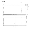
- collector layer 19, first layer 21, second layer 22, and third layer 23 are sequentially formed on silicon carbide single crystal substrate 18. This formation can be performed by, for example, CVD (Chemical Vapor Deposition). Silicon carbide single crystal substrate 18 has an n-type conductivity, for example. Next, silicon carbide single crystal substrate 18 is removed, for example, by back grinding (arrow GL in FIG. 4) (FIG. 5).
- a mask layer 60 having an opening is formed.
- the position of the opening corresponds to the position where the trench TR (FIG. 1) is to be formed.
- the material of mask layer 60 is, for example, silicon oxide.
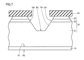
- etching is performed using the mask layer 60 as a mask. This etching is performed by, for example, thermal etching (details will be described later). By this etching, trench TR is formed (FIG. 7). Next, the mask layer 60 is removed.
- the channel layer 31 is formed on the sidewall SW and the bottom surface BS of the trench TR.
- a gate layer 32 sandwiching the channel layer 31 with the sidewall SW is formed.
- the channel layer 31 and the gate layer 32 can be formed by, for example, CVD.
- the channel layer 31 is exposed by patterning the gate layer 32.
- gate electrode 40 in contact with gate layer 32 is formed.
- an emitter electrode 41 that is separated from the gate layer 32 and is in contact with the channel layer 31 is formed.
- a collector electrode 42 is formed on the back surface P2 of the collector layer 19.
- thermal etching is performed by exposing an object to be etched to an etching gas at a high temperature, and has substantially no physical etching action.
- the thermal etching process gas preferably contains a halogen atom, and more preferably the halogen atom is a chlorine atom.
- the process gas may be Cl 2 gas.
- the process gas further includes a gas containing oxygen atoms in addition to the gas containing a halogen element.
- the gas containing oxygen atoms may be O 2 gas.
- the process gas may contain a carrier gas.
- the carrier gas for example, N 2 gas, Ar gas, or He gas can be used.
- the heat treatment temperature for thermal etching is preferably 700 ° C. or higher and 1200 ° C. or lower.
- the lower limit of this temperature is more preferably 800 ° C, and still more preferably 900 ° C.
- the upper limit of this temperature is more preferably 1100 ° C., still more preferably 1000 ° C.
- the etching rate can be set to a sufficiently practical value.
- the heat treatment temperature is set to 700 ° C. or higher and 1000 ° C. or lower, the etching rate of silicon carbide is about 70 ⁇ m / hr, for example.
- the etching for forming the trench TR is not limited to thermal etching, and other dry etching methods may be used.
- dry etching such as reactive ion etching or ion beam etching may be used.
- wet etching may be used instead of dry etching.
- the semiconductor device 90 of the present embodiment high-speed operation is possible by using the n-type switching element 80, that is, the unipolar element. Since the switching element 80 uses the junction gate 32 instead of the insulated gate, the channel mobility close to the theoretical channel mobility of SiC can be easily used. Thereby, the on-resistance of the switching element 80 can be easily reduced to a certain level.
- a p-type collector layer 19 is added to such an n-type switching element 80. That is, the switching element 80, which is a unipolar element, and the bipolar transistor are combined. As a result, a semiconductor device 90 capable of high-speed operation and having a low on-resistance and a high breakdown voltage can be obtained.
- the configuration of the switching element 80 used in the semiconductor device 90 is easy to manufacture.
- the conductivity type (second conductivity type) of the channel layer 31 of the switching element 80 is n-type. Thereby, the on-resistance of the switching element 80 can be reduced. Therefore, the on-resistance of the semiconductor device 90 can be further reduced.
- the trench TR has a tapered shape. Thereby, channel layer 31 can be easily formed on sidewall SW of trench TR.
- the semiconductor device 90 has an emitter electrode 41 connected to at least one of the third layer 23 and the channel layer 31 and separated from the gate layer 32. Thereby, carriers can be supplied from the emitter electrode 41 into the switching element 80.
- the semiconductor device 90V of the present embodiment has an emitter electrode 41V instead of the emitter electrode 41 of the first embodiment.
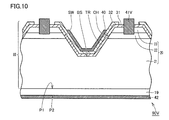
- the emitter electrode 41 ⁇ / b> V penetrates the third layer 23 and is connected to the second layer 22.
- the potential of the second layer 22 can be made to correspond to the potential of the emitter electrode 41V.
- the trench TR has a substantially flat bottom surface BS (FIGS. 1 and 10), but the configuration of the trench is not limited to this.
- a V-shaped trench that does not substantially have a bottom surface may be used.
- the trench TR has a mesh shape in which hexagonal shapes are combined (FIG. 3), the configuration of the trench is not limited to this.
- a mesh-like shape in which rectangular shapes (including squares) are combined may be used.
- the emitter electrode 41 is connected to the channel layer 31, but the configuration of the emitter electrode is not limited to this.
- the emitter electrode may be connected to the third layer 23.
- the emitter electrode and the channel layer 31 are electrically connected via the third layer 23.
- the trench TR has a tapered shape (FIG. 1)
- the configuration of the trench is not limited to this.
- the sidewall of the trench may be along the thickness direction (corresponding to the vertical direction in FIG. 1).
- the first conductivity type is p-type and the second conductivity type is n-type, but the first conductivity type is n-type and the second conductivity type is p-type. Also good.
Landscapes
- Bipolar Transistors (AREA)
- Junction Field-Effect Transistors (AREA)
- Electrodes Of Semiconductors (AREA)
Abstract
コレクタ層(19)は、第1の導電型を有する炭化珪素から作られている。スイッチング素子(80)はコレクタ層(19)上に設けられている。スイッチング素子(80)は、第1の導電型と異なる第2の導電型を有するチャネル(CH)を制御するための接合ゲート(32)を含む。
Description
この発明は炭化珪素半導体装置に関し、特に接合ゲートを有する炭化珪素半導体装置に関する。
電力用半導体装置として、たとえば、MOSFET(Metal Oxide Semiconductor Field Effect Transistor)、およびIGBT(Insulated Gate Bipolar Transistor:絶縁ゲートバイポーラトランジスタ)が広く用いられている(たとえば、非特許文献1:B. J. Baliga et al., “The insulated gate rectifier (IGR): A new power switching device,” IEDM Tech. Dig., 1982, pp. 264-267を参照)。IGBTはMOSFETとバイポーラトランジスタとが複合化された構成を有しており、これによりMOSFETと同様の高速動作と、バイポーラデバイスと同様の低いオン抵抗および高い耐圧とを有している。
電力用半導体装置の材料として、従来からシリコン(Si)が広く用いられている。Siに代わってより大きなバンドギャップを有する炭化珪素(SiC)を用いることで、オン抵抗などの性能が大幅に向上することが期待されている。
よって、MOSFETではなくIGBTを用い、かつ材料としてSiではなくSiCを用いれば、従来以上に、低いオン抵抗と高い耐圧とを有する電力用半導体装置が得られると期待される。しかしながらSiCを用いたIGBTは工業的には未だ実用化されていない。この一因は、SiCが用いられた場合、IGBTに含まれるMOS構造におけるチャネル移動度が理論値よりもはるかに小さく、この結果、オン抵抗が大きくなるためである。よってSiCが用いられたMOS構造におけるチャネル移動度を向上させる方法が検討されている(たとえば、特許文献1:特開2011-023675号を参照)。
B. J. Baliga et al., "The insulated gate rectifier (IGR): A new power switching device," IEDM Tech. Dig., 1982, pp. 264-267
しかしながら上記公報に記載の方法によっても、チャネル移動度を理論値に十分に近づけることは困難であると考えられる。よって、Siの代わりにSiCを用いかつMOSFETではなくIGBTを用いる場合に理論的に予想される低いオン抵抗と高い耐圧とは、依然として得られないと考えられる。
この発明は、上記のような課題を解決するために成されたものであり、この発明の目的は、高速動作が可能であり、かつ低いオン抵抗と高い耐圧とを有する炭化珪素半導体装置を提供することである。
本発明の炭化珪素半導体装置はコレクタ層およびスイッチング素子を有する。コレクタ層は、第1の導電型を有する炭化珪素から作られている。スイッチング素子はコレクタ層上に設けられている。スイッチング素子は、第1の導電型と異なる第2の導電型を有するチャネルを制御するための接合ゲートを含む。
この炭化珪素半導体装置によれば、第2の導電型のスイッチング素子、すなわちユニポーラ素子を含むことで、高速動作が可能である。またこのスイッチング素子は、絶縁ゲートではなく接合ゲートを用いるので、SiCの理論的なチャネル移動度に近いチャネル移動度を容易に利用し得る。これによりスイッチング素子のオン抵抗を容易に、ある程度まで小さくすることができる。このような、第2の導電型のスイッチング素子に対して、第1の導電型を有するコレクタ層が付加される。すなわち、ユニポーラ素子であるスイッチング素子とバイポーラトランジスタとが複合化される。これにより、高速動作が可能であり、かつ低いオン抵抗と高い耐圧とを有する炭化珪素半導体装置が得られる。
好ましくは第2の導電型はn型である。これにより、炭化珪素半導体装置のオン抵抗をより小さくすることができる。
好ましくはスイッチング素子は、半導体層と、チャネル層と、ゲート層と、ゲート電極とを含む。半導体層は、第1の層と、第2の層と、第3の層とを有する。第1の層は、コレクタ層上に設けられ、第2の導電型を有する。第2の層は、第1の層上に設けられ、第1の導電型を有する。第3の層は、第2の層上に設けられ、第2の導電型を有する。半導体層にはトレンチが設けられている。トレンチは、第3の層および第2の層を貫通して第1の層に至る側壁を有する。チャネル層は、トレンチの側壁上において第1~第3の層の各々に接し、第2の導電型を有する。ゲート層は、接合ゲートとしてのものであり、第2の層との間でチャネル層を挟み、第1の導電型を有する。ゲート電極はゲート層上に設けられている。これにより、スイッチング素子の構成を、製造が容易なものとすることができる。
好ましくはトレンチはテーパ状の形状を有する。これによりトレンチの側壁上へチャネル層を容易に形成し得る。
好ましくは、炭化珪素半導体装置は、第3の層およびチャネル層の少なくともいずれかに接続されゲート層から離されたエミッタ電極を有する。これによりエミッタ電極からスイッチング素子中へキャリアを供給することができる。
好ましくは、エミッタ電極は第2の層に接続されている。これにより第2の層の電位をエミッタ電極の電位に対応したものとすることができる。
上述したように本発明によれば、高速動作が可能であり、かつ低いオン抵抗と高い耐圧とを有する炭化珪素半導体装置が得られる。
以下、図面に基づいて本発明の実施の形態について説明する。なお、以下の図面において同一または相当する部分には同一の参照番号を付しその説明は繰返さない。
(実施の形態1)
図1~図3に示すように、本実施の形態の半導体装置90(炭化珪素半導体装置)は、コレクタ層19と、スイッチング素子80と、エミッタ電極41と、コレクタ電極42とを有する。コレクタ層19は、p型(第1の導電型)を有するSiCから作られており、好ましくは結晶構造として六方晶を有する。コレクタ層19は、上面P1と、上面P1と反対の面である裏面P2とを有する。
図1~図3に示すように、本実施の形態の半導体装置90(炭化珪素半導体装置)は、コレクタ層19と、スイッチング素子80と、エミッタ電極41と、コレクタ電極42とを有する。コレクタ層19は、p型(第1の導電型)を有するSiCから作られており、好ましくは結晶構造として六方晶を有する。コレクタ層19は、上面P1と、上面P1と反対の面である裏面P2とを有する。
スイッチング素子80はコレクタ層19の上面P1上に設けられている。スイッチング素子80は、n型(第1の導電型と異なる第2の導電型)を有するチャネルCHを制御するための接合ゲートを含む。すなわちスイッチング素子80は、ユニポーラ素子の一種であるJFET(Junction Field Effect Transistor)を含む。スイッチング素子80は、半導体層20と、チャネル層31と、ゲート層32(接合ゲート)と、ゲート電極40とを含む。
半導体層20はSiCから作られており、好ましくは結晶構造として六方晶を有する。半導体層20は、第1の層21と、第2の層22と、第3の層23とを有する。第1の層21は、コレクタ層19の上面P1上に設けられ、n型(第2の導電型)を有する。第2の層22は、第1の層21上に設けられ、p型(第1の導電型)を有する。第3の層23は、第2の層22上に設けられ、n型(第2の導電型)を有する。
半導体層20の上面(コレクタ層19がもうけられている面と反対の面)にはトレンチTRが設けられている。トレンチTRは側壁SWおよび底面BSを有する。側壁SWは、第3の層23および第2の層22を貫通して第1の層21に至る。好ましくは、トレンチTRはテーパ状の形状を有する。すなわち、上面P1に対するトレンチTRの側壁SWの傾きは0°よりも大きく直角よりも小さい。より好ましくは上面P1に対する側壁SWの傾きは10°以上である。
チャネル層31は、SiCから作られており、n型(第2の導電型)を有する。好ましくはチャネル層31は結晶構造として六方晶を有する。チャネル層31は、トレンチTRの側壁SW上において第1~第3の層21~23の各々に接している。チャネル層31は、図1に示すように、側壁SW上だけでなく、底面BS上にも設けられていてよい。側壁SW上におけるチャネル層31の厚さは、好ましくは50nm以上500nm以下である。
ゲート層32は、SiCから作られており、p型(第1の導電型)を有する。好ましくはゲート層32は結晶構造として六方晶を有する。ゲート層32は、接合ゲートとしてのものであり、第2の層22との間でチャネル層31を挟んでいる。ゲート電極40はゲート層32上に設けられている。
エミッタ電極41は、第3の層23およびチャネル層31の少なくともいずれかに接続され、かつゲート層32から離されている。図1においては、エミッタ電極41はチャネル層31に接続されている。エミッタ電極41はオーミック電極である。
コレクタ電極42は、コレクタ層19の裏面P2上に設けられている。コレクタ電極42はオーミック電極である。
次に半導体装置90の使用方法の例について説明する。半導体装置90は、エミッタ電極41およびコレクタ電極42の間の電気的導通を制御するスイッチング装置として用いられる。エミッタ電極41は負極側、コレクタ電極42は正極側として用いられる。半導体装置90は、スイッチング、すなわちオン/オフ動作の目的で制御されるチャネルCHを有するスイッチング素子80を含む。チャネルCHは、チャネル層31のうち、ゲート層32と、側壁SWのうち第2の層22からなる部分との間に挟まれた部分である。
チャネルCHへの電界印加によってチャネルCH中に空乏層が十分に形成されると、スイッチング素子80はオフ状態となる。そのためには、チャネルCH中のキャリアが十分に排斥されるような電位が、ゲート電極40を介してゲート層32に印加される。本実施の形態においては、絶対値が十分に大きい負の電位が印加される。逆にそのような電位が印加されていない場合は、チャネルCH中にキャリアが存在するので、スイッチング素子80はオン状態にある。なおオン状態の場合、第1の層21中において、n型(第2の導電型)のチャネルCHのキャリアである電子と、コレクタ層から注入された正孔との間で、対消滅が生じる。以上のように、ゲート電極40に印加される電位を変化させることで、スイッチング素子80がスイッチングされ、よって半導体装置90がスイッチングされる。
次に半導体装置90の製造方法について、以下に説明する。
図4に示すように、炭化珪素単結晶基板18上に、コレクタ層19、第1の層21、第2の層22、および第3の層23が順に形成される。この形成は、たとえばCVD(Chemical Vapor Deposition)により行われ得る。炭化珪素単結晶基板18の導電型は、たとえばn型である。次に炭化珪素単結晶基板18が、たとえばバックグラインド(図4の矢印GL)によって除去される(図5)。
図4に示すように、炭化珪素単結晶基板18上に、コレクタ層19、第1の層21、第2の層22、および第3の層23が順に形成される。この形成は、たとえばCVD(Chemical Vapor Deposition)により行われ得る。炭化珪素単結晶基板18の導電型は、たとえばn型である。次に炭化珪素単結晶基板18が、たとえばバックグラインド(図4の矢印GL)によって除去される(図5)。
図6に示すように、開口部を有するマスク層60が形成される。開口部の位置は、トレンチTR(図1)が形成されることになる位置に対応している。マスク層60の材料は、たとえば酸化珪素である。次にマスク層60をマスクとして用いたエッチングが行われる。このエッチングは、たとえば熱エッチング(詳しくは後述する)によって行われる。このエッチングによってトレンチTRが形成される(図7)。次にマスク層60が除去される。
図8に示すように、トレンチTRの側壁SWおよび底面BSの上に、チャネル層31が形成される。次にチャネル層31上での成膜が行われることで、側壁SWとの間でチャネル層31を挟むゲート層32が形成される。チャネル層31およびゲート層32は、たとえばCVDにより形成され得る。
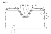
図9に示すように、ゲート層32がパターニングされることによって、チャネル層31が露出される。再び図1を参照して、ゲート層32に接触するゲート電極40が形成される。またゲート層32から離れ、チャネル層31に接触するエミッタ電極41が形成される。またコレクタ層19の裏面P2上にコレクタ電極42が形成される。以上により半導体装置90が得られる。
次に、上述した「熱エッチング」について説明する。熱エッチングとは、エッチングされる対象を高温下でエッチングガスにさらすことによって行われるものであり、物理的エッチング作用を実質的に有しないものである。熱エッチングを用いることによって、結晶学的に特定の側壁SWを自己形成することができる。熱エッチングのプロセスガスは、好ましくはハロゲン原子を含み、より好ましくはハロゲン原子は塩素原子である。具体的にはプロセスガスは、Cl2ガスであってもよい。好ましくは、プロセスガスは、ハロゲン元素を含有するガスに加えてさらに、酸素原子を含有するガスを含む。酸素原子を含有するガスは、具体的にはO2ガスであってもよい。なお、プロセスガスはキャリアガスを含んでいてもよい。キャリアガスとしては、たとえばN2ガス、Arガス、またはHeガスを用いることができる。熱エッチングの熱処理温度は、好ましくは700℃以上1200℃以下である。この温度の下限は、より好ましくは800℃、さらに好ましくは900℃である。またこの温度の上限は、より好ましくは1100℃、さらに好ましくは1000℃である。この場合、エッチング速度を十分実用的な値とすることができる。熱処理温度を700℃以上1000℃以下とした場合、炭化珪素のエッチング速度はたとえば70μm/hr程度になる。
なおトレンチTRを形成するためのエッチングは熱エッチングに限定されるものではなく、他のドライエッチング方法が用いられてもよい。たとえば、反応性イオンエッチングまたはイオンビームエッチングなどのドライエッチングが用いられてもよい。またドライエッチングの代わりにウエットエッチングが用いられてもよい。
本実施の形態の半導体装置90によれば、n型のスイッチング素子80、すなわちユニポーラ素子を用いることで、高速動作が可能とされる。またこのスイッチング素子80は、絶縁ゲートではなく接合ゲート32を用いるので、SiCの理論的なチャネル移動度に近いチャネル移動度を容易に利用し得る。これによりスイッチング素子80のオン抵抗を容易に、ある程度まで小さくすることができる。このような、n型のスイッチング素子80に対して、p型を有するコレクタ層19が付加される。すなわち、ユニポーラ素子であるスイッチング素子80とバイポーラトランジスタとが複合化される。これにより、高速動作が可能であり、かつ低いオン抵抗と高い耐圧とを有する半導体装置90が得られる。また半導体装置90に用いられるスイッチング素子80の構成は、製造が容易なものである。
またスイッチング素子80のチャネル層31の導電型(第2の導電型)はn型である。これによりスイッチング素子80のオン抵抗を小さくすることができる。よって半導体装置90のオン抵抗をより小さくすることができる。
またトレンチTRはテーパ状の形状を有する。これによりトレンチTRの側壁SW上へチャネル層31を容易に形成し得る。
また半導体装置90は、第3の層23およびチャネル層31の少なくともいずれかに接続されゲート層32から離されたエミッタ電極41を有する。これによりエミッタ電極41からスイッチング素子80中へキャリアを供給することができる。
(実施の形態2)
図10に示すように、本実施の形態の半導体装置90Vは、実施の形態1のエミッタ電極41の代わりにエミッタ電極41Vを有する。エミッタ電極41Vは第3の層23を貫通して第2の層22に接続されている。これにより第2の層22の電位をエミッタ電極41Vの電位に対応したものとすることができる。
図10に示すように、本実施の形態の半導体装置90Vは、実施の形態1のエミッタ電極41の代わりにエミッタ電極41Vを有する。エミッタ電極41Vは第3の層23を貫通して第2の層22に接続されている。これにより第2の層22の電位をエミッタ電極41Vの電位に対応したものとすることができる。
なお上記各実施の形態においてはトレンチTRがほぼ平坦な底面BSを有するが(図1および図10)、トレンチの構成はこのようなものに限定されるものではない。たとえば、実質的に底面が設けられないような、V字状のトレンチが用いられてもよい。
またトレンチTRは、六角形の形状が組み合わされた網目状の形状を有するが(図3)、トレンチの構成はこのようなものに限定されるものではない。たとえば、長方形(正方形を含む)の形状が組み合わされた網の目状の形状が用いられてもよい。
また図1においてはエミッタ電極41はチャネル層31に接続されているが、エミッタ電極の構成はこのようなものに限定されるものではない。たとえば、エミッタ電極が第3の層23に接続されてもよい。この場合、第3の層23を介してエミッタ電極とチャネル層31とが電気的に接続される。
またトレンチTRはテーパ状の形状を有するが(図1)、トレンチの構成はこのようなものに限定されるものではない。たとえば、トレンチの側壁は、厚さ方向(図1の縦方向に対応)に沿っていてもよい。
また上記説明においては第1の導電型がp型でありかつ第2の導電型がn型であるが、第1の導電型がn型でありかつ第2の導電型がp型であってもよい。
今回開示された実施の形態はすべての点で例示であって制限的なものではないと考えられるべきである。本発明の範囲は上記した実施の形態ではなくて請求の範囲によって示され、請求の範囲と均等の意味および範囲内でのすべての変更が含まれることが意図される。
18 炭化珪素単結晶基板、19 コレクタ層、20 半導体層、21 第1の層、22 第2の層、23 第3の層、31 チャネル層、32 ゲート層、40 ゲート電極、41,41V エミッタ電極、42 コレクタ電極、90,90V 半導体装置(炭化珪素半導体装置)、SW 側壁、TR トレンチ。
Claims (6)
- 第1の導電型を有する炭化珪素から作られたコレクタ層と、
前記コレクタ層上に設けられたスイッチング素子とを備え、前記スイッチング素子は、前記第1の導電型と異なる第2の導電型を有するチャネルを制御するための接合ゲートを含む、炭化珪素半導体装置。 - 前記第2の導電型はn型である、請求項1に記載の炭化珪素半導体装置。
- 前記スイッチング素子は、
前記コレクタ層上に設けられ前記第2の導電型を有する第1の層と、前記第1の層上に設けられ前記第1の導電型を有する第2の層と、前記第2の層上に設けられ前記第2の導電型を有する第3の層とを有する半導体層を含み、前記半導体層には、前記第1の層および前記第2の層を貫通して前記第3の層に至る側壁を有するトレンチが設けられており、前記スイッチング素子はさらに
前記トレンチの前記側壁上において前記第1~第3の層の各々に接し、前記第2の導電型を有するチャネル層と、
前記第2の層との間で前記チャネル層を挟み、前記第1の導電型を有する、前記接合ゲートとしてのゲート層と、
前記ゲート層上に設けられたゲート電極とを含む、請求項1または2に記載の炭化珪素半導体装置。 - 前記トレンチはテーパ状の形状を有する、請求項3に記載の炭化珪素半導体装置。
- 前記第3の層および前記チャネル層の少なくともいずれかに接続され、前記ゲート層から離されたエミッタ電極をさらに備える、請求項3または4に記載の炭化珪素半導体装置。
- 前記エミッタ電極は前記第2の層に接続されている、請求項5に記載の炭化珪素半導体装置。
Priority Applications (2)
| Application Number | Priority Date | Filing Date | Title |
|---|---|---|---|
| CN201380026182.3A CN104321855B (zh) | 2012-06-26 | 2013-04-23 | 碳化硅半导体器件 |
| EP13809313.3A EP2866251A4 (en) | 2012-06-26 | 2013-04-23 | SEMICONDUCTOR ELEMENT FROM SILICON CARBIDE |
Applications Claiming Priority (2)
| Application Number | Priority Date | Filing Date | Title |
|---|---|---|---|
| JP2012-142830 | 2012-06-26 | ||
| JP2012142830A JP5880311B2 (ja) | 2012-06-26 | 2012-06-26 | 炭化珪素半導体装置 |
Publications (1)
| Publication Number | Publication Date |
|---|---|
| WO2014002597A1 true WO2014002597A1 (ja) | 2014-01-03 |
Family
ID=49773664
Family Applications (1)
| Application Number | Title | Priority Date | Filing Date |
|---|---|---|---|
| PCT/JP2013/061919 Ceased WO2014002597A1 (ja) | 2012-06-26 | 2013-04-23 | 炭化珪素半導体装置 |
Country Status (5)
| Country | Link |
|---|---|
| US (1) | US8866155B2 (ja) |
| EP (1) | EP2866251A4 (ja) |
| JP (1) | JP5880311B2 (ja) |
| CN (1) | CN104321855B (ja) |
| WO (1) | WO2014002597A1 (ja) |
Families Citing this family (5)
| Publication number | Priority date | Publication date | Assignee | Title |
|---|---|---|---|---|
| JP6199755B2 (ja) * | 2014-01-27 | 2017-09-20 | トヨタ自動車株式会社 | 半導体装置 |
| WO2017138398A1 (ja) * | 2016-02-08 | 2017-08-17 | パナソニック株式会社 | 半導体装置 |
| CN108735795B (zh) * | 2017-04-21 | 2021-09-03 | 苏州能屋电子科技有限公司 | (0001)面外延的六方相SiC晶圆、UMOSFET器件及其制作方法 |
| US11621328B2 (en) | 2017-11-16 | 2023-04-04 | Panasonic Holdings Corporation | Nitride semiconductor device |
| US10276667B1 (en) | 2018-05-31 | 2019-04-30 | Silanna Asia Pte Ltd | High voltage breakdown tapered vertical conduction junction transistor |
Citations (4)
| Publication number | Priority date | Publication date | Assignee | Title |
|---|---|---|---|---|
| JPH0730111A (ja) * | 1993-07-15 | 1995-01-31 | Hitachi Ltd | 絶縁ゲート形電界効果トランジスタ |
| JP2002359378A (ja) * | 2001-03-28 | 2002-12-13 | Toshiba Corp | 半導体装置及びその製造方法 |
| JP2003069038A (ja) * | 2001-08-29 | 2003-03-07 | Denso Corp | 炭化珪素半導体装置およびその製造方法 |
| JP2011023675A (ja) | 2009-07-21 | 2011-02-03 | Hitachi Ltd | 半導体装置及びその製造方法 |
Family Cites Families (13)
| Publication number | Priority date | Publication date | Assignee | Title |
|---|---|---|---|---|
| US5359220A (en) * | 1992-12-22 | 1994-10-25 | Hughes Aircraft Company | Hybrid bipolar/field-effect power transistor in group III-V material system |
| US5753938A (en) * | 1996-08-08 | 1998-05-19 | North Carolina State University | Static-induction transistors having heterojunction gates and methods of forming same |
| JP2000312008A (ja) * | 1999-04-27 | 2000-11-07 | Fuji Electric Co Ltd | 炭化珪素静電誘導トランジスタおよびその製造方法 |
| JP2002305304A (ja) * | 2001-04-05 | 2002-10-18 | Toshiba Corp | 電力用半導体装置 |
| JP3994703B2 (ja) * | 2001-08-29 | 2007-10-24 | 株式会社デンソー | 炭化珪素半導体装置およびその製造方法 |
| US7217950B2 (en) * | 2002-10-11 | 2007-05-15 | Nissan Motor Co., Ltd. | Insulated gate tunnel-injection device having heterojunction and method for manufacturing the same |
| JP4179139B2 (ja) * | 2003-11-14 | 2008-11-12 | 株式会社デンソー | 炭化珪素半導体装置およびその製造方法 |
| JP5051980B2 (ja) * | 2005-03-31 | 2012-10-17 | 住友電工デバイス・イノベーション株式会社 | 半導体装置 |
| JP2008226997A (ja) * | 2007-03-09 | 2008-09-25 | Sumitomo Electric Ind Ltd | 半導体装置およびその製造方法 |
| JP4888341B2 (ja) * | 2007-10-31 | 2012-02-29 | 株式会社デンソー | 炭化珪素半導体装置 |
| JP5061998B2 (ja) * | 2008-03-28 | 2012-10-31 | 株式会社デンソー | スイッチング回路 |
| JP5638067B2 (ja) * | 2010-04-15 | 2014-12-10 | 良孝 菅原 | 半導体装置 |
| US20130240900A1 (en) * | 2010-11-04 | 2013-09-19 | Sumitomo Electric Industries, Ltd. | Semiconductor device and method for producing the same |
-
2012
- 2012-06-26 JP JP2012142830A patent/JP5880311B2/ja not_active Expired - Fee Related
-
2013
- 2013-04-23 WO PCT/JP2013/061919 patent/WO2014002597A1/ja not_active Ceased
- 2013-04-23 CN CN201380026182.3A patent/CN104321855B/zh not_active Expired - Fee Related
- 2013-04-23 EP EP13809313.3A patent/EP2866251A4/en not_active Withdrawn
- 2013-05-15 US US13/895,036 patent/US8866155B2/en not_active Expired - Fee Related
Patent Citations (4)
| Publication number | Priority date | Publication date | Assignee | Title |
|---|---|---|---|---|
| JPH0730111A (ja) * | 1993-07-15 | 1995-01-31 | Hitachi Ltd | 絶縁ゲート形電界効果トランジスタ |
| JP2002359378A (ja) * | 2001-03-28 | 2002-12-13 | Toshiba Corp | 半導体装置及びその製造方法 |
| JP2003069038A (ja) * | 2001-08-29 | 2003-03-07 | Denso Corp | 炭化珪素半導体装置およびその製造方法 |
| JP2011023675A (ja) | 2009-07-21 | 2011-02-03 | Hitachi Ltd | 半導体装置及びその製造方法 |
Non-Patent Citations (2)
| Title |
|---|
| B. J. BALIGA ET AL.: "The insulated gate rectifier (IGR): A new power switching device", IEDM TECH. DIG., 1982, pages 264 - 267 |
| See also references of EP2866251A4 |
Also Published As
| Publication number | Publication date |
|---|---|
| CN104321855A (zh) | 2015-01-28 |
| US8866155B2 (en) | 2014-10-21 |
| JP5880311B2 (ja) | 2016-03-09 |
| JP2014007326A (ja) | 2014-01-16 |
| EP2866251A4 (en) | 2016-03-02 |
| CN104321855B (zh) | 2017-04-12 |
| US20130341645A1 (en) | 2013-12-26 |
| EP2866251A1 (en) | 2015-04-29 |
Similar Documents
| Publication | Publication Date | Title |
|---|---|---|
| US8354715B2 (en) | Semiconductor device and method of fabricating the same | |
| JP2014107420A (ja) | 炭化珪素半導体装置およびその製造方法 | |
| JP6705155B2 (ja) | 半導体装置および半導体装置の製造方法 | |
| JP6766512B2 (ja) | 半導体装置および半導体装置の製造方法 | |
| JP6802454B2 (ja) | 半導体装置およびその製造方法 | |
| JP2012243966A (ja) | 半導体装置 | |
| TWI534910B (zh) | 半導體裝置的製造方法 | |
| JP2015026727A (ja) | 炭化珪素半導体装置およびその製造方法 | |
| WO2010098076A1 (ja) | 蓄積型絶縁ゲート型電界効果型トランジスタ | |
| JP6853977B2 (ja) | 半導体装置および半導体装置の製造方法 | |
| JP2015056644A (ja) | 炭化珪素半導体装置および炭化珪素半導体装置の製造方法 | |
| WO2015015926A1 (ja) | 炭化珪素半導体装置およびその製造方法 | |
| JP2018206872A (ja) | 半導体装置 | |
| JP5880311B2 (ja) | 炭化珪素半導体装置 | |
| JP5233158B2 (ja) | 炭化珪素半導体装置 | |
| CN103367405A (zh) | 半导体装置及其制造方法 | |
| JP6862782B2 (ja) | 半導体装置および半導体装置の製造方法 | |
| WO2015015938A1 (ja) | 炭化珪素半導体装置の製造方法 | |
| JP2019029501A (ja) | 半導体装置および半導体装置の製造方法 | |
| JP5867134B2 (ja) | 炭化珪素半導体装置の製造方法 | |
| JP2017092364A (ja) | 半導体装置および半導体装置の製造方法 | |
| WO2018135146A1 (ja) | 半導体装置および半導体装置の製造方法 | |
| CN109219869B (zh) | 半导体装置 | |
| JP6029330B2 (ja) | 半導体装置およびその製造方法 | |
| JP2021010027A (ja) | 半導体装置および半導体装置の製造方法 |
Legal Events
| Date | Code | Title | Description |
|---|---|---|---|
| 121 | Ep: the epo has been informed by wipo that ep was designated in this application |
Ref document number: 13809313 Country of ref document: EP Kind code of ref document: A1 |
|
| WWE | Wipo information: entry into national phase |
Ref document number: 2013809313 Country of ref document: EP |
|
| NENP | Non-entry into the national phase |
Ref country code: DE |