WO2014007327A1 - 回路基板用積層板、金属ベース回路基板及びパワーモジュール - Google Patents
回路基板用積層板、金属ベース回路基板及びパワーモジュール Download PDFInfo
- Publication number
- WO2014007327A1 WO2014007327A1 PCT/JP2013/068361 JP2013068361W WO2014007327A1 WO 2014007327 A1 WO2014007327 A1 WO 2014007327A1 JP 2013068361 W JP2013068361 W JP 2013068361W WO 2014007327 A1 WO2014007327 A1 WO 2014007327A1
- Authority
- WO
- WIPO (PCT)
- Prior art keywords
- circuit board
- cyanate resin
- laminate
- insulating layer
- metal
- Prior art date
- Legal status (The legal status is an assumption and is not a legal conclusion. Google has not performed a legal analysis and makes no representation as to the accuracy of the status listed.)
- Ceased
Links
Images


Classifications
-
- B—PERFORMING OPERATIONS; TRANSPORTING
- B32—LAYERED PRODUCTS
- B32B—LAYERED PRODUCTS, i.e. PRODUCTS BUILT-UP OF STRATA OF FLAT OR NON-FLAT, e.g. CELLULAR OR HONEYCOMB, FORM
- B32B15/00—Layered products comprising a layer of metal
- B32B15/04—Layered products comprising a layer of metal comprising metal as the main or only constituent of a layer, which is next to another layer of the same or of a different material
- B32B15/08—Layered products comprising a layer of metal comprising metal as the main or only constituent of a layer, which is next to another layer of the same or of a different material of synthetic resin
-
- H—ELECTRICITY
- H05—ELECTRIC TECHNIQUES NOT OTHERWISE PROVIDED FOR
- H05K—PRINTED CIRCUITS; CASINGS OR CONSTRUCTIONAL DETAILS OF ELECTRIC APPARATUS; MANUFACTURE OF ASSEMBLAGES OF ELECTRICAL COMPONENTS
- H05K1/00—Printed circuits
- H05K1/02—Details
- H05K1/03—Use of materials for the substrate
- H05K1/05—Insulated conductive substrates, e.g. insulated metal substrate
- H05K1/056—Insulated conductive substrates, e.g. insulated metal substrate the metal substrate being covered by an organic insulating layer
-
- H—ELECTRICITY
- H10—SEMICONDUCTOR DEVICES; ELECTRIC SOLID-STATE DEVICES NOT OTHERWISE PROVIDED FOR
- H10W—GENERIC PACKAGES, INTERCONNECTIONS, CONNECTORS OR OTHER CONSTRUCTIONAL DETAILS OF DEVICES COVERED BY CLASS H10
- H10W40/00—Arrangements for thermal protection or thermal control
- H10W40/20—Arrangements for cooling
- H10W40/25—Arrangements for cooling characterised by their materials
- H10W40/255—Arrangements for cooling characterised by their materials having a laminate or multilayered structure, e.g. direct bond copper [DBC] ceramic substrates
-
- H—ELECTRICITY
- H10—SEMICONDUCTOR DEVICES; ELECTRIC SOLID-STATE DEVICES NOT OTHERWISE PROVIDED FOR
- H10W—GENERIC PACKAGES, INTERCONNECTIONS, CONNECTORS OR OTHER CONSTRUCTIONAL DETAILS OF DEVICES COVERED BY CLASS H10
- H10W70/00—Package substrates; Interposers; Redistribution layers [RDL]
- H10W70/60—Insulating or insulated package substrates; Interposers; Redistribution layers
- H10W70/67—Insulating or insulated package substrates; Interposers; Redistribution layers characterised by their insulating layers or insulating parts
- H10W70/68—Shapes or dispositions thereof
- H10W70/6875—Shapes or dispositions thereof being on a metallic substrate, e.g. insulated metal substrates [IMS]
-
- H—ELECTRICITY
- H10—SEMICONDUCTOR DEVICES; ELECTRIC SOLID-STATE DEVICES NOT OTHERWISE PROVIDED FOR
- H10W—GENERIC PACKAGES, INTERCONNECTIONS, CONNECTORS OR OTHER CONSTRUCTIONAL DETAILS OF DEVICES COVERED BY CLASS H10
- H10W70/00—Package substrates; Interposers; Redistribution layers [RDL]
- H10W70/60—Insulating or insulated package substrates; Interposers; Redistribution layers
- H10W70/67—Insulating or insulated package substrates; Interposers; Redistribution layers characterised by their insulating layers or insulating parts
- H10W70/69—Insulating materials thereof
-
- H—ELECTRICITY
- H05—ELECTRIC TECHNIQUES NOT OTHERWISE PROVIDED FOR
- H05K—PRINTED CIRCUITS; CASINGS OR CONSTRUCTIONAL DETAILS OF ELECTRIC APPARATUS; MANUFACTURE OF ASSEMBLAGES OF ELECTRICAL COMPONENTS
- H05K1/00—Printed circuits
- H05K1/02—Details
- H05K1/03—Use of materials for the substrate
- H05K1/0313—Organic insulating material
- H05K1/0353—Organic insulating material consisting of two or more materials, e.g. two or more polymers, polymer + filler, + reinforcement
- H05K1/0373—Organic insulating material consisting of two or more materials, e.g. two or more polymers, polymer + filler, + reinforcement containing additives, e.g. fillers
-
- H—ELECTRICITY
- H05—ELECTRIC TECHNIQUES NOT OTHERWISE PROVIDED FOR
- H05K—PRINTED CIRCUITS; CASINGS OR CONSTRUCTIONAL DETAILS OF ELECTRIC APPARATUS; MANUFACTURE OF ASSEMBLAGES OF ELECTRICAL COMPONENTS
- H05K2201/00—Indexing scheme relating to printed circuits covered by H05K1/00
- H05K2201/02—Fillers; Particles; Fibers; Reinforcement materials
- H05K2201/0203—Fillers and particles
- H05K2201/0206—Materials
- H05K2201/0209—Inorganic, non-metallic particles
-
- H—ELECTRICITY
- H10—SEMICONDUCTOR DEVICES; ELECTRIC SOLID-STATE DEVICES NOT OTHERWISE PROVIDED FOR
- H10W—GENERIC PACKAGES, INTERCONNECTIONS, CONNECTORS OR OTHER CONSTRUCTIONAL DETAILS OF DEVICES COVERED BY CLASS H10
- H10W90/00—Package configurations
- H10W90/701—Package configurations characterised by the relative positions of pads or connectors relative to package parts
- H10W90/731—Package configurations characterised by the relative positions of pads or connectors relative to package parts of die-attach connectors
- H10W90/734—Package configurations characterised by the relative positions of pads or connectors relative to package parts of die-attach connectors between a chip and a stacked insulating package substrate, interposer or RDL
-
- Y—GENERAL TAGGING OF NEW TECHNOLOGICAL DEVELOPMENTS; GENERAL TAGGING OF CROSS-SECTIONAL TECHNOLOGIES SPANNING OVER SEVERAL SECTIONS OF THE IPC; TECHNICAL SUBJECTS COVERED BY FORMER USPC CROSS-REFERENCE ART COLLECTIONS [XRACs] AND DIGESTS
- Y10—TECHNICAL SUBJECTS COVERED BY FORMER USPC
- Y10T—TECHNICAL SUBJECTS COVERED BY FORMER US CLASSIFICATION
- Y10T428/00—Stock material or miscellaneous articles
- Y10T428/31504—Composite [nonstructural laminate]
- Y10T428/31678—Of metal
Definitions
- the present invention relates to a laminate for a circuit board, a metal-based circuit board manufactured from the laminate for the circuit board, and a power module including the metal-based circuit board.
- Patent Documents 1 to 4 disclose a thermally conductive substrate provided with a high heat resistant prepreg in which a substrate is impregnated with a cyanate resin-containing composition, and a heat transfer sheet layer made of a cured product of the cyanate resin-containing composition. It is done.
- Patent Document 5 discloses a multilayer printed wiring board provided with a cyanate resin-containing insulating sheet capable of maintaining a high elastic modulus even at high temperatures.
- the metal base circuit board has a structure in which an insulating layer and a circuit pattern are laminated in this order on at least one surface of the metal board. It is a metal base circuit board which is excellent in heat resistance, durability, solder connection reliability, and has long-term reliability even when using a known cyanate resin-containing composition as described above as a resin composition for forming the insulating layer. The fact is that manufacturing is difficult.
- a laminated board for a circuit board comprising a metal substrate, an insulating layer provided on at least one side of the metal substrate, and a metal foil provided on the insulating layer
- the present invention provides a laminate for a circuit board, wherein the insulating layer contains a crosslinkable copolymer of a bisphenol cyanate resin and a novolac cyanate resin and an inorganic filler.
- the mass ratio of the bisphenol-type cyanate resin to the novolac-type cyanate resin contained in the insulating layer is, for example, 3: 1 to 1:11.
- the insulating layer contains, for example, at least one selected from alumina, surface-treated alumina, aluminum nitride, and boron nitride as an inorganic filler.
- the insulating layer further contains a curing accelerator.
- the curing accelerator is, for example, a borate complex, and the borate complex may be a phosphorus-based borate complex or a non-phosphorus-based borate complex.
- the insulating layer contains a phosphorus-based borate complex as a curing accelerator, and contains at least one selected from surface-treated alumina, aluminum nitride and boron nitride as an inorganic filler. And more preferably contains two or more.
- the insulating layer contains a non-phosphorus borate complex as a curing accelerator, and is at least one selected from alumina, a surface-treated alumina, aluminum nitride and boron nitride as an inorganic filler. It contains one kind, more preferably contains two or more kinds.
- a metal-based circuit board obtained by patterning the metal foil of the above-mentioned laminate for circuit board.
- a power module comprising the metal-based circuit board.
- the present invention it has become possible to provide a metal-based circuit board which is excellent in heat resistance, durability and solder connection reliability and has long-term reliability.
- the present invention also makes it possible to provide a power module comprising this metal-based circuit board.
- FIG. 1 is a cross-sectional view schematically showing a power module according to an aspect of the present invention. Sectional drawing which shows the conventional power module roughly.
- the laminate 1 for a circuit board shown in FIGS. 1 and 2 has a three-layer structure in which an insulating layer 3 is formed on one side of a metal substrate 2 and a metal foil 4 is formed on the insulating layer 3.
- the insulating layer 3 may be formed on both sides of the metal plate 2, and the metal foil 4 may be further formed on each insulating layer 3.
- the X and Y directions are directions parallel to the main surface of the metal substrate 2 and orthogonal to each other, and the Z direction is a thickness direction perpendicular to the X and Y directions.
- the rectangular circuit board laminate 1 is shown as an example, but the circuit board laminate 1 may have another shape.
- the insulating layer contains a bisphenol-type cyanate resin, a novolac-type cyanate resin, and an inorganic filler, and it is the first matter that the bisphenol-type cyanate resin and the novolac-type cyanate resin form a cross-linked copolymer.
- the glass transition temperature (Tg) and mechanical properties of the cured product differ depending on the type of molecular structure, even if it is the same cyanate resin that is characterized, for example, it is simply high to improve the heat resistance and toughness of the insulating layer
- the desired high heat resistance and toughness can not be obtained only by using the heat resistant resin and the toughness resin in combination.
- the performance (hereinafter also referred to as the “heat cycle performance”) of indirectly relieving the stress on the solder connection due to the heat cycle in the insulating layer is enhanced, and thus the solder It becomes possible to improve connection reliability.
- a curing reaction (cyclization / trimerization reaction) tends to proceed during melting due to melting point depression, and as a result, almost no unreacted group remains, so long-term reliability (eg, long-term reliability) And solder connection reliability) can be improved.
- the mixed system of bisphenol type cyanate resin and novolac type cyanate resin has low elasticity, which also enhances the heat cycle performance of the insulating layer and contributes to the improvement of solder connection reliability.
- bisphenol type cyanate resin used by this invention bisphenol A type cyanate resin, bisphenol E type phenol resin, tetramethyl bisphenol F type cyanate resin etc. can be mentioned, for example.
- the weight average molecular weight of the bisphenol type cyanate resin is not particularly limited, and may be an oligomer or a monomer.
- bisphenol type cyanate resin used in the present invention for example, from the viewpoint of heat resistance, tetramethyl bisphenol F type cyanate resin, bisphenol A type cyanate resin, and bisphenol E type cyanate resin are superior in this order, and from the viewpoint of reactivity Bisphenol A type cyanate resin is excellent.
- novolac cyanate resins used in the present invention include phenol novolac cyanate resins and cresol novolac cyanate resins.
- the weight average molecular weight of the novolac cyanate resin is not particularly limited, and may be an oligomer or a monomer.
- a phenol novolak type cyanate resin is excellent, for example from a reactive viewpoint.
- the mass ratio of the bisphenol-type cyanate resin to the novolac-type cyanate resin contained in the insulating layer of the present invention is, for example, preferably 3: 1 to 1:11, more preferably 3: 1 to 1: 3, and 2.5 1 to 1: 2 is more preferable. If the compounding ratio of the bisphenol-type cyanate resin is too large, the glass transition temperature (Tg) may be low and desired heat resistance may not be obtained. On the other hand, when the compounding ratio of the novolak type cyanate resin is too large, the toughness is lowered, and it is not preferable from the viewpoint of reactivity.
- the insulating layer contains an inorganic filler together with a bisphenol-type cyanate resin and a novolac-type cyanate resin.
- the inorganic filler include alumina, aluminum nitride, boron nitride, silicon nitride, magnesium oxide, silicon oxide and the like, and it is preferable to use one or more selected from these.
- a bisphenol type cyanate resin and a novolac type cyanate resin are cross-linked copolymers
- problems which do not occur in a system using a single resin may occur. Specifically, the reaction heat is absorbed by the inorganic filler, so that the curing reaction may be delayed, or the surface functional group of the inorganic filler may inhibit the curing reaction of the cyanate group.
- a surface-treated inorganic filler may be used, and it is preferable to use an inorganic filler in an appropriate combination with the effect promoter described later.
- the surface of the inorganic filler may be modified with a functional group capable of chemically bonding with the cyanate resin, or modified with a functional group having high compatibility with the cyanate resin.
- cyanate group, epoxy group, amino group, hydroxyl group, carboxyl group, vinyl group, styryl group, methacryl group, acrylic group, ureido group, mercapto group, sulfide group, isocyanate group, etc. eg, silane cup Ring processing, plasma processing, etc.
- the proportion of the inorganic filler contained in the insulating layer of the present invention is preferably 50 to 90% by volume based on the total volume of the novolac cyanate resin and the bisphenol cyanate resin.
- the content of the inorganic filler is more preferably 60 to 80% by volume.
- the insulating layer may contain a curing accelerator.
- the curing accelerator is not particularly limited, and examples thereof include borate complexes.
- the borate complex may be a phosphorus-based borate complex or a non-phosphorus-based borate complex.
- Examples of phosphorus-based borate complexes include tetraphenylphosphonium tetraphenylborate, tetraphenylphosphonium tetra-p-tolylborate, tri-tert-butylphosphonium tetraphenylborate, di-tert-butylmethylphosphonium tetraphenylborate, and p-tolyltriolate. Phenylphosphonium tetra-p-tolylborate, tetraphenylphosphonium tetrafluoroborate, triphenylphosphine triphenylborate and the like can be mentioned.
- non-phosphorus borate complexes examples include sodium tetraphenylborate, pyridinetriphenylborate, 2-ethyl-4-methylimidazolium tetraphenylborate, 1,5-diazobicyclo [4.3.0] nonene-5- Tetraphenyl borate, lithium triphenyl (n-butyl) borate and the like can be mentioned.
- the insulating layer contains a phosphorus-based borate complex as a curing accelerator, and contains at least one selected from surface-treated alumina, aluminum nitride and boron nitride as an inorganic filler. It is preferable to contain a phosphorus-based borate complex and at least two or more selected from surface-treated alumina, aluminum nitride and boron nitride. In particular, it is preferable to use surface-treated alumina in combination with a phosphorus-based borate complex which is a curing accelerator because alumina inhibits the curing reaction of cyanate resin (for example, adverse effect due to steric hindrance of molecular structure) . Curing inhibition can be prevented by modifying the surface of the particles in advance.
- the insulating layer contains a non-phosphorus borate complex as a curing accelerator, and is selected from alumina, alumina, aluminum nitride and boron nitride surface-treated as an inorganic filler. It is preferable to contain at least one kind, and it is more preferable to contain at least two kinds selected from non-phosphorus borate complexes and surface-treated alumina, alumina, aluminum nitride and boron nitride.
- non-phosphorus borate complex When a non-phosphorus borate complex is used as a curing accelerator, a combination with alumina which is not subjected to surface treatment can be suitably used as compared with the case where a phosphorus-based borate complex is used.
- non-phosphorus borate complex has higher activity as a hardening accelerator in the system where aluminum oxide exists compared to phosphorus borate complex, and aluminum oxide uses non-phosphorus borate complex It is presumed that the small adverse effect (e.g., steric hindrance of molecular structure) exerted on the curing accelerating system is a cause.
- a curing accelerator When a curing accelerator is added to the insulating layer of the present invention, its content is preferably 0.1 to 5% by mass based on the total mass of novolac cyanate resin and bisphenol cyanate resin, and more preferably It is 0.5 to 2% by mass.
- the insulating layer is a coating film formed of a resin composition (hereinafter, also referred to as “the composition of the present invention” or the like) in which a component containing the above-mentioned bisphenol cyanate resin, novolac cyanate resin and inorganic filler is dissolved in a solvent.
- a resin composition hereinafter, also referred to as “the composition of the present invention” or the like
- Is a cured product of As the solvent for example, N-methylpyrrolidone, dimethylacetamide, tetrafluoroisopropanol, methyl ethyl ketone, ethylene diglycol acetate, propylene glycol monomethyl ether acetate, methyl isobutyl ketone, ethylene glycol monomethyl ether, tetrahydrofuran, chloroform, toluene, xylene, acetone,
- the solvent for example, N-methylpyrrolidone, dimethylacetamide, tetrafluoroisopropanol, methyl ethyl ketone, ethylene diglycol acetate, propylene glycol monomethyl ether acetate, methyl isobutyl ketone, ethylene glycol monomethyl ether, tetrahydrofuran, chloroform, toluene, xylene, acetone
- Examples include dioxane, dimethyl sulfox
- the solid concentration is, for example, preferably 1 to 50% by mass, and more preferably 15 to 35% by mass.
- the amount of solvent is excessively large, a large amount of solvent must be removed from the coating, which tends to cause appearance defects of the coating. In addition, productivity is reduced because a large amount of drying time is required.
- the amount of the solvent is excessively small, the composition tends to have high viscosity, and the handleability thereof is lowered.
- composition of the present invention may contain various additives in addition to the above-mentioned bisphenol-type cyanate resin, novolac-type cyanate resin, inorganic filler and curing accelerator, for example, a silane coupling agent and titanium coupling Coupling agents, ion adsorbents, anti-settling agents, hydrolysis inhibitors, leveling agents, antioxidants and the like.
- additives for example, a silane coupling agent and titanium coupling Coupling agents, ion adsorbents, anti-settling agents, hydrolysis inhibitors, leveling agents, antioxidants and the like.
- the metal substrate 2 is made of, for example, a single metal or an alloy. As a material of the metal substrate 2, for example, aluminum, iron, copper, an aluminum alloy, or stainless steel can be used.
- the metal substrate 2 may further contain a nonmetal such as carbon.
- the metal substrate 2 may contain aluminum complexed with carbon.
- the metal substrate 2 may have a single-layer structure or a multi-layer structure.
- the metal substrate 2 has high thermal conductivity. Typically, the metal substrate 2 has a thermal conductivity of 60 W ⁇ m ⁇ 1 ⁇ K ⁇ 1 or more.
- the metal substrate 2 may have flexibility or may not have flexibility.
- the thickness of the metal substrate 2 is, for example, in the range of 0.2-5 mm.
- the metal foil 4 is provided on the insulating layer 3.
- the metal foil 4 faces the metal substrate 2 with the insulating layer 3 interposed therebetween.
- the metal foil 4 is made of, for example, a single metal or an alloy.
- the thickness of the metal foil 4 is, for example, in the range of 10 to 500 ⁇ m.
- the circuit board laminate 1 is manufactured, for example, by the following method. First, the above-mentioned bisphenol-type cyanate resin and novolac-type cyanate resin and a curing accelerator are mixed by heating, and then dissolved in a solvent to obtain a solution. Next, the above-mentioned inorganic filler is dispersed in a solution to obtain a dispersion.
- the inorganic filler may be dispersed in the above solution while being ground using, for example, a ball mill, a triple roll, a centrifugal stirrer or a bead mill. Further, prior to adding the inorganic filler to the solution, additives such as a silane coupling agent and an ion adsorbent may be added to the solution.
- this dispersion is applied to at least one of the metal substrate 2 and the metal foil 4.
- the dispersion for example, roll coating, bar coating or screen printing can be used. It may be carried out in a continuous manner or in a single plate manner.
- the laminated board 1 for circuit boards is obtained as mentioned above.
- a coating is formed by applying the dispersion, which is the composition of the present invention, to at least one of the metal plate 2 and the metal foil 4, but in another embodiment, the dispersion is used as a substrate such as a PET film
- a coating film may be formed in advance by coating and drying, and this may be thermally transferred to one of the metal substrate 2 and the metal foil 4.
- a metal base circuit board 1 'obtained from the above-described circuit board laminate 1 will be described.
- a metal base circuit board 1 'shown in FIG. 3 is obtained from the laminate for circuit board shown in FIGS. 1 and 2, and includes a metal board 2, an insulating layer 3, and a circuit pattern 4'. .
- the circuit pattern 4 ′ is obtained by patterning the metal foil 4 of the laminate for a circuit board described with reference to FIGS. 1 and 2. This patterning is obtained, for example, by forming a mask pattern on the metal foil 4 and removing the exposed portion of the metal foil 4 by etching.
- the metal base circuit board 1 ′ may be obtained, for example, by performing the above-mentioned patterning on the metal foil 4 of the laminate plate 1 for a circuit board described above, and performing processing such as cutting and drilling if necessary. it can.
- this metal base circuit board 1 ' is obtained from the above-mentioned laminated board 1 for circuit boards, it is excellent in heat resistance, toughness, and solder connection reliability.
- the power module 100 includes the metal substrate 13c, the insulating layer 13b, and the metal base circuit board 13 of the present invention including the circuit pattern 13a, so it is excellent in heat resistance, durability and solder connection reliability, and has long-term reliability. Have. Therefore, the module of the present invention can be suitably used even in a temperature range which can not be coped with by the conventional power module under the current situation where the heat generation temperature tends to increase as the performance of the power device is enhanced.
- the power module 100 according to the present invention includes the metal base circuit board 13, thereby reducing the number of components (layers) and reducing the overall thickness.
- the power module 100 has an advantage that it is easy to assemble because it is easy to process such as drilling and cutting.
- the mixed resin is a solution of cyanate resin having a solid content of 40% by mass obtained by adding dimethylacetamide to the mixed resin, and boron nitride (made by Mizushima alloy iron, “HP-40”) and aluminum nitride (manufactured by Furukawa Electronics (FAN-f30))
- the insulation material solution (composition 1) was prepared by blending so that the total volume was 65% by volume based on the resin solid content at a volume ratio of 1: 1.
- Synthesis Example 7 Preparation of Composition 7 A mixture of bisphenol A cyanate resin ("LONA”, “BA200”) and phenol novolac cyanate resin (“LONSA”, “PT30”) was heated to a mass ratio of 3: 1. 1% by mass of a non-phosphorus curing accelerator (diazabicyclononene tetraphenylborate; "DBNK” manufactured by Hokuko Chemical Co., Ltd.) was mixed with respect to the resin amount.
- a non-phosphorus curing accelerator diazabicyclononene tetraphenylborate
- the mixed resin is a solution of cyanate resin having a solid content of 40% by mass obtained by adding dimethylacetamide to a mixed resin, and boron nitride (made by Mizushima Alloy Iron, “HP-40”) and alumina (“AS40” made by Showa Denko) are 1: 1.
- the insulating material solution (composition 7) was prepared so that the total volume was 65% by volume based on the resin solid content.
- Synthesis Example 8 Preparation of Composition 8 A mixture of bisphenol A cyanate resin ("LONA”, “BA200”) and a phenol novolac cyanate resin (“LONSA”, “PT30”) are mixed by heating so that the mass ratio is 3: 1. A phosphorus-based curing accelerator (“TPP-MK” manufactured by Hokuko Chemical Co., Ltd.) at 1% by mass with respect to the resin amount was mixed.
- LONA bisphenol A cyanate resin
- LONSA phenol novolac cyanate resin
- Synthesis Example 10 Preparation of Composition 10 A mixture of bisphenol A cyanate resin ("LONA”, “BA200”) and phenol novolac cyanate resin (“LONSA”, “PT30”) are mixed by heating so that the mass ratio is 3: 1. A non-phosphorus curing accelerator (“DBNK” manufactured by Hokuko Chemical Co., Ltd.) was mixed at 1% by mass relative to the amount of resin.
- LONA bisphenol A cyanate resin
- BA200 bisphenol A cyanate resin
- LONSA phenol novolac cyanate resin
- PT30 phenol novolac cyanate resin
- the mixed resin is a solution of cyanate resin having a solid content of 40% by mass obtained by adding dimethylacetamide to a mixed resin, and 1 of boron nitride (Mizushima iron alloy, “HP-40”) and aluminum nitride (Furukawa Electronics (FAN-f30))
- the insulating material solution composition 10 was produced so that the total volume was 65% by volume based on the resin solid content at a volume ratio of 1: 1.
- composition 2R Phenolic novolac type cyanate resin ("Lonza,” PT30 ”) and 1% by mass of a phosphorus-based curing accelerator (" HPP ",” TPP-MK “with respect to the resin amount) ) (Phosphate Novolak-type cyanate resin solution (solvent: dimethyl acetamide) with solid content of 40% by mass) mixed with boron nitride (made of Mizushima Iron Alloy, “HP-40”) and aluminum nitride (manufactured by Furukawa Electronics (FAN-f30) ) was blended at a volume ratio of 1: 1 to a total of 65% by volume based on the resin solid content, to prepare an insulating material solution (composition 2R).
- the insulating layer obtained as described above is cut out to a sheet size of 5 mm ⁇ 50 mm, tensile mode, temperature increase of 2 ° C./min, measurement temperature range with a dynamic viscoelasticity measuring device (RSA3, manufactured by TA Instruments) Dynamic viscoelasticity was measured at 50 to 400 ° C. in a nitrogen atmosphere at a measurement frequency of 1 Hz. Tan ⁇ was determined from the obtained storage elastic modulus and loss elastic modulus, and the peak value was taken as the glass transition temperature (° C.).
- Fracture toughness value In each of the resin compositions of Examples 1 to 15 and Comparative Examples 1 to 2, a mixture obtained by melting each resin and a curing accelerator in a state not containing an inorganic filler is poured into a silicone mold and 250 ° C. (However, Comparative Example 3 and 4 was cured at 200 ° C., and then 2 ⁇ 10 ⁇ 41.5 mm test pieces were prepared, and fracture toughness values (MN / m 3/2 ) were determined according to ASTM d 5045-93.
- a substrate having a size of 40 ⁇ 40 mm was cut out from the laminate obtained as described above, and a land size of 20 ⁇ 20 mm was disposed on one half of the substrate.
- This substrate was immersed in boiling water for 1 hour, then floated in a solder bath at 260 ° C. or 300 ° C. for 60 seconds or more, and visually observed whether there was peeling or foaming in the circuit foil or the insulating layer. .
- C was observed when peeling or foaming was observed before 30 seconds in the circuit foil or the insulating layer, B when observed within 60 seconds, B when not observed after 60 seconds. Evaluated as.
- solder connection reliability After stirring each insulating material solution obtained by the method mentioned above for 5 minutes with a planetary stirring defoamer, it is coated on a 70 ⁇ m thick copper foil so that the thickness after heat bonding becomes about 100 ⁇ m, 100 ° C. Dried until the solvent disappeared.
- the copper foil on which this coating film is formed is laminated as an intermediate layer on an aluminum alloy plate with a thermal conductivity of 140 W / mk and a thickness of 2.0 mm as a metal plate, and the pressure is 20 MPa and the temperature is 250 ° C. However, Comparative Examples 3 and 4 were heat-bonded at 200 ° C.). Solder connection reliability was evaluated by the following method by using the obtained laminate for a circuit board as a sample.
- a substrate with a size of 80 ⁇ 60 mm is cut out from the laminate obtained as described above, two land sizes of 2.0 ⁇ 1.8 mm are arranged at intervals of 2.0 mm, and a chip size of 3.2 ⁇ 1.6 mm Solder was mounted in a bridge on two lands.
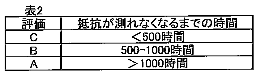
- the mounting substrate was subjected to a thermal cycle test at -40 to + 150 ° C.
- the substrate was taken out every 250 hours, the chip resistance was measured to confirm the continuity, and the time until the resistance could not be measured was measured.
- C was evaluated when resistance could not be measured before 500 hours passed, B when resistance could not be measured before 1000 hours, and A when resistance could be measured even after 1000 hours was evaluated.
- SYMBOLS 1 Laminated board for circuit boards, 1 '... metal base circuit board, 2 ... metal board, 3 ... insulation layer, 4 ... metal foil, 4' ... circuit pattern; 100: power module, 11: power device, 12: solder layer, 13: metal base circuit board, 13a: circuit pattern, 13b: insulating layer, 13c: metal substrate , 14 ... heat dissipation sheet, 15 ... heat sink; 200 ... conventional power module, 21 ... power device, 22 ... first solder layer, 23 ... circuit pattern, 24 ... ceramic substrate, 25 ... metallized layer, 26 ... Second solder layer, 27: Metal substrate, 28: Heat dissipation sheet, 29: Heat sink
Landscapes
- Engineering & Computer Science (AREA)
- Microelectronics & Electronic Packaging (AREA)
- Laminated Bodies (AREA)
- Insulated Metal Substrates For Printed Circuits (AREA)
- Chemical & Material Sciences (AREA)
- Ceramic Engineering (AREA)
- Cooling Or The Like Of Semiconductors Or Solid State Devices (AREA)
- Compositions Of Macromolecular Compounds (AREA)
Abstract
Description
図1及び図2に示す回路基板用積層板1は、金属基板2の片面に絶縁層3が形成され、絶縁層3の上に金属箔4が形成された3層構造をしている。本発明の他の形態において、金属板2の両面に絶縁層3が形成され、更に各絶縁層3の上に金属箔4が形成された5層構造をしていてもよい。なお、図1及び図2において、X及びY方向は金属基板2の主面に平行であり且つ互いに直交する方向であり、Z方向はX及びY方向に対して垂直な厚さ方向である。図1には、一例として矩形上の回路基板用積層板1を示しているが、回路基板用積層板1は他の形状を有していてもよい。
同じシアネート樹脂であっても、その分子構造のタイプによって硬化物のガラス転移温度(Tg)や、力学物性が異なるが、例えば、絶縁層の耐熱性と靭性を向上させるために単に高耐熱性樹脂と強靭性樹脂を併用して用いるだけでは所望とする高耐熱性と強靭性は得られない。強靭性のビスフェノール型シアネート樹脂と、高ガラス転移温度を有するノボラック型シアネート樹脂との架橋型共重合体を形成することにより、靭性に優れ、且つ、高耐熱性の絶縁層の提供が可能となる。これは、ノボラック型シアネート樹脂とビスフェノール型シアネート樹脂の混合物が架橋型共重合体構造をとることにより、ビスフェノール型単体で用いる場合よりも高ガラス転移温度となり、一方、ノボラック型シアネート樹脂の架橋構造にビスフェノール型シアネート樹脂の柔軟な構造が加わることにより、ノボラック型単体で用いる場合よりも靭性が向上するものと推測される。靱性が向上し、また、低弾性となることにより、絶縁層における、ヒートサイクルによるはんだ接続部への応力を間接的に緩和する性能(以下、「ヒートサイクル性能」ともいう)が高まる結果、はんだ接続信頼性を向上させることが可能となる。
リン系ボレート錯体の例として、テトラフェニルホスホニウムテトラフェニルボレート、テトラフェニルホスホニウムテトラ-p-トリルボレート、トリ-tert-ブチルホスホニウムテトラフェニルボレート、ジ-tert-ブチルメチルホスホニウムテトラフェニルボレート、p-トリルトリフェニルホスホニウムテトラ-p-トリルボレート、テトラフェニルホスホニウムテトラフルオロボレート、トリフェニルホスフィントリフェニルボレートなどが挙げられる。
金属基板2は、可撓性を有していてもよく、可撓性を有していなくてもよい。金属基板2の厚さは、例えば、0.2-5mmの範囲内にある。
金属箔4は、例えば、単体金属又は合金からなる。金属箔4の材料としては、例えば、銅又はアルミニウムを使用することができる。金属箔4の厚さは、例えば、10~500μmの範囲である。
まず、上述したビスフェノール型シアネート樹脂及びノボラック型シアネート樹脂と硬化促進剤を加熱混合し、その後溶剤に溶解させて溶液を得る。次に、上述した無機充填材を溶液中に分散させて分散液を得る。無機充填材は、例えば、ボールミル、三本ロール、遠心撹拌機又はビーズミルを用いて、粉砕しつつ上記溶液中に分散させてもよい。また、上記溶液に無機充填材を加えるのに先立って、この溶液にシランカップリング剤、イオン吸着剤などの添加剤を加えてもよい。
図3に示す金属ベース回路基板1´は、図1及び図2に示す回路基板用積層板から得られるものであり、金属基板2と、絶縁層3と、回路パターン4´とを含んでいる。回路パターン4´は、図1及び図2を参照しながら説明した回路基板用積層板の金属箔4をパターニングすることにより得られる。このパターニングは、例えば、金属箔4の上にマスクパターンを形成し、金属箔4の露出部をエッチングによって除去することにより得られる。金属ベース回路基板1´は、例えば、先の回路基板用積層板1の金属箔4に対して上記のパターニングを行い、必要に応じて、切断及び穴あけ加工などの加工を行うことにより得ることができる。
<組成物の調製>
合成例1:組成物1の調製
質量比が3:1になるようにビスフェノールA型シアネート樹脂(ロンザ製、「BA200」)とフェノールノボラック型シアネート樹脂(ロンザ製、「PT30」)を加熱混合し、樹脂量に対して1質量%のリン系硬化促進剤(テトラフェニルホスホニウムテトラボレート;北興化学製、「TPP-MK」)を混合した。その混合樹脂にジメチルアセトアミドを加えた樹脂固形分40質量%のシアネート樹脂溶液に対して、窒化ホウ素(水島合金鉄製、「HP-40」)と窒化アルミ(古河電子製(FAN-f30)を1:1の体積比で、樹脂固形分を基準として合計で65体積%となるよう配合し絶縁材溶液(組成物1)を作製した。
ビスフェノールA型シアネート樹脂(ロンザ製、「BA200」)とフェノールノボラック型シアネート樹脂(ロンザ製、「PT30」)の配合比を、表3に記載の通りに変更した以外は組成物1の調製方法と同様にして組成物2~5を作製した。
質量比が3:1になるようにビスフェノールA型シアネート樹脂(ロンザ製、「BA200」)とフェノールノボラック型シアネート樹脂(ロンザ製、「PT30」)を加熱混合し、樹脂量に対して1質量%のリン系硬化促進剤(北興化学製、「TPP-MK」)を混合した。その混合樹脂にジメチルアセトアミドを加えた樹脂固形分40質量%のシアネート樹脂溶液に対して、窒化硼素(水島合金鉄製、「HP-40」)とアルミナ(昭和電工製「AS40」)を1:1の体積比で、樹脂固形分を基準として合計で65体積%となるよう配合し絶縁材溶液(組成物6)を作製した。
質量比が3:1になるようにビスフェノールA型シアネート樹脂(ロンザ製、「BA200」)とフェノールノボラック型シアネート樹脂(ロンザ製、「PT30」)を加熱混合し、樹脂量に対して1質量%の非リン系硬化促進剤(ジアザビシクロノネンテトラフェニルボレート;北興化学製「DBNK」)を混合した。その混合樹脂にジメチルアセトアミドを加えた樹脂固形分40質量%のシアネート樹脂溶液に対して、窒化硼素(水島合金鉄製、「HP-40」)とアルミナ(昭和電工製「AS40」)を1:1の体積比で、樹脂固形分を基準として合計で65体積%となるよう配合し絶縁材溶液(組成物7)を作製した。
質量比が3:1になるようにビスフェノールA型シアネート樹脂(ロンザ製、「BA200」)とフェノールノボラック型シアネート樹脂(ロンザ製、「PT30」)を加熱混合し、樹脂量に対して1質量%のリン系硬化促進剤(北興化学製、「TPP-MK」)を混合した。その混合樹脂にジメチルアセトアミドを加えた樹脂固形分40質量%のシアネート樹脂溶液に対して、窒化硼素(水島合金鉄製、「HP-40」)とシランカップリング剤(信越化学製「KBM-103」)で表面処理したアルミナを1:1の体積比で、樹脂固形分を基準として合計で65体積%となるよう配合し絶縁材溶液(組成物8)を作製した。
質量比が3:1になるようにビスフェノールA型シアネート樹脂(ロンザ製、「BA200」)とフェノールノボラック型シアネート樹脂(ロンザ製、「PT30」)を加熱混合し、樹脂量に対して1質量%の非リン系硬化促進剤(北興化学製「DBNK」)を混合した。その混合樹脂にジメチルアセトアミドを加えた樹脂固形分40質量%のシアネート樹脂溶液に対して、窒化硼素(水島合金鉄製、「HP-40」)とシランカップリング剤(信越化学製「KBM-103」)で表面処理したアルミナを1:1の体積比で、樹脂固形分を基準として合計で65体積%となるよう配合し絶縁材溶液(組成物9)を作製した。
質量比が3:1になるようにビスフェノールA型シアネート樹脂(ロンザ製、「BA200」)とフェノールノボラック型シアネート樹脂(ロンザ製、「PT30」)を加熱混合し、樹脂量に対して1質量%の非リン系硬化促進剤(北興化学製「DBNK」)を混合した。その混合樹脂にジメチルアセトアミドを加えた樹脂固形分40質量%のシアネート樹脂溶液に対して、窒化硼素(水島合金鉄製、「HP-40」)と窒化アルミ(古河電子製(FAN-f30)を1:1の体積比で、樹脂固形分を基準として合計で65体積%となるよう配合し絶縁材溶液(組成物10)を作製した。
ビスフェノールA型シアネート樹脂(ロンザ製、「BA200」)とフェノールノボラック型シアネート樹脂(ロンザ製、「PT30」)の配合比を、表3に記載の通りに変更した以外は組成物1の調製方法と同様にして組成物11~15を作製した。
ビスフェノールA型シアネート樹脂(ロンザ製、「BA200」)と、樹脂量に対して1質量%のリン系硬化促進剤(北興化学製、「TPP-MK」)を混合した固形分40質量%のビスフェノールA型シアネート樹脂溶液(溶剤:ジメチルアセトアミド)に対して、窒化硼素(水島合金鉄製、「HP-40」)と窒化アルミ(古河電子製(FAN-f30)を1:1の体積比で、樹脂固形分を基準として合計で65体積%となるよう配合し絶縁材溶液(組成物1R)を作製した。
フェノールノボラック型シアネート樹脂(ロンザ製、「PT30」)と、樹脂量に対して1質量%のリン系硬化促進剤(北興化学製、「TPP-MK」)を混合した固形分40質量%のフェノールノボラック型シアネート樹脂溶液(溶剤:ジメチルアセトアミド)に対して、窒化硼素(水島合金鉄製、「HP-40」)と窒化アルミ(古河電子製(FAN-f30)を1:1の体積比で、樹脂固形分を基準として合計で65体積%となるよう配合し絶縁材溶液(組成物2R)を作製した。
[ガラス転移温度(Tg/℃)]
上述した方法により得られた各絶縁材溶液を、遊星式攪拌脱泡機で5分攪拌した後、厚み70μmの銅箔上に熱接着後の厚みが約100μmになるように塗布し、100℃で溶媒が無くなるまで乾燥した。この塗膜が形成された銅箔を、金属板として熱伝導率140W/mk、厚み2.0mmのアルミニウム合金板上に塗膜が中間層となるように積層し、圧力20MPa、温度250℃(但し、比較例3及び4は200℃)で熱接着した。得られた回路基板用積層板をサンプルとして、銅箔とアルミ板をケミカルエッチングして絶縁層のみを取り出した。
実施例1~15、比較例1~2の各樹脂組成において、無機フィラーを含まない状態で各樹脂及び硬化促進剤を溶融させた混合物を、シリコーン型に流し込み250℃(但し、比較例3及び4は200℃)で硬化させた後、2×10×41.5mmの試験片を作製し、ASTM d5045-93に従って破壊靭性値(MN/m3/2)を求めた。
上述した方法により得られた各絶縁材溶液を、遊星式攪拌脱泡機で5分攪拌した後、厚み70μmの銅箔上に熱接着後の厚みが約100μmになるように塗布し、100℃で溶媒が無くなるまで乾燥した。この塗膜が形成された銅箔を、金属板として熱伝導率140W/mk、厚み2.0mmのアルミニウム合金板上に塗膜が中間層となるように積層し、圧力20MPa、温度250℃(但し、比較例3及び4は200℃)で熱接着した。得られた回路基板用積層板をサンプルとして、吸湿耐熱性を以下の方法により評価した。

上述した方法により得られた各絶縁材溶液を、遊星式攪拌脱泡機で5分攪拌した後、厚み70μmの銅箔上に熱接着後の厚みが約100μmになるように塗布し、100℃で溶媒が無くなるまで乾燥した。この塗膜が形成された銅箔を、金属板として熱伝導率140W/mk、厚み2.0mmのアルミニウム合金板上に塗膜が中間層となるように積層し、圧力20MPa、温度250℃(但し、比較例3及び4は200℃)で熱接着した。得られた回路基板用積層板をサンプルとして、はんだ接続信頼性を以下の方法により評価した。

100・・・パワーモジュール、11・・・パワーデバイス、12・・・はんだ層、13・・・金属ベース回路基板、13a・・・回路パターン、13b・・・絶縁層、13c・・・金属基板、14・・・放熱シート、15・・・ヒートシンク;
200・・・従来のパワーモジュール、21・・・パワーデバイス、22・・・第一はんだ層、23・・・回路パターン、24・・・セラミック基板、25・・・メタライズ層、26・・・第二はんだ層、27・・・金属基板、28・・・放熱シート、29・・・ヒートシンク
Claims (10)
- 金属基板と、該金属基板の少なくとも片面に設けられた絶縁層と、該絶縁層上に設けられた金属箔とを具備する回路基板用積層板であって、前記絶縁層が、ビスフェノール型シアネート樹脂とノボラック型シアネート樹脂との架橋型共重合体及び無機充填材を含有することを特徴とする回路基板用積層板。
- 前記絶縁層に含有されるビスフェノール型シアネート樹脂とノボラック型シアネート樹脂の質量比が3:1~1:11である、請求項1に記載の回路基板用積層板。
- 前記絶縁層が更に硬化促進剤を含有する、請求項1又は2に記載の回路基板用積層板。
- 前記硬化促進剤がボレート錯体であり、前記無機充填材としてアルミナ、表面処理されたアルミナ、窒化アルミ及び窒化ホウ素から選択される少なくとも1種を含有する、請求項3に記載の回路基板用積層板。
- 前記硬化促進剤がリン系ボレート錯体であり、前記無機充填材として表面処理されたアルミナ、窒化アルミ及び窒化ホウ素から選択される少なくとも1種を含有する、請求項4に記載の回路基板用積層板。
- 前記無機充填材として、表面処理されたアルミナ、窒化アルミ及び窒化ホウ素から選択される2種以上を含有する、請求項5に記載の回路基板用積層板。
- 前記硬化促進剤が非リン系ボレート錯体であり、前記無機充填材としてアルミナ、表面処理されたアルミナ、窒化アルミ及び窒化ホウ素から選択される少なくとも1種を含有する、請求項4に記載の回路基板用積層板。
- 前記無機充填材として、アルミナ、表面処理されたアルミナ、窒化アルミ及び窒化ホウ素から選択される2種以上を含有する、請求項7に記載の回路基板用積層板。
- 請求項1~8のいずれか1項に記載の回路基板用積層板が具備する金属箔をパターニングすることによって得られる金属ベース回路基板。
- 請求項9に記載の金属ベース回路基板を備えるパワーモジュール。
Priority Applications (6)
| Application Number | Priority Date | Filing Date | Title |
|---|---|---|---|
| CN201380035886.7A CN104412721B (zh) | 2012-07-06 | 2013-07-04 | 电路基板用层叠板、金属基底电路基板及电源模块 |
| EP13813816.9A EP2871918B1 (en) | 2012-07-06 | 2013-07-04 | Laminate for circuit boards, metal-based circuit board, and power module |
| JP2014523783A JP5895055B2 (ja) | 2012-07-06 | 2013-07-04 | 回路基板用積層板、金属ベース回路基板及びパワーモジュール |
| KR1020157003145A KR101766552B1 (ko) | 2012-07-06 | 2013-07-04 | 회로 기판용 적층판, 금속 베이스 회로 기판 및 파워 모듈 |
| US14/589,531 US20150118509A1 (en) | 2012-07-06 | 2015-01-05 | Circuit board laminate, metal base circuit board and power module |
| US16/147,324 US20190037692A1 (en) | 2012-07-06 | 2018-09-28 | Method of manufacturing a circuit board laminate |
Applications Claiming Priority (2)
| Application Number | Priority Date | Filing Date | Title |
|---|---|---|---|
| JP2012152970 | 2012-07-06 | ||
| JP2012-152970 | 2012-07-06 |
Related Child Applications (1)
| Application Number | Title | Priority Date | Filing Date |
|---|---|---|---|
| US14/589,531 Continuation US20150118509A1 (en) | 2012-07-06 | 2015-01-05 | Circuit board laminate, metal base circuit board and power module |
Publications (1)
| Publication Number | Publication Date |
|---|---|
| WO2014007327A1 true WO2014007327A1 (ja) | 2014-01-09 |
Family
ID=49882078
Family Applications (1)
| Application Number | Title | Priority Date | Filing Date |
|---|---|---|---|
| PCT/JP2013/068361 Ceased WO2014007327A1 (ja) | 2012-07-06 | 2013-07-04 | 回路基板用積層板、金属ベース回路基板及びパワーモジュール |
Country Status (7)
| Country | Link |
|---|---|
| US (2) | US20150118509A1 (ja) |
| EP (1) | EP2871918B1 (ja) |
| JP (2) | JP5895055B2 (ja) |
| KR (1) | KR101766552B1 (ja) |
| CN (1) | CN104412721B (ja) |
| TW (1) | TWI522017B (ja) |
| WO (1) | WO2014007327A1 (ja) |
Cited By (4)
| Publication number | Priority date | Publication date | Assignee | Title |
|---|---|---|---|---|
| EP2952539A1 (en) * | 2014-06-05 | 2015-12-09 | Shin-Etsu Chemical Co., Ltd. | Heat-curable resin composition |
| JP2016143775A (ja) * | 2015-02-02 | 2016-08-08 | 日本発條株式会社 | 金属ベース回路基板及びその製造方法 |
| JP2018207041A (ja) * | 2017-06-08 | 2018-12-27 | 日本発條株式会社 | 回路基板用積層板、金属ベース回路基板及びパワーモジュール |
| WO2019112048A1 (ja) * | 2017-12-08 | 2019-06-13 | 積水化学工業株式会社 | 積層体及び電子装置 |
Families Citing this family (6)
| Publication number | Priority date | Publication date | Assignee | Title |
|---|---|---|---|---|
| JP1602558S (ja) * | 2017-04-25 | 2018-04-23 | ||
| CN110546758B (zh) * | 2017-06-23 | 2023-09-19 | 积水化学工业株式会社 | 散热片、散热片的制造方法以及叠层体 |
| EP3950763B1 (en) * | 2019-03-27 | 2025-10-22 | NHK Spring Co., Ltd. | Thermosetting epoxy resin composition, layered sheet for circuit board, metal-based circuit board, and power module |
| CN111524814B (zh) * | 2020-03-30 | 2022-02-11 | 中国电子科技集团公司第二十九研究所 | 一种功率器件高可靠高密度集成结构的制备方法 |
| KR102870606B1 (ko) * | 2020-06-17 | 2025-10-15 | 엘지이노텍 주식회사 | 회로기판 |
| TWI762290B (zh) * | 2021-04-28 | 2022-04-21 | 璦司柏電子股份有限公司 | 具複數功率元件電源模組的間隔加壓結合法 |
Citations (8)
| Publication number | Priority date | Publication date | Assignee | Title |
|---|---|---|---|---|
| JP2004202895A (ja) | 2002-12-25 | 2004-07-22 | Sumitomo Bakelite Co Ltd | 絶縁シート、金属箔付き絶縁シートおよび多層プリント配線板 |
| JP2005272573A (ja) | 2004-03-24 | 2005-10-06 | Sumitomo Bakelite Co Ltd | 樹脂組成物、プリプレグおよび積層板 |
| JP2008098489A (ja) | 2006-10-13 | 2008-04-24 | Matsushita Electric Ind Co Ltd | 熱伝導基板とその製造方法 |
| JP2010031263A (ja) | 2008-06-30 | 2010-02-12 | Sumitomo Bakelite Co Ltd | エポキシ樹脂組成物、プリプレグ、積層板、樹脂シート、多層プリント配線板、及び半導体装置 |
| JP2010174242A (ja) * | 2009-12-28 | 2010-08-12 | Sumitomo Bakelite Co Ltd | ビフェニルアラルキル型シアン酸エステル樹脂、並びにビフェニルアラルキル型シアン酸エステル樹脂を含む樹脂組成物、及び、当該樹脂組成物を用いてなるプリプレグ、積層板、樹脂シート、多層プリント配線板、並びに半導体装置 |
| KR20100103942A (ko) * | 2009-03-16 | 2010-09-29 | (주)켐텍 | 에폭시 수지 조성물 및 이를 이용하여 제조된 프린트 배선판용 접착 필름 |
| JP2011116910A (ja) | 2009-12-07 | 2011-06-16 | Sumitomo Bakelite Co Ltd | 回路基板用樹脂組成物、プリプレグ、積層板、樹脂シート、多層プリント配線板および半導体装置 |
| JP2011249606A (ja) * | 2010-05-27 | 2011-12-08 | Nhk Spring Co Ltd | 回路基板用積層板及び金属ベース回路基板 |
Family Cites Families (14)
| Publication number | Priority date | Publication date | Assignee | Title |
|---|---|---|---|---|
| US6097089A (en) * | 1998-01-28 | 2000-08-01 | Mitsubishi Gas Chemical Company, Inc. | Semiconductor plastic package, metal plate for said package, and method of producing copper-clad board for said package |
| JPH1112463A (ja) * | 1997-06-27 | 1999-01-19 | Hitachi Chem Co Ltd | 印刷配線板用樹脂組成物、ワニス、プリプレグ及びそれを用いた印刷配線板用積層板 |
| SG73590A1 (en) * | 1997-12-03 | 2000-06-20 | Sumitomo Bakelite Co | Latent catalyst thermosetting resin composition comprising the catalyst epoxy resin molding material comprising the catalyst and semiconductor device |
| JP2000191776A (ja) * | 1998-12-24 | 2000-07-11 | Mitsubishi Gas Chem Co Inc | シアン酸エステル・コ−プレポリマー |
| JP4075268B2 (ja) * | 2000-02-24 | 2008-04-16 | 松下電工株式会社 | 回路基板の製造方法 |
| JP2002069152A (ja) * | 2000-08-24 | 2002-03-08 | Japan Epoxy Resin Kk | プリント配線板用エポキシ樹脂組成物およびプリント配線板 |
| JP4407823B2 (ja) * | 2004-02-18 | 2010-02-03 | 三菱瓦斯化学株式会社 | 新規なシアネートエステル化合物、難燃性樹脂組成物、およびその硬化物 |
| DE102006033987A1 (de) * | 2006-07-22 | 2008-01-24 | Continental Aktiengesellschaft | Zubringereinrichtung |
| JP2010090237A (ja) * | 2008-10-07 | 2010-04-22 | Ajinomoto Co Inc | エポキシ樹脂組成物 |
| US8658719B2 (en) * | 2009-06-11 | 2014-02-25 | Arlon | Low loss pre-pregs and laminates and compositions useful for the preparation thereof |
| CN102482481B (zh) * | 2009-07-24 | 2014-12-17 | 住友电木株式会社 | 树脂组合物,树脂片材,半固化片,覆金属层叠板,印刷布线板及半导体装置 |
| JP2011099072A (ja) * | 2009-11-09 | 2011-05-19 | Sumitomo Bakelite Co Ltd | 樹脂組成物、絶縁層、プリプレグ、積層板、プリント配線板および半導体装置 |
| JP5861995B2 (ja) * | 2010-07-05 | 2016-02-16 | 住友ベークライト株式会社 | 樹脂組成物、プリプレグ、樹脂層、回路基板および半導体装置 |
| US9279051B2 (en) * | 2011-09-22 | 2016-03-08 | Elite Material Co., Ltd. | Halogen-free resin composition, and copper clad laminate and printed circuit board using same |
-
2013
- 2013-07-04 EP EP13813816.9A patent/EP2871918B1/en active Active
- 2013-07-04 JP JP2014523783A patent/JP5895055B2/ja active Active
- 2013-07-04 CN CN201380035886.7A patent/CN104412721B/zh active Active
- 2013-07-04 WO PCT/JP2013/068361 patent/WO2014007327A1/ja not_active Ceased
- 2013-07-04 KR KR1020157003145A patent/KR101766552B1/ko active Active
- 2013-07-05 TW TW102124184A patent/TWI522017B/zh active
-
2015
- 2015-01-05 US US14/589,531 patent/US20150118509A1/en not_active Abandoned
- 2015-12-08 JP JP2015239480A patent/JP6223407B2/ja active Active
-
2018
- 2018-09-28 US US16/147,324 patent/US20190037692A1/en not_active Abandoned
Patent Citations (8)
| Publication number | Priority date | Publication date | Assignee | Title |
|---|---|---|---|---|
| JP2004202895A (ja) | 2002-12-25 | 2004-07-22 | Sumitomo Bakelite Co Ltd | 絶縁シート、金属箔付き絶縁シートおよび多層プリント配線板 |
| JP2005272573A (ja) | 2004-03-24 | 2005-10-06 | Sumitomo Bakelite Co Ltd | 樹脂組成物、プリプレグおよび積層板 |
| JP2008098489A (ja) | 2006-10-13 | 2008-04-24 | Matsushita Electric Ind Co Ltd | 熱伝導基板とその製造方法 |
| JP2010031263A (ja) | 2008-06-30 | 2010-02-12 | Sumitomo Bakelite Co Ltd | エポキシ樹脂組成物、プリプレグ、積層板、樹脂シート、多層プリント配線板、及び半導体装置 |
| KR20100103942A (ko) * | 2009-03-16 | 2010-09-29 | (주)켐텍 | 에폭시 수지 조성물 및 이를 이용하여 제조된 프린트 배선판용 접착 필름 |
| JP2011116910A (ja) | 2009-12-07 | 2011-06-16 | Sumitomo Bakelite Co Ltd | 回路基板用樹脂組成物、プリプレグ、積層板、樹脂シート、多層プリント配線板および半導体装置 |
| JP2010174242A (ja) * | 2009-12-28 | 2010-08-12 | Sumitomo Bakelite Co Ltd | ビフェニルアラルキル型シアン酸エステル樹脂、並びにビフェニルアラルキル型シアン酸エステル樹脂を含む樹脂組成物、及び、当該樹脂組成物を用いてなるプリプレグ、積層板、樹脂シート、多層プリント配線板、並びに半導体装置 |
| JP2011249606A (ja) * | 2010-05-27 | 2011-12-08 | Nhk Spring Co Ltd | 回路基板用積層板及び金属ベース回路基板 |
Non-Patent Citations (1)
| Title |
|---|
| See also references of EP2871918A4 |
Cited By (16)
| Publication number | Priority date | Publication date | Assignee | Title |
|---|---|---|---|---|
| EP2952539A1 (en) * | 2014-06-05 | 2015-12-09 | Shin-Etsu Chemical Co., Ltd. | Heat-curable resin composition |
| JP2016011410A (ja) * | 2014-06-05 | 2016-01-21 | 信越化学工業株式会社 | 熱硬化性樹脂組成物 |
| US9382421B2 (en) | 2014-06-05 | 2016-07-05 | Shin-Etsu Chemical Co., Ltd. | Heat-curable resin composition |
| CN107211530B (zh) * | 2015-02-02 | 2020-07-10 | 日本发条株式会社 | 金属底座电路基板及其制造方法 |
| WO2016125650A1 (ja) * | 2015-02-02 | 2016-08-11 | 日本発條株式会社 | 金属ベース回路基板及びその製造方法 |
| CN107211530A (zh) * | 2015-02-02 | 2017-09-26 | 日本发条株式会社 | 金属底座电路基板及其制造方法 |
| JP2016143775A (ja) * | 2015-02-02 | 2016-08-08 | 日本発條株式会社 | 金属ベース回路基板及びその製造方法 |
| US11490513B2 (en) | 2015-02-02 | 2022-11-01 | Nhk Spring Co., Ltd. | Metal base circuit board and method of manufacturing the metal base circuit board |
| JP2018207041A (ja) * | 2017-06-08 | 2018-12-27 | 日本発條株式会社 | 回路基板用積層板、金属ベース回路基板及びパワーモジュール |
| JP7262918B2 (ja) | 2017-06-08 | 2023-04-24 | 日本発條株式会社 | 回路基板用積層板、金属ベース回路基板及びパワーモジュール |
| WO2019112048A1 (ja) * | 2017-12-08 | 2019-06-13 | 積水化学工業株式会社 | 積層体及び電子装置 |
| KR20200092932A (ko) * | 2017-12-08 | 2020-08-04 | 세키스이가가쿠 고교가부시키가이샤 | 적층체 및 전자 장치 |
| JPWO2019112048A1 (ja) * | 2017-12-08 | 2020-10-08 | 積水化学工業株式会社 | 積層体及び電子装置 |
| US11798863B2 (en) | 2017-12-08 | 2023-10-24 | Sekisui Chemical Co., Ltd. | Laminate and electronic device |
| JP7406372B2 (ja) | 2017-12-08 | 2023-12-27 | 積水化学工業株式会社 | 積層体及び電子装置 |
| KR102737282B1 (ko) * | 2017-12-08 | 2024-12-05 | 세키스이가가쿠 고교가부시키가이샤 | 적층체 및 전자 장치 |
Also Published As
| Publication number | Publication date |
|---|---|
| JP5895055B2 (ja) | 2016-03-30 |
| EP2871918A4 (en) | 2016-03-16 |
| CN104412721B (zh) | 2018-07-27 |
| EP2871918B1 (en) | 2021-09-08 |
| KR20150036408A (ko) | 2015-04-07 |
| US20190037692A1 (en) | 2019-01-31 |
| KR101766552B1 (ko) | 2017-08-08 |
| CN104412721A (zh) | 2015-03-11 |
| JPWO2014007327A1 (ja) | 2016-06-02 |
| JP6223407B2 (ja) | 2017-11-01 |
| TWI522017B (zh) | 2016-02-11 |
| EP2871918A1 (en) | 2015-05-13 |
| TW201419952A (zh) | 2014-05-16 |
| US20150118509A1 (en) | 2015-04-30 |
| JP2016106395A (ja) | 2016-06-16 |
Similar Documents
| Publication | Publication Date | Title |
|---|---|---|
| JP5895055B2 (ja) | 回路基板用積層板、金属ベース回路基板及びパワーモジュール | |
| JP7202690B2 (ja) | 樹脂組成物、基材付フィルム、金属/樹脂積層体および半導体装置 | |
| JP4495768B2 (ja) | 絶縁シート及び積層構造体 | |
| CN105051111B (zh) | 树脂组合物以及采用其得到的粘接膜、覆盖膜、层间粘接剂 | |
| KR102900411B1 (ko) | 수지 조성물 | |
| JP5109411B2 (ja) | 電子機器用接着剤組成物およびそれを用いた電子機器用接着剤シート、電子部品 | |
| JPWO2016125664A1 (ja) | 樹脂組成物 | |
| KR102946978B1 (ko) | 수지 조성물 | |
| JP2003286391A (ja) | エポキシ樹脂組成物、ワニス、このエポキシ樹脂組成物を用いたフィルム状接着剤及びその硬化物 | |
| JP2005307152A (ja) | 熱硬化性接着剤用組成物及びそれを用いた電子部品用接着テープ | |
| JP2003193016A (ja) | 高耐熱高放熱接着フィルム | |
| JP2022110408A (ja) | 樹脂組成物、及び、熱伝導性シート | |
| KR101866561B1 (ko) | 성형성이 우수한 에폭시 수지 조성물 및 이를 포함한 금속 베이스 인쇄회로기판용 적층체 | |
| JP7262918B2 (ja) | 回路基板用積層板、金属ベース回路基板及びパワーモジュール | |
| TWI686446B (zh) | 樹脂組成物、電路基板用積層板、金屬基底電路基板及電力模組 | |
| JP2013254922A (ja) | 金属ベース回路基板 | |
| JP2004256631A (ja) | 接着剤組成物及び接着フィルム | |
| KR20240151204A (ko) | 층간 절연용 에폭시 수지 조성물, 층간 절연용 수지 시트, 회로 기판용 적층체, 금속 베이스 회로 기판 및 파워 모듈 | |
| WO2025197972A1 (ja) | 熱硬化性組成物、熱硬化性シートの製造方法、熱伝導性シート、放熱積層体、放熱性回路基板及びパワー半導体装置 | |
| JP2017171890A (ja) | 樹脂組成物、熱硬化性フィルム、硬化物、プリント配線板、半導体装置 | |
| TW202502893A (zh) | 樹脂組成物 | |
| WO2025182894A1 (ja) | 絶縁シート、絶縁シートの製造方法、及び半導体装置 | |
| JP2005209913A (ja) | 極薄フレキシブル配線板 | |
| WO2025204162A1 (ja) | 樹脂組成物、それを用いた熱硬化性フィルム、熱硬化性フィルムの硬化物、及び半導体装置 | |
| JP2013254919A (ja) | 回路基板及び電子部品搭載基板 |
Legal Events
| Date | Code | Title | Description |
|---|---|---|---|
| 121 | Ep: the epo has been informed by wipo that ep was designated in this application |
Ref document number: 13813816 Country of ref document: EP Kind code of ref document: A1 |
|
| DPE1 | Request for preliminary examination filed after expiration of 19th month from priority date (pct application filed from 20040101) | ||
| ENP | Entry into the national phase |
Ref document number: 2014523783 Country of ref document: JP Kind code of ref document: A |
|
| NENP | Non-entry into the national phase |
Ref country code: DE |
|
| ENP | Entry into the national phase |
Ref document number: 20157003145 Country of ref document: KR Kind code of ref document: A |
|
| WWE | Wipo information: entry into national phase |
Ref document number: 2013813816 Country of ref document: EP |