WO2014010035A1 - Connecteur optique et serveur utilisant un connecteur optique - Google Patents
Connecteur optique et serveur utilisant un connecteur optique Download PDFInfo
- Publication number
- WO2014010035A1 WO2014010035A1 PCT/JP2012/067641 JP2012067641W WO2014010035A1 WO 2014010035 A1 WO2014010035 A1 WO 2014010035A1 JP 2012067641 W JP2012067641 W JP 2012067641W WO 2014010035 A1 WO2014010035 A1 WO 2014010035A1
- Authority
- WO
- WIPO (PCT)
- Prior art keywords
- connector
- optical
- connector member
- housing
- magnet
- Prior art date
- Legal status (The legal status is an assumption and is not a legal conclusion. Google has not performed a legal analysis and makes no representation as to the accuracy of the status listed.)
- Ceased
Links
Images


Classifications
-
- G—PHYSICS
- G02—OPTICS
- G02B—OPTICAL ELEMENTS, SYSTEMS OR APPARATUS
- G02B6/00—Light guides; Structural details of arrangements comprising light guides and other optical elements, e.g. couplings
- G02B6/24—Coupling light guides
- G02B6/36—Mechanical coupling means
- G02B6/38—Mechanical coupling means having fibre to fibre mating means
- G02B6/3807—Dismountable connectors, i.e. comprising plugs
- G02B6/389—Dismountable connectors, i.e. comprising plugs characterised by the method of fastening connecting plugs and sockets, e.g. screw- or nut-lock, snap-in, bayonet type
-
- G—PHYSICS
- G02—OPTICS
- G02B—OPTICAL ELEMENTS, SYSTEMS OR APPARATUS
- G02B6/00—Light guides; Structural details of arrangements comprising light guides and other optical elements, e.g. couplings
- G02B6/24—Coupling light guides
- G02B6/26—Optical coupling means
- G02B6/32—Optical coupling means having lens focusing means positioned between opposed fibre ends
-
- G—PHYSICS
- G02—OPTICS
- G02B—OPTICAL ELEMENTS, SYSTEMS OR APPARATUS
- G02B6/00—Light guides; Structural details of arrangements comprising light guides and other optical elements, e.g. couplings
- G02B6/24—Coupling light guides
- G02B6/36—Mechanical coupling means
- G02B6/38—Mechanical coupling means having fibre to fibre mating means
- G02B6/3807—Dismountable connectors, i.e. comprising plugs
- G02B6/3873—Connectors using guide surfaces for aligning ferrule ends, e.g. tubes, sleeves, V-grooves, rods, pins, balls
- G02B6/3886—Magnetic means to align ferrule ends
-
- G—PHYSICS
- G02—OPTICS
- G02B—OPTICAL ELEMENTS, SYSTEMS OR APPARATUS
- G02B6/00—Light guides; Structural details of arrangements comprising light guides and other optical elements, e.g. couplings
- G02B6/24—Coupling light guides
- G02B6/42—Coupling light guides with opto-electronic elements
- G02B6/4201—Packages, e.g. shape, construction, internal or external details
- G02B6/4246—Bidirectionally operating package structures
-
- G—PHYSICS
- G02—OPTICS
- G02B—OPTICAL ELEMENTS, SYSTEMS OR APPARATUS
- G02B6/00—Light guides; Structural details of arrangements comprising light guides and other optical elements, e.g. couplings
- G02B6/24—Coupling light guides
- G02B6/42—Coupling light guides with opto-electronic elements
- G02B6/4292—Coupling light guides with opto-electronic elements the light guide being disconnectable from the opto-electronic element, e.g. mutually self aligning arrangements
-
- G—PHYSICS
- G02—OPTICS
- G02B—OPTICAL ELEMENTS, SYSTEMS OR APPARATUS
- G02B6/00—Light guides; Structural details of arrangements comprising light guides and other optical elements, e.g. couplings
- G02B6/24—Coupling light guides
- G02B6/42—Coupling light guides with opto-electronic elements
- G02B6/43—Arrangements comprising a plurality of opto-electronic elements and associated optical interconnections
Definitions
- the present invention relates to an optical connector, and more particularly to a movable optical connector used when wiring is connected by a plurality of connectors in signal transmission / reception between a substrate and another substrate.
- an optical signal from an optical transmission / reception module that performs photoelectric conversion (or electro-optical conversion) is formed when an optical signal transmission system is configured.
- the connection method between optical connectors connected to one end of the transmitting optical fiber or the optical waveguide becomes a problem.
- the first In order to increase the practicality by optically connecting the optical connector and the optical connector, which are the exits of the optical signal output from the unit substrate having the LSI and electrical wiring laid on the substrate, with sufficient accuracy, the first In addition, it is necessary that the optical axis alignment between the optical connector and the optical connector composed of a plurality of optical fibers or optical waveguides can be achieved with sufficient accuracy.
- the allowable amount of optical axis deviation is, for example, 20 ⁇ m or less when the optical transmission line such as an optical fiber or an optical waveguide is a multimode optical waveguide.
- considering mass production of products it is necessary to be able to position and fix with high workability and high accuracy without performing complicated optical axis adjustment work.
- connection on which means coupling of optical connectors or connection off which means disconnection of connections can be easily performed, and there is a failure part. It is necessary to easily replace only the unit substrate.
- FIG. 18 is a schematic cross-sectional view of a widely used optical connector.
- the connection is made using guide pins or housing guides attached to the optical connector.
- the optical connector and the optical connector are automatically aligned without adjustment by a so-called fitting method. Therefore, the first requirement and the second requirement can be satisfied.
- a method of connecting an optical connector and an optical connector using a magnet as an alignment mark is known (for example, see Patent Document 1).
- a magnet is mounted on one connector.
- the magnet also has a function as an alignment mark for performing high-precision alignment between the connector and the connector.
- the optical connector and the optical connector are optically coupled. Also in this structure, since the optical axis alignment of the optical connector and the optical connector is automatically achieved without adjustment (self-alignment), it is possible to satisfy the first requirement and the second requirement.
- connection between the plurality of unit boards is performed via the inter-substrate wiring formed on the rear substrate, connection between a large number of circuit elements is particularly required.
- the number of wirings in a board and between boards increases, and the increase in the number of wirings causes a problem of wiring congestion and mutual interference between wirings.
- the cooling system for cooling the unit board may not function due to wiring congestion.
- the connection between the unit substrates via the inter-board wiring formed on the back substrate causes an increase or variation in the inter-circuit element wiring length, which causes an increase in signal delay and a clock skew.
- an optical connector of the present invention is, for example, an optical connector including a first connector member and a second connector member
- the first connector member includes a housing and a housing.
- the second connector member includes a housing An optical fiber through hole passing through the housing, a fixing portion for fixing the optical fiber provided in the housing, and a second alignment portion provided on the surface of the housing, the first alignment portion
- a magnet is provided in a portion connected to the second alignment portion on the surface of the first
- a magnetic body is provided in a portion connected to the magnet on the surface of the second alignment portion, the magnet of the first connector member, By connecting the magnetic body of the 2 connector member, By connecting the member members together, the optical fiber fixed to the first connector member and the optical fiber fixed to the second connector member are optically connected. It further has a shielding means.
- an optical connector that can be easily connected and disconnected between connectors even when the number of connectors is plural.
- an optical connector it is a figure explaining the state (a) in which a connection between optical connectors is on, and the state (b) in which a connection between optical connectors is off. It is a figure explaining the signal transmission / reception performed between the unit board
- a control lever installed at each terminal is used to connect and disconnect the connector. It is a figure explaining the server using the optical connector and several unit board
- an optical connector it is a figure explaining the state (a) in which a connection between optical connectors is on, and the state (b) in which a connection between optical connectors is off. It is a figure explaining the basic composition of the optical connector by the 2nd Embodiment of this invention. In an optical connector, it is a figure explaining the state (a) in which a connection between optical connectors is on, and the state (b) in which a connection between optical connectors is off. It is a figure explaining the basic composition of the optical connector by the 3rd Embodiment of this invention. In an optical connector, it is a figure explaining the state (a) in which a connection between optical connectors is on, and the state (b) in which a connection between optical connectors is off.
- an optical connector it is a figure explaining the state (a) in which a connection between optical connectors is on, and the state (b) in which a connection between optical connectors is off. It is a figure explaining the basic composition of the optical connector by the 8th Embodiment of this invention. In an optical connector, it is a figure explaining the state (a) in which a connection between optical connectors is on, and the state (b) in which a connection between optical connectors is off. It is a figure explaining the basic composition of the optical connector by a 9th embodiment of the present invention. In an optical connector, it is a figure explaining the state (a) in which a connection between optical connectors is on, and the state (b) in which a connection between optical connectors is off.
- an optical connector device having a magnetic shielding means and having a self-alignment magnet mechanism will be described.
- the magnetic shielding means referred to in this specification means means for weakening the magnetic force acting between the magnet and the metal.
- the configuration in which this means is realized will be described in each embodiment.
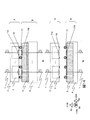
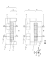
- FIG. 1A and 1B are configuration diagrams of an optical connector device according to the present embodiment, where FIG. 1A shows a connector connection state, and FIG. 1B shows a connector disconnection state.
- FIG. 2 is an enlarged view of a connection portion between the connectors in FIG. 1, (a) shows a connection state between the magnet and the magnetic material, and (b) shows a separation state between the magnet and the magnetic material.
- the connector member A is composed of a connector housing and a receptacle which is an alignment unit.
- a through hole for passing an optical fiber and a fixing portion for fixing the optical fiber are provided in the connector housing.
- the connector member B includes a connector housing and a receptacle.
- the receptacle is configured to fit on a rail attached to the connector housing, the receptacle can be freely moved out and retracted with respect to the connector housing. It has become. With this structure, even when the connector member A and the connector member B are fixed to a server blade or the like, the connection on state can be realized by moving only the receptacle from the connection off state between these connectors.
- one of the receptacles of the connector member A and the connector member B has a magnetic shielding means, and a magnet is provided instead of the alignment mark. Both connector members are aligned by the attractive force between the magnet and a magnetic material such as metal, and the connected state is maintained.
- lenses 11a and 11b are attached to the connector member A and the connector member B, respectively.
- this lens for example, the light emitted from the connector optical fiber becomes collimated light having an enlarged beam size, propagates through the space, and when the light is input to the optical fiber, the enlarged light beam is condensed by the lens 11b. And coupled with the optical fiber.
- the connection tolerance accuracy between the connector member A and the connector member B is increased 10 times or more, and is less susceptible to dust and dirt in the atmosphere.
- the connector state of the connector member A and the connector member B is maintained by the magnet mechanism, and the connector member A and the connector member B are held by the magnetic shielding means as shown in FIG. Is cut off.
- An optical signal has a bandwidth by encoding information in a plurality of frequency components of light transmitted along one optical fiber or a waveguide using wavelength division multiplexing (Wave Division Multiplexing: WDM). It may be enhanced.
- WDM wavelength division multiplexing
- the optical transmission medium may comprise a plurality of optical fibers or waveguides. Thereby, each optical fiber or waveguide carries a WDM signal and realizes a high bandwidth per unit area.
- FIG. 2 explains the details of the connection location between the connectors shown in FIG.
- the magnet 22 has a structure capable of rotating. It can be controlled manually. Specifically, when the straight line connecting the N pole side and the S pole side of the magnet is parallel to the magnetic material, the lines of magnetic force enter the magnetic material through the yoke 21, and therefore the attractive force between the magnet and the magnetic material. Works, and the magnet and the magnetic material are attached.
- FIG. 2B when the straight line connecting the north and south poles of the magnet is perpendicular to the magnetic material, the magnetic force lines cannot enter the magnetic material and the magnet and the magnetic material are separated. It becomes a state. Thus, by rotating the magnet, the magnet and the magnetic material can be connected and disconnected.
- 1A and 1B illustrate a case where this mechanism is employed.
- the movement of the connector member A and the connector member B is in the x, y, z directions, the inclination angles, and the rotation angles ⁇ a, ⁇ b, ⁇ c, respectively, and the connection between the connector member A and the connector member B is Alignment adjustment is performed with high accuracy so as to achieve a highly efficient optical coupling state.
- the configuration of the present embodiment is an optical connector including a first connector member A and a second connector member B.
- the first connector member A includes a housing 2 and a housing 2. A through hole for an optical fiber passing through the inside, a fixing portion for fixing the optical fiber 1 provided in the housing 2, and a first alignment portion 3 provided on the surface of the housing 2.
- the connector member B includes a housing 6, an optical fiber through hole passing through the housing 6, a fixing portion for fixing the optical fiber 1 provided in the housing 6, and a first provided on the surface of the housing 6.
- the second alignment unit 5 is provided with a magnet on the surface of the first alignment unit 3 connected to the second alignment unit, and the second alignment unit 5 is connected to the surface of the magnet.
- the part 3 further includes magnetic shielding means.
- the magnet terminal to be the alignment mark can be formed by patterning, it can be formed with high precision. Since the patterned magnets are in contact with each other, a force is automatically exerted in a direction to correct the misalignment. Since it is not necessary to adopt a special means for high precision connection of the connector, it is possible to save the connector space.
- FIG. 3A and 3B are configuration diagrams of the optical connector device according to the present embodiment, where FIG. 3A shows a state before connector connection, and FIG. 3B shows a state after connector connection.
- the connector member 102 and the connector member 108 achieve high-efficiency optical coupling by combining a magnet that also serves as an opposing alignment mark and a magnetic material. That is, as shown in FIG. 3A, the mark 103a on the connector member 102 side and the mark 106a on the connector member 108 side, and similarly 103b and 106b, 103c and 106c, 103d and 106d, 103e and 106e, 103f And the alignment marks 106f are matched to achieve high-precision optical connector connection.
- the connection state between the connector member 102 and the connector member 108 is held, for example, by the attractive force of the magnet and the magnetic material in the magnet mechanism.
- signal exchange between the optical transceiver modules is performed as follows.
- a signal generated from the optical transmission / reception module 101 is transmitted through the optical fiber 109, passes through the connector member 102 and the connector member 108 connected in a highly efficient optical coupling state, and then again passes through the optical fiber 109 to the opposing optical transmission / reception module 101. Sent and detected.
- the mechanism shown in the first embodiment may be applied to the receptacle (not shown), but the magnetic shielding means is not limited to this.
- FIG. 4 is a block diagram showing signal transmission / reception between substrates using the optical connector according to the present embodiment.
- Signal transmission and reception is as follows. An electrical signal from the electronic component 185 of the substrate 150 is first sent to the optical module 184 through the wiring 183, and is converted into an optical signal by performing an electrical-optical conversion in the optical module 184, and then transmitted through an optical fiber. After being sent to the optical fiber again through the optical connector members 161 and 166 and subjected to optical-electrical conversion by the optical module 184 and converted into an electrical signal, the CPU mounted on the other board 151 It is sent to an electronic component 185 such as a memory controller. In this way, signal transmission / reception is realized by optical signal transmission / reception between electronic components mounted on different substrates.
- large-capacity signal transmission / reception is realized by performing signal transmission / reception between electronic components mounted on different substrates using optical wiring using a plurality of optical connectors. That is, even through the optical connector members 162 and 165, large-capacity signal transmission / reception is realized by performing signal transmission / reception between electronic components mounted on different substrates using optical wiring. Similarly, large-capacity signal transmission / reception is realized by performing signal transmission / reception between the electronic components mounted on different substrates through the optical wiring also through the optical connector members 163 and 164. In general, the number of optical connectors increases as the capacity of signals to be processed increases.
- the movement of the connector members 161, 162, 163, 164, 165, and 166 becomes the x, y, z directions, the inclination angle, and the rotation angle ⁇ as shown in FIG.
- the connection is aligned with high accuracy so as to be in a highly efficient optical coupling state.
- the connection between the connector member 162 and the connector member 165 and the connection between the connector member 163 and the connector member 164 are made with high accuracy.
- the mechanism shown in the first embodiment may be applied to the receptacle (not shown), but the shielding means is not limited to this.
- FIG. 5 is a block diagram showing signal transmission / reception between boards using the optical connector device according to the present embodiment.
- Signal transmission and reception is as follows.
- An electrical signal from the electronic component 185 of the substrate 150 is first sent to the optical module 184 through the wiring 183, and is converted into an optical signal by performing an electrical-optical conversion in the optical module 184, and then transmitted through an optical fiber. Then, it is transmitted again through the optical fiber via the optical connector members 161 and 166, and is converted into an electrical signal by the optical module 184, and is then mounted on the other substrate 151. It is sent to an electronic component 185 such as a CPU or memory controller. In this way, signal transmission / reception is realized by optical signal transmission / reception between electronic components mounted on different substrates.
- signal transmission / reception between electronic components mounted on different substrates is performed by first collecting signals at the substrate end and then connecting the optical connector members 161 and 162.
- each connector member is in the x, y, z direction, the inclination angle, and the rotation angle ⁇ , and the connection between the connector member 161 and the connector member 166 is in a highly efficient optical coupling state. Alignment is performed with high accuracy. Similarly, the connection between the connector member 162 and the connector member 165 and the connection between the connector member 163 and the connector member 164 are also performed.
- the mechanism shown in the first embodiment may be applied to the receptacle (not shown), but the shielding means is not limited to this.
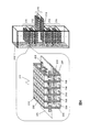
- FIG. 6 illustrates a configuration diagram of a server using the optical connector according to the present embodiment and an enlarged view of a unit substrate that configures the server.
- FIG. 6 shows a diagram in which unit boards 211, 212, 213, 214, 215, and 216 are mounted on the rack 210.
- the unit substrate is mounted with a large number of electronic components 208 such as a CPU / memory controller on the back surface as well as the front surface.
- electronic components 208 such as a CPU / memory controller
- the electrical signal from each electronic component 208 is converted into an optical signal via an optical module (not shown), and is output from the optical fiber outlet of the receptacle 202 in the connector member 201 through the optical fiber.
- the light is output from the outlet of the optical fiber of the receptacle 204 in the connector member 205 in the same manner as the front surface.
- the connector member is provided with a control lever 206 for each connector so that the receptacle can move up and down for connection with other connectors.
- FIG. 6 shows how the unit substrate 213 is inserted and removed.
- the connector of the unit substrate 213 and the connector of the unit substrate 214 are connected.
- the wiring of the electronic components on the unit substrate 213 and the electronic components on the unit substrate 214 is completed.
- the control lever 206 is turned off on the unit board 213 in the rack, the connector of the unit board 213 and the connector of the unit board 214 are disconnected.
- the unit substrate 213 can be pulled out.
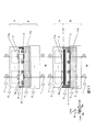
- FIG. 7 shows a configuration diagram of a server using the optical connector device according to the present embodiment, and an enlarged view of a unit board constituting the server.
- FIG. 7 shows a diagram in which unit boards 221, 222, 223, 224, 225, and 226 are mounted on the rack 210.
- the unit substrate is mounted with a large number of electronic components 208 such as a CPU / memory controller on the back surface as well as the front surface.
- electronic components 208 such as a CPU / memory controller
- the electrical signal from each electronic component 208 is converted into an optical signal through an optical module (not shown), and is output from the receptacle 202 in the connector member 201 through the optical fiber.
- the receptacle 204 in the connector member 205 in the same manner as the front surface.
- the connector is provided with a control lever 209 so that all receptacles can be moved up and down collectively for connection with other connectors.
- FIG. 7 shows how the unit substrate 223 is inserted and removed.
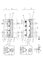
- FIG. 8A and 8B are configuration diagrams of the optical connector device according to the present embodiment, in which FIG. 8A shows a connector connection state and FIG. 8B shows a connector disconnection state.
- FIG. 9 is an enlarged view of the alignment mark portion of FIG. 8, where (a) shows a connection state between the magnet and the magnetic material, and (b) shows a separation state between the magnet and the magnetic material.
- the connector member A and the connector member B are kept connected by the magnet mechanism, and the connector member A and the connector member B are held by the magnetic shielding means as shown in FIG. 8B. Is cut off.
- FIG. 9 illustrates the details of the alignment mark shown in FIG. As shown in FIG. 9, the alignment mark is composed of a circular magnet and a wedge-shaped magnetic material.
- FIG. 9A when the straight line connecting the N pole and the S pole of the magnet is parallel to the magnetic material, the magnetic lines of force enter the magnetic material through the yoke 21.
- the suction force works between them, and they are in a state of sticking together.
- the contact surface is only a slope of a wedge-shaped magnetic material.
- FIG. 9B when the straight line connecting the north and south poles of the magnet is perpendicular to the magnetic material, the magnetic force lines cannot enter the magnetic material and the magnet and the magnetic material are separated. It becomes a state.
- FIG. 9 since the magnetic material has a wedge shape, the contact surface with the magnet is small, and the rotary magnet and the magnetic material can be easily separated. In this way, by manually rotating the magnet, the magnet and the magnetic material can be easily connected and disconnected.
- FIG. 8 illustrates a case where this mechanism is employed.
- FIG. 10A and 10B are configuration diagrams of the optical connector device according to the present embodiment, where FIG. 10A shows a connector connection state, and FIG. 10B shows a connector disconnection state.
- the connector member A is provided with an opening for inserting a shielding plate.
- the magnetic material 3 of the connector member A can freely move in the direction of the arrow shown in FIG.
- the alignment mark is composed of the magnet 4 and the magnetic material 3, the magnet has a circular shape, and the surface of the magnetic material facing the magnet has a wedge shape. Therefore, the contact surface between the magnet and the magnetic material is a wedge-shaped slope as shown in FIG.
- the connector member A and the connector member B are kept connected by the magnet mechanism by an attractive force on the contact surface between the magnetic material and the magnet.
- the connector member A and the connector member B are separated by inserting a shielding plate into the connector 1 housing opening, as shown in FIG.
- the attractive force that holds the connection is only the contact surface between the magnet and the magnetic material, and can be easily separated.
- FIGS. 11A and 11B are configuration diagrams of the optical connector device according to the present embodiment, in which FIG. 11A shows a connector connected state, and FIG. 11B shows a connector disconnected state.
- the connector member A is provided with an opening for inserting a shielding plate.
- the magnetic material 3 of the connector member A can freely move in the direction of the arrow shown in FIG.
- the alignment mark is composed of the magnet 4 and the magnetic material 3, and the magnet has a circular shape, and the surface of the magnetic material facing the magnet has an area larger than that of the opposite surface. It has a small shape. Therefore, the contact surface between the magnet and the magnetic material is an upper surface having a small trapezoidal area.
- the connector member A and the connector member B are kept connected by the magnet mechanism by an attractive force on the contact surface between the magnetic material and the magnet.
- the connector member A and the connector member B are separated by inserting a shielding plate into the opening of the connector member A as shown in FIG.
- the attractive force holding the connection is only a slight contact surface between the magnet and the magnetic material, and can be easily separated.
- FIGS. 12A and 12B are configuration diagrams of the optical connector device according to the present embodiment, where FIG. 12A shows a connector connection state and FIG. 12B shows a connector disconnection state.
- the connector housing and the connector housing B have a structure that does not come into contact with the protrusion 8.
- the connection state between the connector member A and the connector member B is held by the attractive force of the magnet 3 and the magnetic material 4.
- the magnet N pole or S pole 12 on the side wall of the connector member A exerts a repulsive force on the connector member A against the connector member B by the magnet N pole or S pole 13 on the side wall of the connector 2.
- the connection state between the connector 1 and the connector 2 becomes stronger and a connector connection structure that is resistant to external vibrations is obtained.
- FIGS. 13A and 13B are configuration diagrams of the optical connector device according to the present embodiment, where FIG. 13A shows a connector connection state, and FIG. 13B shows a connector disconnection state.
- the connector member A and the connector member B have a structure that does not come into contact with the protrusion 8.
- the connection state between the connector member A and the connector member B is held by the attractive force of the magnet 3 and the magnetic material 4.
- the magnet 9 of the connector member B has an N pole on the inside and an S pole on the outside
- a repulsive force acts between the magnet 9 and the magnet 3 due to the N pole on the tip side of the magnet 3 in the connector 2.
- the magnet 9 of the connector B has an S pole on the inner side and an N pole on the outer side
- a repulsive force is generated between the magnet 9 and the magnet 3 by the S pole on the tip side of the magnet 3 in the connector member 2. Due to this repulsive force, the connector member A has a structure that is difficult to be displaced laterally with respect to the connector member B, so that the connection state between the connector member A and the connector member B becomes stronger and is resistant to external vibration. It becomes.
- FIG. 14A and 14B are configuration diagrams of the optical connector device according to the present embodiment, in which FIG. 14A shows a connector connected state, and FIG. 14B shows a connector disconnected state.
- connection state of the connector member A and the connector member B is held by the attractive force of the electromagnet 4 and the magnetic material 3.
- the electromagnet 4 can control the timing of the attractive force generation between the electromagnet 4 and the magnetic material 3 by an external electric signal. Therefore, the connection / disconnection state of the connector member A and the connector member B can be controlled by an external operation from a long distance.
- FIGS. 15A and 15B are configuration diagrams of the optical connector device according to the present embodiment, where FIG. 15A shows a connector connected state, and FIG. 15B shows a connector disconnected state.
- the connector member A and the connector member B have a structure that does not come into contact with the protrusion 8.
- the connection state of the connector member A and the connector member B is held by the attractive force between the magnet 4 and the magnetic material 3 that are alignment marks.
- FIGS. 16A and 16B are configuration diagrams of the optical connector device according to the present embodiment, where FIG. 16A shows a connector connection state and FIG. 16B shows a connector disconnection state.
- the connector member A and the connector member B have a structure that does not come into contact with the protrusion 8.
- the connection state between the connector member A and the connector member B is held by the attractive force of the magnet 4 and the magnetic material 3.
- the connector member B has a rail structure 20 into which a plate-shaped member can be inserted.
- the connection state between the connector member A and the connector member B In FIG. 16A, a shield plate is interposed between the magnet 4 and the magnetic material 3 using the shield plate and the rail structure 20 that weaken the magnetic force. By inserting, the connector member A and the connector member B can be separated, and the connection between the connector member A and the connector member B is turned off.
- FIG. 16B shows a connection-off state between the connector member A and the connector member B.
- FIGS. 17A and 17B are configuration diagrams of the optical connector device according to the present embodiment, in which FIG. 17A shows a connector connected state, and FIG. 17B shows a connector disconnected state.
- the connector member A and the connector member B have a structure that does not come into contact with the protrusion 8.
- the connection state of the connector member A and the connector member B is held by the attractive force of the N pole or S pole of the magnet 4 and the S pole or N pole of the magnet 3a.
- the connector member B has a rail structure 20 into which a plate-shaped member can be inserted.
- the connection state of the connector member A and the connector member B In FIG. 16A, the shielding plate is inserted between the magnet 4 and the magnetic material 3 using the plate-like magnet and the rail structure 20.
- the magnet 3a is an N pole and the magnet 4 is an S pole
- the upper side of the plate-shaped magnet is the N pole and the lower side is the S pole.
- the magnet 3a is the S pole and the magnet 4 is the N pole
- the upper side of the plate-shaped magnet is the S pole and the lower side is the N pole.
- the optical connector is configured to transmit and receive signals between the board and another board.
- the present invention is not limited to this mode, and a plurality of optical connectors are used.
- the present invention can be applied to any optical connector device or an optical connector for signal transmission / reception other than between the substrates described above.
Landscapes
- Physics & Mathematics (AREA)
- General Physics & Mathematics (AREA)
- Optics & Photonics (AREA)
- Optical Couplings Of Light Guides (AREA)
Priority Applications (1)
| Application Number | Priority Date | Filing Date | Title |
|---|---|---|---|
| PCT/JP2012/067641 WO2014010035A1 (fr) | 2012-07-11 | 2012-07-11 | Connecteur optique et serveur utilisant un connecteur optique |
Applications Claiming Priority (1)
| Application Number | Priority Date | Filing Date | Title |
|---|---|---|---|
| PCT/JP2012/067641 WO2014010035A1 (fr) | 2012-07-11 | 2012-07-11 | Connecteur optique et serveur utilisant un connecteur optique |
Publications (1)
| Publication Number | Publication Date |
|---|---|
| WO2014010035A1 true WO2014010035A1 (fr) | 2014-01-16 |
Family
ID=49915538
Family Applications (1)
| Application Number | Title | Priority Date | Filing Date |
|---|---|---|---|
| PCT/JP2012/067641 Ceased WO2014010035A1 (fr) | 2012-07-11 | 2012-07-11 | Connecteur optique et serveur utilisant un connecteur optique |
Country Status (1)
| Country | Link |
|---|---|
| WO (1) | WO2014010035A1 (fr) |
Cited By (2)
| Publication number | Priority date | Publication date | Assignee | Title |
|---|---|---|---|---|
| JPWO2022153354A1 (fr) * | 2021-01-12 | 2022-07-21 | ||
| EP3230778B1 (fr) * | 2014-12-14 | 2023-10-25 | Telescent Inc. | Systèmes de connexion transversale robotique à fiabilité élevée |
Citations (7)
| Publication number | Priority date | Publication date | Assignee | Title |
|---|---|---|---|---|
| JPH0173774U (fr) * | 1987-11-06 | 1989-05-18 | ||
| JPH04286882A (ja) * | 1991-03-18 | 1992-10-12 | Toyota Autom Loom Works Ltd | バッテリ式フォークリフトのバッテリコネクタ装置 |
| JPH10255894A (ja) * | 1997-03-11 | 1998-09-25 | Sumitomo Electric Ind Ltd | 電磁着脱コネクタ |
| JP2005045490A (ja) * | 2003-07-28 | 2005-02-17 | Kyocera Corp | 携帯端末機器のコネクタ構造 |
| JP2006515102A (ja) * | 2002-09-13 | 2006-05-18 | マグコード アーゲー | 電気接続装置 |
| JP2009510674A (ja) * | 2005-09-26 | 2009-03-12 | アップル インコーポレイテッド | 電子装置の電磁コネクタ |
| JP2011520151A (ja) * | 2008-05-09 | 2011-07-14 | ヒューレット−パッカード デベロップメント カンパニー エル.ピー. | 近接自由空間光インターコネクト |
-
2012
- 2012-07-11 WO PCT/JP2012/067641 patent/WO2014010035A1/fr not_active Ceased
Patent Citations (7)
| Publication number | Priority date | Publication date | Assignee | Title |
|---|---|---|---|---|
| JPH0173774U (fr) * | 1987-11-06 | 1989-05-18 | ||
| JPH04286882A (ja) * | 1991-03-18 | 1992-10-12 | Toyota Autom Loom Works Ltd | バッテリ式フォークリフトのバッテリコネクタ装置 |
| JPH10255894A (ja) * | 1997-03-11 | 1998-09-25 | Sumitomo Electric Ind Ltd | 電磁着脱コネクタ |
| JP2006515102A (ja) * | 2002-09-13 | 2006-05-18 | マグコード アーゲー | 電気接続装置 |
| JP2005045490A (ja) * | 2003-07-28 | 2005-02-17 | Kyocera Corp | 携帯端末機器のコネクタ構造 |
| JP2009510674A (ja) * | 2005-09-26 | 2009-03-12 | アップル インコーポレイテッド | 電子装置の電磁コネクタ |
| JP2011520151A (ja) * | 2008-05-09 | 2011-07-14 | ヒューレット−パッカード デベロップメント カンパニー エル.ピー. | 近接自由空間光インターコネクト |
Cited By (7)
| Publication number | Priority date | Publication date | Assignee | Title |
|---|---|---|---|---|
| EP3230778B1 (fr) * | 2014-12-14 | 2023-10-25 | Telescent Inc. | Systèmes de connexion transversale robotique à fiabilité élevée |
| EP4336232A3 (fr) * | 2014-12-14 | 2024-06-26 | Telescent Inc. | Systèmes de connexion transversale robotique à haute fiabilité |
| JPWO2022153354A1 (fr) * | 2021-01-12 | 2022-07-21 | ||
| WO2022153354A1 (fr) * | 2021-01-12 | 2022-07-21 | 日本電信電話株式会社 | Structure de montage de module optique et carte de montage optique |
| CN116745669A (zh) * | 2021-01-12 | 2023-09-12 | 日本电信电话株式会社 | 光学模块的安装结构和光学安装板 |
| JP7556412B2 (ja) | 2021-01-12 | 2024-09-26 | 日本電信電話株式会社 | 光モジュールの実装構造および光実装ボード |
| CN116745669B (zh) * | 2021-01-12 | 2026-04-07 | 恩梯梯株式会社 | 光学模块的安装结构和光学安装板 |
Similar Documents
| Publication | Publication Date | Title |
|---|---|---|
| US11863917B2 (en) | Assembly of network switch ASIC with optical transceivers | |
| CN102307142B (zh) | 背板系统 | |
| US20140029888A1 (en) | Electro-optical assembly for silicon photonic chip and electro-optical carrier | |
| CN104067541B (zh) | 光物理接口模块 | |
| TWI529437B (zh) | 資料中心光學(dco)邊緣安裝收發器總成與其維修方法、以及插頭連接器 | |
| JP5608202B2 (ja) | コネクタハウジングと半導体サブモジュールとの接続方法 | |
| JP5445579B2 (ja) | 光導波路モジュール | |
| KR100570416B1 (ko) | 광 도파관 접속용의 계단 구조 제공 장치 및 광 도파관 형성 방법 | |
| EP3028083B1 (fr) | Module émetteur-récepteur optoélectrique et câble optique actif | |
| CN100566045C (zh) | 光电复合式连接器以及使用它的基板 | |
| Bamiedakis et al. | A 40 Gb/s optical bus for optical backplane interconnections | |
| JP2009003253A (ja) | 光電気混載基板と光電気パッケージとの構造体 | |
| US8867231B2 (en) | Electronic module packages and assemblies for electrical systems | |
| CN1715979A (zh) | 具有刚性和挠性电路板的光纤收发机模块 | |
| JP2010211179A (ja) | 光電気複合配線モジュールおよびその製造方法 | |
| WO2013046415A1 (fr) | Module optique | |
| Bamiedakis et al. | Low-cost PCB-integrated 10-Gb/s optical transceiver built with a novel integration method | |
| JP2009288614A (ja) | 平面型光導波路アレイモジュールとその製造方法 | |
| US20080080807A1 (en) | Opto-electronic connector module and opto-electronic communication module having the same | |
| WO2014010035A1 (fr) | Connecteur optique et serveur utilisant un connecteur optique | |
| US10120148B2 (en) | Devices with optical ports in fan-out configurations | |
| CN118265936A (zh) | 光模块 | |
| US8947796B2 (en) | Telecentric optical assembly | |
| CN116184579B (zh) | 一种光模块 | |
| Immonen et al. | Development of electro‐optical PCBs with polymer waveguides for high‐speed intra‐system interconnects |
Legal Events
| Date | Code | Title | Description |
|---|---|---|---|
| 121 | Ep: the epo has been informed by wipo that ep was designated in this application |
Ref document number: 12880945 Country of ref document: EP Kind code of ref document: A1 |
|
| NENP | Non-entry into the national phase |
Ref country code: DE |
|
| 122 | Ep: pct application non-entry in european phase |
Ref document number: 12880945 Country of ref document: EP Kind code of ref document: A1 |
|
| NENP | Non-entry into the national phase |
Ref country code: JP |