WO2014013574A1 - Convertisseur de puissance - Google Patents
Convertisseur de puissance Download PDFInfo
- Publication number
- WO2014013574A1 WO2014013574A1 PCT/JP2012/068239 JP2012068239W WO2014013574A1 WO 2014013574 A1 WO2014013574 A1 WO 2014013574A1 JP 2012068239 W JP2012068239 W JP 2012068239W WO 2014013574 A1 WO2014013574 A1 WO 2014013574A1
- Authority
- WO
- WIPO (PCT)
- Prior art keywords
- power converter
- voltage
- switches
- resonant
- resonance
- Prior art date
- Legal status (The legal status is an assumption and is not a legal conclusion. Google has not performed a legal analysis and makes no representation as to the accuracy of the status listed.)
- Ceased
Links
Images

Classifications
-
- H—ELECTRICITY
- H02—GENERATION; CONVERSION OR DISTRIBUTION OF ELECTRIC POWER
- H02M—APPARATUS FOR CONVERSION BETWEEN AC AND AC, BETWEEN AC AND DC, OR BETWEEN DC AND DC, AND FOR USE WITH MAINS OR SIMILAR POWER SUPPLY SYSTEMS; CONVERSION OF DC OR AC INPUT POWER INTO SURGE OUTPUT POWER; CONTROL OR REGULATION THEREOF
- H02M5/00—Conversion of AC power input into AC power output, e.g. for change of voltage, for change of frequency, for change of number of phases
- H02M5/40—Conversion of AC power input into AC power output, e.g. for change of voltage, for change of frequency, for change of number of phases with intermediate conversion into DC
- H02M5/42—Conversion of AC power input into AC power output, e.g. for change of voltage, for change of frequency, for change of number of phases with intermediate conversion into DC by static converters
- H02M5/44—Conversion of AC power input into AC power output, e.g. for change of voltage, for change of frequency, for change of number of phases with intermediate conversion into DC by static converters using discharge tubes or semiconductor devices to convert the intermediate DC into AC
- H02M5/453—Conversion of AC power input into AC power output, e.g. for change of voltage, for change of frequency, for change of number of phases with intermediate conversion into DC by static converters using discharge tubes or semiconductor devices to convert the intermediate DC into AC using devices of a triode or transistor type requiring continuous application of a control signal
- H02M5/458—Conversion of AC power input into AC power output, e.g. for change of voltage, for change of frequency, for change of number of phases with intermediate conversion into DC by static converters using discharge tubes or semiconductor devices to convert the intermediate DC into AC using devices of a triode or transistor type requiring continuous application of a control signal using semiconductor devices only
-
- H—ELECTRICITY
- H02—GENERATION; CONVERSION OR DISTRIBUTION OF ELECTRIC POWER
- H02M—APPARATUS FOR CONVERSION BETWEEN AC AND AC, BETWEEN AC AND DC, OR BETWEEN DC AND DC, AND FOR USE WITH MAINS OR SIMILAR POWER SUPPLY SYSTEMS; CONVERSION OF DC OR AC INPUT POWER INTO SURGE OUTPUT POWER; CONTROL OR REGULATION THEREOF
- H02M1/00—Details of apparatus for conversion
- H02M1/40—Means for preventing magnetic saturation
-
- H—ELECTRICITY
- H02—GENERATION; CONVERSION OR DISTRIBUTION OF ELECTRIC POWER
- H02M—APPARATUS FOR CONVERSION BETWEEN AC AND AC, BETWEEN AC AND DC, OR BETWEEN DC AND DC, AND FOR USE WITH MAINS OR SIMILAR POWER SUPPLY SYSTEMS; CONVERSION OF DC OR AC INPUT POWER INTO SURGE OUTPUT POWER; CONTROL OR REGULATION THEREOF
- H02M7/00—Conversion of AC power input into DC power output; Conversion of DC power input into AC power output
- H02M7/42—Conversion of DC power input into AC power output without possibility of reversal
- H02M7/44—Conversion of DC power input into AC power output without possibility of reversal by static converters
- H02M7/48—Conversion of DC power input into AC power output without possibility of reversal by static converters using discharge tubes with control electrode or semiconductor devices with control electrode
- H02M7/53—Conversion of DC power input into AC power output without possibility of reversal by static converters using discharge tubes with control electrode or semiconductor devices with control electrode using devices of a triode or transistor type requiring continuous application of a control signal
- H02M7/537—Conversion of DC power input into AC power output without possibility of reversal by static converters using discharge tubes with control electrode or semiconductor devices with control electrode using devices of a triode or transistor type requiring continuous application of a control signal using semiconductor devices only, e.g. single switched pulse inverters
- H02M7/538—Conversion of DC power input into AC power output without possibility of reversal by static converters using discharge tubes with control electrode or semiconductor devices with control electrode using devices of a triode or transistor type requiring continuous application of a control signal using semiconductor devices only, e.g. single switched pulse inverters in a push-pull configuration
-
- H—ELECTRICITY
- H02—GENERATION; CONVERSION OR DISTRIBUTION OF ELECTRIC POWER
- H02M—APPARATUS FOR CONVERSION BETWEEN AC AND AC, BETWEEN AC AND DC, OR BETWEEN DC AND DC, AND FOR USE WITH MAINS OR SIMILAR POWER SUPPLY SYSTEMS; CONVERSION OF DC OR AC INPUT POWER INTO SURGE OUTPUT POWER; CONTROL OR REGULATION THEREOF
- H02M7/00—Conversion of AC power input into DC power output; Conversion of DC power input into AC power output
- H02M7/42—Conversion of DC power input into AC power output without possibility of reversal
- H02M7/44—Conversion of DC power input into AC power output without possibility of reversal by static converters
- H02M7/48—Conversion of DC power input into AC power output without possibility of reversal by static converters using discharge tubes with control electrode or semiconductor devices with control electrode
- H02M7/4803—Conversion of DC power input into AC power output without possibility of reversal by static converters using discharge tubes with control electrode or semiconductor devices with control electrode with means for reducing DC component from AC output voltage
-
- H—ELECTRICITY
- H02—GENERATION; CONVERSION OR DISTRIBUTION OF ELECTRIC POWER
- H02M—APPARATUS FOR CONVERSION BETWEEN AC AND AC, BETWEEN AC AND DC, OR BETWEEN DC AND DC, AND FOR USE WITH MAINS OR SIMILAR POWER SUPPLY SYSTEMS; CONVERSION OF DC OR AC INPUT POWER INTO SURGE OUTPUT POWER; CONTROL OR REGULATION THEREOF
- H02M7/00—Conversion of AC power input into DC power output; Conversion of DC power input into AC power output
- H02M7/42—Conversion of DC power input into AC power output without possibility of reversal
- H02M7/44—Conversion of DC power input into AC power output without possibility of reversal by static converters
- H02M7/48—Conversion of DC power input into AC power output without possibility of reversal by static converters using discharge tubes with control electrode or semiconductor devices with control electrode
- H02M7/4807—Conversion of DC power input into AC power output without possibility of reversal by static converters using discharge tubes with control electrode or semiconductor devices with control electrode having a high frequency intermediate AC stage
-
- H—ELECTRICITY
- H02—GENERATION; CONVERSION OR DISTRIBUTION OF ELECTRIC POWER
- H02M—APPARATUS FOR CONVERSION BETWEEN AC AND AC, BETWEEN AC AND DC, OR BETWEEN DC AND DC, AND FOR USE WITH MAINS OR SIMILAR POWER SUPPLY SYSTEMS; CONVERSION OF DC OR AC INPUT POWER INTO SURGE OUTPUT POWER; CONTROL OR REGULATION THEREOF
- H02M7/00—Conversion of AC power input into DC power output; Conversion of DC power input into AC power output
- H02M7/42—Conversion of DC power input into AC power output without possibility of reversal
- H02M7/44—Conversion of DC power input into AC power output without possibility of reversal by static converters
- H02M7/48—Conversion of DC power input into AC power output without possibility of reversal by static converters using discharge tubes with control electrode or semiconductor devices with control electrode
- H02M7/4815—Resonant converters
-
- Y—GENERAL TAGGING OF NEW TECHNOLOGICAL DEVELOPMENTS; GENERAL TAGGING OF CROSS-SECTIONAL TECHNOLOGIES SPANNING OVER SEVERAL SECTIONS OF THE IPC; TECHNICAL SUBJECTS COVERED BY FORMER USPC CROSS-REFERENCE ART COLLECTIONS [XRACs] AND DIGESTS
- Y02—TECHNOLOGIES OR APPLICATIONS FOR MITIGATION OR ADAPTATION AGAINST CLIMATE CHANGE
- Y02B—CLIMATE CHANGE MITIGATION TECHNOLOGIES RELATED TO BUILDINGS, e.g. HOUSING, HOUSE APPLIANCES OR RELATED END-USER APPLICATIONS
- Y02B70/00—Technologies for an efficient end-user side electric power management and consumption
- Y02B70/10—Technologies improving the efficiency by using switched-mode power supplies [SMPS], i.e. efficient power electronics conversion e.g. power factor correction or reduction of losses in power supplies or efficient standby modes
Definitions
- This invention relates to a power converter.
- the switching power supply circuit disclosed in Patent Document 2 has a single transformer secondary winding, and two independent circuits each for half-wave rectifying the voltage induced in the secondary winding are provided. Suppresses the demagnetization.
- Patent Document 1 requires a memory circuit that stores the current polarity when an overcurrent occurs, and the switching power supply circuit disclosed in Patent Document 2 is an independent circuit that performs half-wave rectification on the secondary side.
- the circuit becomes complicated.
- the present invention has been made in view of the above-described circumstances, and an object thereof is to prevent biasing of a transformer with a simple configuration.
- a power converter is a power converter that includes a resonant transformer having a primary winding and a secondary winding, converts an input DC voltage into an AC voltage, and outputs the AC voltage. It includes two resonant capacitors, two switches, and a control unit. The two resonant capacitors are connected in series, and a divided DC voltage is applied to each. The two switches are connected to the primary winding of the resonant transformer and the corresponding resonant capacitor of the two resonant capacitors, and when one of the switches is in the ON state, the terminal of the connected resonant capacitor A voltage is applied to the primary winding of the resonant transformer based on the inter-voltage.
- the control unit When starting the drive of the power converter, the control unit outputs a gate signal for turning on one of the determined switches for a predetermined conduction time, and then the switches are alternately turned on for the conduction time.
- the gate signal is output so that the power converter is stopped, when the drive is started after the switch that has not been turned on when the drive is started is turned on for the conduction time.
- the gate signal is output so that the two switches are in the off state without the switch in the on state being in the on state.
- the transformer it is possible to prevent the transformer from being demagnetized with a simple configuration.
- FIG. 1 It is a block diagram which shows the structural example of a power converter device provided with the power converter which concerns on embodiment of this invention. It is a figure which shows the example of the change of the voltage of the resonant capacitor and resonant transformer in embodiment.
- FIG. 1 is a block diagram illustrating a configuration example of a power conversion device including a power converter according to an embodiment of the present invention.
- the power conversion device includes a power converter 1, a power source 3, a rectifier circuit 4, a smoothing capacitor C 1, and a secondary circuit 5.
- the AC voltage output from the power supply 3 is converted into DC by the rectifier circuit 4, smoothed by the smoothing capacitor C ⁇ b> 1, and supplied to the power converter 1.
- the power converter 1 converts the input DC voltage into an AC voltage and outputs the AC voltage to the secondary circuit 5.
- the secondary circuit 5 may convert the alternating current into direct current and output it, or may output the alternating current as it is.
- the power source 3 may be a DC power source, and may be configured to include a coil connected to the positive side of the power source 3 and the smoothing capacitor C1 instead of the rectifier circuit 4.
- the power converter 1 includes resonant capacitors C2 and C3, switches SW1 and SW2, a resonant transformer TR, and a control unit 2.
- the resonant capacitors C2 and C3 are connected in series. Before the power converter 1 starts to be driven, the divided DC voltage is applied to the resonance capacitors C2 and C3, respectively.
- the capacitances of the resonance capacitors C2 and C3 may be the same value or different values. When the capacitances of the resonance capacitors C2 and C3 are the same, the voltage values of the resonance capacitors C2 and C3 are the same.
- the resonant capacitors C2 and C3 may be composed of a plurality of capacitors connected in series and / or a plurality of capacitors connected in parallel. In that case, the capacitances of the resonant capacitors C2 and C3 are the combined capacitances of a plurality of capacitors. Further, the switches SW1 and SW2 may be composed of a plurality of elements.
- the control unit 2 outputs a gate signal for switching the switches SW1 and SW2 on and off. For example, when the input voltage to the power converter 1 detected by an input voltage detector (not shown) falls within a predetermined range, the control unit 2 starts driving the power converter 1. For example, when the input voltage to the power converter 1 exceeds the threshold value and becomes an overvoltage, the control unit 2 stops the power converter 1. Further, for example, when the current flowing through the resonance transformer TR detected by an overcurrent detector (not shown) exceeds the threshold value and becomes an overcurrent, the power converter 1 is stopped.
- the switches SW1 and SW2 are IGBTs (Insulated Gate Bipolar Transistors), but the switches SW1 and SW2 are not limited to IGBTs, and may be controlled by gate signals.
- the switches SW1 and SW2 are connected in series and are connected in parallel to the resonance capacitors C2 and C3.
- the resonant transformer TR has a primary winding and a secondary winding, and both ends of the primary winding of the resonant transformer TR are connected to a connection point of the resonance capacitors C2 and C3 and a connection point of the switches SW1 and SW2, respectively.
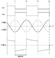
- FIG. 2 is a diagram illustrating an example of changes in voltages of the resonant capacitor and the resonant transformer in the embodiment.
- the operation of the power converter 1 will be described with reference to FIG.
- the capacitances of the resonant capacitors C2 and C3 are set to the same value, and when the control unit 2 starts driving the power converter 1, it outputs a gate signal that turns on the switch SW1 for a predetermined conduction time.
- the interval between alternate long and short dash lines is one conduction time of one switch (SW1 or SW2).
- the controller 2 outputs a gate signal so that the switches SW1 and SW2 are alternately turned on during the conduction time as shown in FIG.
- the short-circuit prevention time in which both the switches SW1 and SW2 are turned off is omitted.
- the change in voltage of the resonance capacitor C2 is indicated by a solid line
- the change in voltage of the resonance capacitor C3 is indicated by a dotted line.
- the switch SW1 is on and the switch SW2 is off
- the voltage of the resonance capacitor C2 decreases and the voltage of the resonance capacitor C3 increases.
- the switch SW1 is in the off state and the switch SW2 is in the on state
- the voltage of the resonance capacitor C2 increases and the voltage of the resonance capacitor C3 decreases.
- the sum of the voltage of the resonant capacitor C2 and the voltage of the resonant capacitor C3 is constant and matches the voltage input to the power converter 1.
- the capacitances of the resonant capacitors C2 and C3 are the same, assuming that the voltage input to the power converter 1 is V, the voltages of the resonant capacitors C2 and C3 change around 1 ⁇ 2V.
- the waveforms of the voltages of the resonant capacitors C2 and C3 are waveforms that are 180 degrees out of phase as shown in FIG.
- the current of the resonance transformer TR has a different polarity for each conduction time and has the same amplitude change. Therefore, as shown in FIG. 2, the primary winding of the resonant transformer TR is applied with a voltage having a different polarity for each conduction time and the same change in amplitude.
- the overcurrent detector detects an overcurrent.
- the power converter 1 is stopped immediately after the overcurrent is detected, or the time T3 after the lapse of the conduction time from the time T2 when the switch SW1 that is on when the overcurrent is detected is turned on. The power converter 1 was stopped.
- the voltage of the resonance capacitor C3 is in a state larger than the voltage of the resonance capacitor C2.
- the capacitances of the resonant capacitors C2 and C3 must be set to a relatively large value of several ⁇ F to several tens of ⁇ F. It takes a few minutes to discharge.
- the power converter 1 is required to start driving again immediately after being stopped due to detection of overvoltage or overcurrent, when the power converter 1 is stopped at time T3, the resonant capacitor is started when driving is started.
- the voltage of C3 is larger than the voltage of the resonant capacitor C2.
- the resonance capacitor C3 is further charged. Therefore, the voltage of the resonance capacitor C3 changes centering on a value larger than 1 / 2V, and the voltage of the resonance capacitor C2 changes centering on a value smaller than 1 / 2V.
- the magnetic flux density applied to the primary winding of the resonance transformer TR is a value obtained by multiplying the voltage applied to the primary winding of the resonance transformer TR by the conduction time.
- the switch SW1 is turned on during the conduction time, so that the resonance transformer TR The magnetic flux density applied to the primary winding is canceled by turning on the switch SW2 during the conduction time. Therefore, when the switches SW1 and SW2 are on during the conduction time while the power converter 1 is being driven, the resonance transformer TR is not demagnetized.
- the power converter 1 when the power converter 1 is started after the power converter 1 is stopped at the time T3 and the switch SW1 is turned on, the voltage applied to the primary winding of the resonance transformer TR. Becomes a different value for each conduction time, and the resonance transformer TR is demagnetized.
- the control unit 2 when starting the driving of the power converter 1, the control unit 2 outputs a gate signal that turns on the switch SW1 for a predetermined conduction time.
- the switch SW ⁇ b> 2 that has not been turned on when driving is turned on for the conduction time and then turned on when driving is started.
- the gate signal is output so that the switches SW1 and SW2 are turned off without the switch SW1 turned on. That is, when an overcurrent is detected between time T2 and T3, the control unit 2 turns off the switches SW1 and SW2 at time T4 immediately after the switch SW2 is turned on for the conduction time.
- the gate signal is output as follows. When the power converter 1 is stopped at time T4, the voltage of the resonance capacitor C2 is larger than the voltage of the resonance capacitor C3.
- the control unit 2 outputs a gate signal for turning on the switch SW1 during the conduction time, so that the resonance capacitor C3 is charged, and the voltages of the resonance capacitors C2 and C3 are As shown in FIG.
- the voltage applied to the primary winding of the resonant transformer TR has a different polarity for each conduction time and the same amplitude change, so that the resonant transformer TR is not demagnetized.
- the control unit 2 when the drive of the power converter 1 is started, the control unit 2 outputs a gate signal so that any one of the switches SW1 and SW2 is turned on.
- a switch SW1 or SW2
- the control unit 2 may output a gate signal that turns on the switch SW2.
- the capacitances of the resonant capacitors C2 and C3 are different, the average value of the maximum value and the minimum value of the voltages of the resonant capacitors C2 and C3 is different, but at any time, the voltage of the resonant capacitor C2 and the voltage of the resonant capacitor C3 are different.
- the total is constant and matches the voltage input to the power converter 1.
- the current of the resonance transformer TR has a different polarity for each conduction time and has the same amplitude change. Therefore, the voltage applied to the primary winding of the resonant transformer TR is a voltage that has a different polarity for each conduction time and has the same change in amplitude. Even when the capacitances of the resonant capacitors C2 and C3 are different, it is possible to suppress the bias of the resonant transformer TR by switching the switches SW1 and SW2 on and off as described above.
- the power converter 1 According to the power converter 1 according to the present embodiment, it is possible to prevent the bias of the resonant transformer TR with a simple configuration.
- a switch element formed of a wide band gap semiconductor having a larger band gap than silicon may be used for the switches SW1 and SW2.
- the wide band gap semiconductor is, for example, silicon carbide, a gallium nitride material, or diamond.
- a switching element formed of a wide band gap semiconductor has high withstand voltage and allowable current density. Therefore, the switching element can be miniaturized, and the semiconductor module incorporating the switching element can be miniaturized by using the miniaturized switching element.
- the wide band gap semiconductor has high heat resistance, it is possible to reduce the size of the heat sink fins and the air cooling of the water-cooled part, thereby further reducing the size of the semiconductor module. Furthermore, since the power loss is low, it is possible to increase the efficiency of the switching element, and consequently to increase the efficiency of the semiconductor module.
- the embodiment of the present invention is not limited to the above-described embodiment.
- the circuit configuration of the power converter 1 is not limited to the circuit of FIG. Connected in series to the primary windings of the two resonant capacitors C2, C3 and the resonant transformer TR to which the divided input voltage is applied, respectively, and the corresponding resonant capacitor C2 or resonant capacitor C3, If one of the switches is in the on state, two switches SW1 and SW2 for applying a voltage to the primary winding of the resonance transformer TR based on the voltage between the terminals of the resonance capacitor C2 or the resonance capacitor C3 to be connected are provided. Other circuit configurations may be used.
- the present invention can be suitably employed in a power converter that converts an input DC voltage into an AC voltage and outputs the AC voltage.
Landscapes
- Engineering & Computer Science (AREA)
- Power Engineering (AREA)
- Dc-Dc Converters (AREA)
Abstract
Priority Applications (4)
| Application Number | Priority Date | Filing Date | Title |
|---|---|---|---|
| PCT/JP2012/068239 WO2014013574A1 (fr) | 2012-07-18 | 2012-07-18 | Convertisseur de puissance |
| US14/414,738 US20150194903A1 (en) | 2012-07-18 | 2012-07-18 | Power converter |
| EP12881394.6A EP2876804A4 (fr) | 2012-07-18 | 2012-07-18 | Convertisseur de puissance |
| JP2014525607A JP5769886B2 (ja) | 2012-07-18 | 2012-07-18 | 電力変換器 |
Applications Claiming Priority (1)
| Application Number | Priority Date | Filing Date | Title |
|---|---|---|---|
| PCT/JP2012/068239 WO2014013574A1 (fr) | 2012-07-18 | 2012-07-18 | Convertisseur de puissance |
Publications (1)
| Publication Number | Publication Date |
|---|---|
| WO2014013574A1 true WO2014013574A1 (fr) | 2014-01-23 |
Family
ID=49948429
Family Applications (1)
| Application Number | Title | Priority Date | Filing Date |
|---|---|---|---|
| PCT/JP2012/068239 Ceased WO2014013574A1 (fr) | 2012-07-18 | 2012-07-18 | Convertisseur de puissance |
Country Status (4)
| Country | Link |
|---|---|
| US (1) | US20150194903A1 (fr) |
| EP (1) | EP2876804A4 (fr) |
| JP (1) | JP5769886B2 (fr) |
| WO (1) | WO2014013574A1 (fr) |
Families Citing this family (2)
| Publication number | Priority date | Publication date | Assignee | Title |
|---|---|---|---|---|
| EP4029139A4 (fr) | 2019-09-13 | 2023-09-27 | Milwaukee Electric Tool Corporation | Convertisseurs de puissance à semi-conducteurs à large bande interdite |
| US11726130B2 (en) * | 2020-08-26 | 2023-08-15 | Eaton Intelligent Power Limited | Hybrid switch for substation and other applications and methods of operating same |
Citations (8)
| Publication number | Priority date | Publication date | Assignee | Title |
|---|---|---|---|---|
| JPS5975324A (ja) * | 1982-10-22 | 1984-04-28 | Hitachi Ltd | スイツチング電源 |
| JPH0236769A (ja) | 1988-07-26 | 1990-02-06 | Shinko Electric Co Ltd | トランスの飽和リセット方法 |
| JPH0417567A (ja) | 1990-05-10 | 1992-01-22 | Koufu Nippon Denki Kk | スイッチング電源回路 |
| JPH04285476A (ja) * | 1991-03-15 | 1992-10-09 | Toshiba Corp | 電力変換装置 |
| JPH0523791U (ja) * | 1991-08-28 | 1993-03-26 | 株式会社三社電機製作所 | 絶縁型コンバータ装置 |
| JPH0745361A (ja) * | 1993-07-28 | 1995-02-14 | Matsushita Electric Ind Co Ltd | 高周波加熱装置 |
| JP2000278954A (ja) * | 1999-03-23 | 2000-10-06 | Mitsubishi Electric Corp | 電力変換装置 |
| JP2007194006A (ja) * | 2006-01-18 | 2007-08-02 | Hitachi Appliances Inc | 誘導加熱装置 |
Family Cites Families (10)
| Publication number | Priority date | Publication date | Assignee | Title |
|---|---|---|---|---|
| US4030019A (en) * | 1975-11-10 | 1977-06-14 | General Electric Company | Static inverter control circuit |
| KR100342457B1 (ko) * | 1994-02-10 | 2002-11-02 | 코닌클리케 필립스 일렉트로닉스 엔.브이. | 역률보정을하는고주파ac/ac컨버터 |
| TWI221053B (en) * | 2003-05-07 | 2004-09-11 | Uis Abler Electronics Co Ltd | Bi-directional dc/dc power converter with a neutral point |
| US7428159B2 (en) * | 2005-03-31 | 2008-09-23 | Silicon Laboratories Inc. | Digital PWM controller |
| US7135740B2 (en) * | 2004-09-27 | 2006-11-14 | Teledyne Licensing, Llc | High voltage FET switch with conductivity modulation |
| WO2008041399A1 (fr) * | 2006-10-02 | 2008-04-10 | Murata Manufacturing Co., Ltd. | Convertisseur cc-cc d'isolation à double extrémité |
| US7961482B2 (en) * | 2007-05-09 | 2011-06-14 | International Rectifier Corporation | Bi-directional HEMT/GaN half-bridge circuit |
| US7660136B2 (en) * | 2007-10-09 | 2010-02-09 | System General Corporation | Method and apparatus for synchronous rectifying of soft switching power converters |
| WO2012046534A1 (fr) * | 2010-10-06 | 2012-04-12 | 三菱電機株式会社 | Dispositif d'alimentation électrique |
| US9143043B2 (en) * | 2012-03-01 | 2015-09-22 | Infineon Technologies Ag | Multi-mode operation and control of a resonant converter |
-
2012
- 2012-07-18 JP JP2014525607A patent/JP5769886B2/ja active Active
- 2012-07-18 WO PCT/JP2012/068239 patent/WO2014013574A1/fr not_active Ceased
- 2012-07-18 EP EP12881394.6A patent/EP2876804A4/fr not_active Withdrawn
- 2012-07-18 US US14/414,738 patent/US20150194903A1/en not_active Abandoned
Patent Citations (8)
| Publication number | Priority date | Publication date | Assignee | Title |
|---|---|---|---|---|
| JPS5975324A (ja) * | 1982-10-22 | 1984-04-28 | Hitachi Ltd | スイツチング電源 |
| JPH0236769A (ja) | 1988-07-26 | 1990-02-06 | Shinko Electric Co Ltd | トランスの飽和リセット方法 |
| JPH0417567A (ja) | 1990-05-10 | 1992-01-22 | Koufu Nippon Denki Kk | スイッチング電源回路 |
| JPH04285476A (ja) * | 1991-03-15 | 1992-10-09 | Toshiba Corp | 電力変換装置 |
| JPH0523791U (ja) * | 1991-08-28 | 1993-03-26 | 株式会社三社電機製作所 | 絶縁型コンバータ装置 |
| JPH0745361A (ja) * | 1993-07-28 | 1995-02-14 | Matsushita Electric Ind Co Ltd | 高周波加熱装置 |
| JP2000278954A (ja) * | 1999-03-23 | 2000-10-06 | Mitsubishi Electric Corp | 電力変換装置 |
| JP2007194006A (ja) * | 2006-01-18 | 2007-08-02 | Hitachi Appliances Inc | 誘導加熱装置 |
Non-Patent Citations (1)
| Title |
|---|
| See also references of EP2876804A4 |
Also Published As
| Publication number | Publication date |
|---|---|
| EP2876804A1 (fr) | 2015-05-27 |
| JP5769886B2 (ja) | 2015-08-26 |
| EP2876804A4 (fr) | 2015-06-03 |
| JPWO2014013574A1 (ja) | 2016-06-30 |
| US20150194903A1 (en) | 2015-07-09 |
Similar Documents
| Publication | Publication Date | Title |
|---|---|---|
| US7778048B2 (en) | Switching power supply apparatus | |
| US9787204B2 (en) | Switching power supply device | |
| CN104956578B (zh) | 谐振转换器的启动期间的涌入电流控制 | |
| JP5552949B2 (ja) | アクティブクランプ型dcdcコンバータ | |
| JP6070853B2 (ja) | 絶縁ゲート型半導体装置 | |
| JP2004215371A (ja) | 電源回路 | |
| JP5910395B2 (ja) | ドライブ回路 | |
| US9312778B2 (en) | Power supply device | |
| JP6951631B2 (ja) | 同期整流回路及びスイッチング電源装置 | |
| TW202101890A (zh) | 功率轉換器及用於控制其之方法與控制器 | |
| KR20190016479A (ko) | Dc/dc 컨버터 | |
| CN104426379B (zh) | 变换器电路和用于运行这类变换器电路的方法 | |
| JP5516055B2 (ja) | 電力変換装置 | |
| JP5769886B2 (ja) | 電力変換器 | |
| JP5510846B2 (ja) | 共振型dcdcコンバータ | |
| JP5783597B2 (ja) | スイッチング電源装置 | |
| JP6485366B2 (ja) | 位相シフト方式フルブリッジ型電源回路 | |
| WO2015079565A1 (fr) | Dispositif d'alimentation électrique | |
| JP2022075146A (ja) | Dcdcコンバータ | |
| TWI814062B (zh) | 改良型llc諧振轉換裝置 | |
| KR101047339B1 (ko) | 전류 모드 제어기에서의 전류 검출 시스템 | |
| JP7220013B2 (ja) | 溶接電源装置 | |
| WO2010084588A1 (fr) | Circuit d'alimentation, amplificateur de puissance l'incorporant et montage de radiodiffusion | |
| JP5019819B2 (ja) | スイッチング電源装置 | |
| KR101024306B1 (ko) | 직류/직류 변환 장치 |
Legal Events
| Date | Code | Title | Description |
|---|---|---|---|
| 121 | Ep: the epo has been informed by wipo that ep was designated in this application |
Ref document number: 12881394 Country of ref document: EP Kind code of ref document: A1 |
|
| ENP | Entry into the national phase |
Ref document number: 2014525607 Country of ref document: JP Kind code of ref document: A |
|
| WWE | Wipo information: entry into national phase |
Ref document number: 14414738 Country of ref document: US |
|
| WWE | Wipo information: entry into national phase |
Ref document number: 2012881394 Country of ref document: EP |
|
| NENP | Non-entry into the national phase |
Ref country code: DE |