WO2014013773A1 - LINGOT DE MONOCRISTAL DE CARBURE DE SILICIUM (SiC) ET PROCÉDÉ DE PRODUCTION DE CE DERNIER - Google Patents
LINGOT DE MONOCRISTAL DE CARBURE DE SILICIUM (SiC) ET PROCÉDÉ DE PRODUCTION DE CE DERNIER Download PDFInfo
- Publication number
- WO2014013773A1 WO2014013773A1 PCT/JP2013/062955 JP2013062955W WO2014013773A1 WO 2014013773 A1 WO2014013773 A1 WO 2014013773A1 JP 2013062955 W JP2013062955 W JP 2013062955W WO 2014013773 A1 WO2014013773 A1 WO 2014013773A1
- Authority
- WO
- WIPO (PCT)
- Prior art keywords
- crystal
- solution
- growth
- sic single
- seed crystal
- Prior art date
- Legal status (The legal status is an assumption and is not a legal conclusion. Google has not performed a legal analysis and makes no representation as to the accuracy of the status listed.)
- Ceased
Links
Images








Classifications
-
- C—CHEMISTRY; METALLURGY
- C30—CRYSTAL GROWTH
- C30B—SINGLE-CRYSTAL GROWTH; UNIDIRECTIONAL SOLIDIFICATION OF EUTECTIC MATERIAL OR UNIDIRECTIONAL DEMIXING OF EUTECTOID MATERIAL; REFINING BY ZONE-MELTING OF MATERIAL; PRODUCTION OF A HOMOGENEOUS POLYCRYSTALLINE MATERIAL WITH DEFINED STRUCTURE; SINGLE CRYSTALS OR HOMOGENEOUS POLYCRYSTALLINE MATERIAL WITH DEFINED STRUCTURE; AFTER-TREATMENT OF SINGLE CRYSTALS OR A HOMOGENEOUS POLYCRYSTALLINE MATERIAL WITH DEFINED STRUCTURE; APPARATUS THEREFOR
- C30B19/00—Liquid-phase epitaxial-layer growth
- C30B19/10—Controlling or regulating
-
- C—CHEMISTRY; METALLURGY
- C30—CRYSTAL GROWTH
- C30B—SINGLE-CRYSTAL GROWTH; UNIDIRECTIONAL SOLIDIFICATION OF EUTECTIC MATERIAL OR UNIDIRECTIONAL DEMIXING OF EUTECTOID MATERIAL; REFINING BY ZONE-MELTING OF MATERIAL; PRODUCTION OF A HOMOGENEOUS POLYCRYSTALLINE MATERIAL WITH DEFINED STRUCTURE; SINGLE CRYSTALS OR HOMOGENEOUS POLYCRYSTALLINE MATERIAL WITH DEFINED STRUCTURE; AFTER-TREATMENT OF SINGLE CRYSTALS OR A HOMOGENEOUS POLYCRYSTALLINE MATERIAL WITH DEFINED STRUCTURE; APPARATUS THEREFOR
- C30B15/00—Single-crystal growth by pulling from a melt, e.g. Czochralski method
- C30B15/32—Seed holders, e.g. chucks
-
- C—CHEMISTRY; METALLURGY
- C30—CRYSTAL GROWTH
- C30B—SINGLE-CRYSTAL GROWTH; UNIDIRECTIONAL SOLIDIFICATION OF EUTECTIC MATERIAL OR UNIDIRECTIONAL DEMIXING OF EUTECTOID MATERIAL; REFINING BY ZONE-MELTING OF MATERIAL; PRODUCTION OF A HOMOGENEOUS POLYCRYSTALLINE MATERIAL WITH DEFINED STRUCTURE; SINGLE CRYSTALS OR HOMOGENEOUS POLYCRYSTALLINE MATERIAL WITH DEFINED STRUCTURE; AFTER-TREATMENT OF SINGLE CRYSTALS OR A HOMOGENEOUS POLYCRYSTALLINE MATERIAL WITH DEFINED STRUCTURE; APPARATUS THEREFOR
- C30B17/00—Single-crystal growth onto a seed which remains in the melt during growth, e.g. Nacken-Kyropoulos method
-
- C—CHEMISTRY; METALLURGY
- C30—CRYSTAL GROWTH
- C30B—SINGLE-CRYSTAL GROWTH; UNIDIRECTIONAL SOLIDIFICATION OF EUTECTIC MATERIAL OR UNIDIRECTIONAL DEMIXING OF EUTECTOID MATERIAL; REFINING BY ZONE-MELTING OF MATERIAL; PRODUCTION OF A HOMOGENEOUS POLYCRYSTALLINE MATERIAL WITH DEFINED STRUCTURE; SINGLE CRYSTALS OR HOMOGENEOUS POLYCRYSTALLINE MATERIAL WITH DEFINED STRUCTURE; AFTER-TREATMENT OF SINGLE CRYSTALS OR A HOMOGENEOUS POLYCRYSTALLINE MATERIAL WITH DEFINED STRUCTURE; APPARATUS THEREFOR
- C30B19/00—Liquid-phase epitaxial-layer growth
- C30B19/02—Liquid-phase epitaxial-layer growth using molten solvents, e.g. flux
- C30B19/04—Liquid-phase epitaxial-layer growth using molten solvents, e.g. flux the solvent being a component of the crystal composition
-
- C—CHEMISTRY; METALLURGY
- C30—CRYSTAL GROWTH
- C30B—SINGLE-CRYSTAL GROWTH; UNIDIRECTIONAL SOLIDIFICATION OF EUTECTIC MATERIAL OR UNIDIRECTIONAL DEMIXING OF EUTECTOID MATERIAL; REFINING BY ZONE-MELTING OF MATERIAL; PRODUCTION OF A HOMOGENEOUS POLYCRYSTALLINE MATERIAL WITH DEFINED STRUCTURE; SINGLE CRYSTALS OR HOMOGENEOUS POLYCRYSTALLINE MATERIAL WITH DEFINED STRUCTURE; AFTER-TREATMENT OF SINGLE CRYSTALS OR A HOMOGENEOUS POLYCRYSTALLINE MATERIAL WITH DEFINED STRUCTURE; APPARATUS THEREFOR
- C30B19/00—Liquid-phase epitaxial-layer growth
- C30B19/06—Reaction chambers; Boats for supporting the melt; Substrate holders
- C30B19/062—Vertical dipping system
-
- C—CHEMISTRY; METALLURGY
- C30—CRYSTAL GROWTH
- C30B—SINGLE-CRYSTAL GROWTH; UNIDIRECTIONAL SOLIDIFICATION OF EUTECTIC MATERIAL OR UNIDIRECTIONAL DEMIXING OF EUTECTOID MATERIAL; REFINING BY ZONE-MELTING OF MATERIAL; PRODUCTION OF A HOMOGENEOUS POLYCRYSTALLINE MATERIAL WITH DEFINED STRUCTURE; SINGLE CRYSTALS OR HOMOGENEOUS POLYCRYSTALLINE MATERIAL WITH DEFINED STRUCTURE; AFTER-TREATMENT OF SINGLE CRYSTALS OR A HOMOGENEOUS POLYCRYSTALLINE MATERIAL WITH DEFINED STRUCTURE; APPARATUS THEREFOR
- C30B19/00—Liquid-phase epitaxial-layer growth
- C30B19/06—Reaction chambers; Boats for supporting the melt; Substrate holders
- C30B19/068—Substrate holders
-
- C—CHEMISTRY; METALLURGY
- C30—CRYSTAL GROWTH
- C30B—SINGLE-CRYSTAL GROWTH; UNIDIRECTIONAL SOLIDIFICATION OF EUTECTIC MATERIAL OR UNIDIRECTIONAL DEMIXING OF EUTECTOID MATERIAL; REFINING BY ZONE-MELTING OF MATERIAL; PRODUCTION OF A HOMOGENEOUS POLYCRYSTALLINE MATERIAL WITH DEFINED STRUCTURE; SINGLE CRYSTALS OR HOMOGENEOUS POLYCRYSTALLINE MATERIAL WITH DEFINED STRUCTURE; AFTER-TREATMENT OF SINGLE CRYSTALS OR A HOMOGENEOUS POLYCRYSTALLINE MATERIAL WITH DEFINED STRUCTURE; APPARATUS THEREFOR
- C30B29/00—Single crystals or homogeneous polycrystalline material with defined structure characterised by the material or by their shape
- C30B29/10—Inorganic compounds or compositions
- C30B29/36—Carbides
-
- C—CHEMISTRY; METALLURGY
- C30—CRYSTAL GROWTH
- C30B—SINGLE-CRYSTAL GROWTH; UNIDIRECTIONAL SOLIDIFICATION OF EUTECTIC MATERIAL OR UNIDIRECTIONAL DEMIXING OF EUTECTOID MATERIAL; REFINING BY ZONE-MELTING OF MATERIAL; PRODUCTION OF A HOMOGENEOUS POLYCRYSTALLINE MATERIAL WITH DEFINED STRUCTURE; SINGLE CRYSTALS OR HOMOGENEOUS POLYCRYSTALLINE MATERIAL WITH DEFINED STRUCTURE; AFTER-TREATMENT OF SINGLE CRYSTALS OR A HOMOGENEOUS POLYCRYSTALLINE MATERIAL WITH DEFINED STRUCTURE; APPARATUS THEREFOR
- C30B9/00—Single-crystal growth from melt solutions using molten solvents
- C30B9/04—Single-crystal growth from melt solutions using molten solvents by cooling of the solution
- C30B9/06—Single-crystal growth from melt solutions using molten solvents by cooling of the solution using as solvent a component of the crystal composition
-
- Y—GENERAL TAGGING OF NEW TECHNOLOGICAL DEVELOPMENTS; GENERAL TAGGING OF CROSS-SECTIONAL TECHNOLOGIES SPANNING OVER SEVERAL SECTIONS OF THE IPC; TECHNICAL SUBJECTS COVERED BY FORMER USPC CROSS-REFERENCE ART COLLECTIONS [XRACs] AND DIGESTS
- Y10—TECHNICAL SUBJECTS COVERED BY FORMER USPC
- Y10T—TECHNICAL SUBJECTS COVERED BY FORMER US CLASSIFICATION
- Y10T117/00—Single-crystal, oriented-crystal, and epitaxy growth processes; non-coating apparatus therefor
- Y10T117/10—Apparatus
- Y10T117/1004—Apparatus with means for measuring, testing, or sensing
- Y10T117/1008—Apparatus with means for measuring, testing, or sensing with responsive control means
-
- Y—GENERAL TAGGING OF NEW TECHNOLOGICAL DEVELOPMENTS; GENERAL TAGGING OF CROSS-SECTIONAL TECHNOLOGIES SPANNING OVER SEVERAL SECTIONS OF THE IPC; TECHNICAL SUBJECTS COVERED BY FORMER USPC CROSS-REFERENCE ART COLLECTIONS [XRACs] AND DIGESTS
- Y10—TECHNICAL SUBJECTS COVERED BY FORMER USPC
- Y10T—TECHNICAL SUBJECTS COVERED BY FORMER US CLASSIFICATION
- Y10T428/00—Stock material or miscellaneous articles
- Y10T428/21—Circular sheet or circular blank
-
- Y—GENERAL TAGGING OF NEW TECHNOLOGICAL DEVELOPMENTS; GENERAL TAGGING OF CROSS-SECTIONAL TECHNOLOGIES SPANNING OVER SEVERAL SECTIONS OF THE IPC; TECHNICAL SUBJECTS COVERED BY FORMER USPC CROSS-REFERENCE ART COLLECTIONS [XRACs] AND DIGESTS
- Y10—TECHNICAL SUBJECTS COVERED BY FORMER USPC
- Y10T—TECHNICAL SUBJECTS COVERED BY FORMER US CLASSIFICATION
- Y10T428/00—Stock material or miscellaneous articles
- Y10T428/24—Structurally defined web or sheet [e.g., overall dimension, etc.]
- Y10T428/24479—Structurally defined web or sheet [e.g., overall dimension, etc.] including variation in thickness
- Y10T428/24488—Differential nonuniformity at margin
Definitions
- the flow of the Si—C solution from the central portion immediately below the interface of the crystal growth surface to the outer peripheral portion causes the Si—C solution to flow from the deep portion of the Si—C solution toward the crystal growth surface, and further from the central portion to the outer peripheral portion.
- the Si—C solution can be made to flow and flow so that the Si—C solution circulates from the outer peripheral portion to the deep portion.
- the growth rate of the SiC single crystal advances by controlling the speed of the outer peripheral portion of the seed crystal substrate, the growth crystal generally grows with the same or larger diameter with respect to the growth surface of the seed crystal substrate.
- the rotation speed of the outer periphery of the crystal is the same as or higher than the speed of the outer periphery of the seed crystal substrate. Therefore, by controlling the speed of the outer peripheral portion of the seed crystal substrate within the above range, the flow of the Si—C solution directly under the grown crystal can be continued even when the crystal growth proceeds.
- the speed of the outer peripheral portion of the grown crystal may be controlled within the above speed range.
- the grown crystal grows generally with the same or larger diameter with respect to the growth surface of the seed crystal substrate, and the speed of the outer peripheral portion of the grown crystal increases.
- the number of revolutions per minute (rpm) may be maintained, or the number of revolutions per minute (rpm) may be decreased so that the outer peripheral portion of the grown crystal has a constant speed.
- the inventor of the present application also sets the time for rotating the seed crystal substrate in the same direction (rotation holding time) longer than a predetermined time when the rotation direction of the seed crystal substrate is periodically switched. It was found that the solution can be stabilized and the entrainment of the solution in the outer periphery can be suppressed.
- the rotation holding time in the same direction is preferably longer than 30 seconds, more preferably 200 seconds or more, and further preferably 360 seconds or more. Inclusion can be more easily suppressed by setting the rotation holding time in the same direction of the seed crystal substrate within the above range.
- the stop time of the seed crystal substrate when the rotation direction is reversed is better as it is shorter, preferably 10 seconds or less, more preferably 5 seconds or less, and even more preferably. Is 1 second or less, even more preferably substantially 0 seconds.
- Si, Cr, Ni, or the like can be charged into the crucible to form a Si—Cr solution, a Si—Cr—Ni solution, or the like.
- the surface temperature of the Si—C solution is preferably 1800 to 2200 ° C. with little variation in the amount of C dissolved in the Si—C solution.
- the Si—C solution 24 is prepared by charging a raw material into a crucible and dissolving C in a melt of Si or Si / X prepared by heating and melting.
- a carbonaceous crucible such as a graphite crucible or an SiC crucible
- C is dissolved in the melt by melting the crucible 10 to form a Si—C solution.
- the supply of C may be performed by, for example, a method of injecting hydrocarbon gas or charging a solid C supply source together with the melt raw material, or combining these methods with melting of a crucible. Also good.
- the outer periphery of the crucible 10 is covered with a heat insulating material 18. These are collectively accommodated in the quartz tube 26.
- a high frequency coil 22 for heating is disposed on the outer periphery of the quartz tube 26.
- the high frequency coil 22 may be composed of an upper coil 22A and a lower coil 22B, and the upper coil 22A and the lower coil 22B can be independently controlled.
- the crucible 10 is provided with an opening 28 through which the seed crystal holding shaft 12 passes, and by adjusting a gap (interval) between the crucible 10 and the seed crystal holding shaft 12 in the opening 28, the Si—C
- the degree of radiation heat removal from the surface of the solution 24 can be changed.
- the inside of the crucible 10 needs to be kept at a high temperature.
- the gap between the crucible 10 and the seed crystal holding shaft 12 in the opening 28 is set large, the radiation heat from the surface of the Si—C solution 24 is increased. If the gap between the crucible 10 and the seed crystal holding shaft 12 in the opening 28 is narrowed, the radiation heat from the surface of the Si—C solution 24 can be reduced. When the meniscus is formed, radiation heat can also be removed from the meniscus portion.
- a temperature gradient can be formed in the Si—C solution 24 so that the upper part of the solution is low and the lower part of the solution is high.
- the temperature gradient is preferably 1 to 100 ° C./cm, more preferably 10 to 50 ° C./cm, for example, in the range of the depth from the solution surface to approximately 30 mm.
- C dissolved in the Si—C solution 24 is dispersed by diffusion and convection.
- the vicinity of the lower surface of the seed crystal substrate 14 has a lower temperature than the inside of the Si—C solution 24 due to output control of the heating device, heat radiation from the surface of the Si—C solution 24, heat removal through the seed crystal holding shaft 12, and the like.
- a temperature gradient can be formed.
- the meltback can be performed by forming a temperature gradient in the Si—C solution in which the temperature increases from the inside of the Si—C solution toward the surface of the solution, that is, a temperature gradient opposite to the SiC single crystal growth. it can.
- the temperature gradient in the reverse direction can be formed by controlling the output of the high frequency coil.
- the Si—C solution may be heated to a temperature at which the crystal is grown after contacting the seed crystal with a relatively low temperature Si—C solution. This case is also effective for preventing heat shock dislocation and growing a high-quality SiC single crystal.
- the graphite crucible 10 was heated by adjusting the outputs of the upper coil 22A and the lower coil 22B to form a temperature gradient in which the temperature decreased from the inside of the Si—C solution 24 toward the surface of the solution.
- the temperature of the Si—C solution 24 is measured by using a thermocouple in which a zirconia-coated tungsten-rhenium strand is placed in a graphite protective tube that can be moved up and down. was done by.
- the temperature on the surface of the Si—C solution 24 was set to 2000 ° C. by controlling the outputs of the high frequency coils 22A and 22B.
- the temperature difference between the temperature at the surface of the Si—C solution and the temperature at a depth of 10 mm in the vertical direction from the surface of the Si—C solution 24 to the inside of the solution with the surface of the Si—C solution being the low temperature side is 25. C.
- Example 1 A cylindrical graphite seed crystal holding shaft 12 having a diameter of 12 mm and a length of 200 mm was prepared.
- the upper surface of the seed crystal substrate 14 was bonded to the substantially central portion of the end surface of the seed crystal holding shaft 12 using a graphite adhesive so that the lower surface of the seed crystal substrate 14 became the (000-1) plane.
- the seed crystal holding shaft 12 and the seed crystal substrate 14 were arranged so that the seed crystal holding shaft 12 was passed through an opening 28 having a diameter of 20 mm opened at the top of the crucible 10.
- the gap between the crucible 10 and the seed crystal holding shaft 12 in the opening 28 was 4.0 mm.
- the seed crystal holding shaft 12 holding the seed crystal substrate 14 is lowered, and the seed crystal substrate 14 is made into the Si—C solution 24 so that the lower surface of the seed crystal substrate 14 coincides with the surface position of the Si—C solution 24.
- the lower surface of the seed crystal substrate 14 was wetted with the Si—C solution 24.
- the seed crystal substrate 14 is pulled up so that the lower surface of the seed crystal substrate 14 is located 1.0 mm above the surface of the Si—C solution 24 to form a meniscus of the Si—C solution, and the SiC crystal is formed for 10 hours. Grown up.
- the seed crystal holding shaft 12 is rotated at a speed of 150 rpm so that the outer peripheral portion of the lower surface of the seed crystal substrate 14 is rotated at a speed of 126 mm / second, and the seed crystal substrate 14 is moved in the same direction.
- the rotation holding time for continuous rotation was 36000 seconds
- the stop time of the seed crystal substrate 14 at the time of switching the rotation direction was 5 seconds
- the rotation direction was periodically switched.
- the obtained SiC single crystal is cut out together with the seed crystal substrate 14 to a thickness of 1 mm so as to include the central portion of the growth surface in the horizontal direction in the growth direction, and further cut in half at the center portion. Then, mirror polishing was performed, and the cross section of the grown crystal cut out was observed with an optical microscope in a transmission mode.
- FIG. 10 shows an optical micrograph of a cross section of the obtained grown crystal.
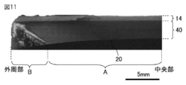
- Example 2 The seed crystal substrate 14 having a diameter of 45 mm is used, the gap between the crucible 10 and the seed crystal holding shaft 12 in the opening 28 is set to 3.0 mm, and the seed crystal substrate 14 is lifted from the liquid surface of the Si—C solution 24. A meniscus is formed at a position of 3.0 mm, the seed crystal holding shaft 12 is rotated at a speed of 100 rpm, the rotational speed of the outer peripheral portion of the lower surface of the seed crystal substrate 14 is 236 mm / sec, and the seed crystal substrate 14 is rotated in the same direction. Crystal growth was performed under the same conditions as in Example 1 except that the holding time was 360 seconds and the crystal growth time was 14 hours.
- FIG. 11 shows an optical micrograph of the cross section of the obtained grown crystal.
- the outer peripheral portion of the grown crystal had a larger growth film thickness than the central portion, and a concave crystal growth surface was obtained.
- a SiC single crystal in which no black portion was observed and no inclusion was obtained in region A.
- region B the grown crystal contained inclusions.
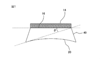
- the inclination angle ⁇ of the concave crystal growth surface with respect to the (000-1) just surface of the obtained growth crystal is 8.0 ° at the outermost peripheral portion of the region A, and the inclination angle ⁇ at the outer peripheral side is more than that. It was greater than 8.0 °.
- the crystal growth thickness at the center of the concave growth crystal surface was 2.7 mm, and the diameter of the growth surface in region A was 33.6 mm.
- Example 3 The meniscus was formed by setting the pulling position of the seed crystal substrate 14 from the liquid surface of the Si—C solution 24 to 1.7 mm, the same crystal rotation holding time of the seed crystal substrate was 7200 seconds, and the crystal growth time was 2 hours. The crystal growth was performed under the same conditions as in Example 1 except for the above.
- Example 2 In the same manner as in Example 1, a cross section of the grown crystal was cut out and mirror-polished, and observed with an optical microscope in a transmission mode.
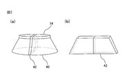
- the obtained SiC single crystal had a concave crystal growth surface 20 in which the outer peripheral portion of the grown crystal was thicker than the central portion. In the grown crystal, no black portion was observed and no inclusion was included.
- the maximum inclination angle ⁇ of the concave crystal growth surface with respect to the (000-1) just surface of the obtained growth crystal was 2.0 °.
- the crystal growth thickness at the center of the crystal growth surface was 1.2 mm, and the diameter of the growth surface of the growth crystal was 15.6 mm.
- Example 4 The meniscus is formed by setting the pulling position of the seed crystal substrate 14 from the liquid surface of the Si—C solution 24 to 1.3 mm, the rotation speed of the seed crystal holding shaft is 120 rpm, the outer peripheral speed of the seed crystal substrate is 101 mm / s, and the same Crystal growth was performed under the same conditions as in Example 1 except that the direction rotation holding time was 360 seconds and the crystal growth time was 20 hours.
- Example 2 In the same manner as in Example 1, a cross section of the grown crystal was cut out and mirror-polished, and observed with an optical microscope in a transmission mode.
- the obtained SiC single crystal had a concave crystal growth surface 20 in which the outer peripheral portion of the grown crystal was thicker than the central portion. In the grown crystal, no black portion was observed and no inclusion was included.
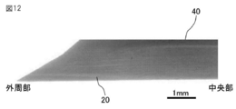
- Example 5 A seed crystal substrate having a diameter of 12 mm is used, a meniscus is formed by setting the pulling position of the seed crystal substrate 14 from the liquid surface of the Si—C solution 24 to 1.3 mm, and the rotation speed of the seed crystal holding shaft is 100 rpm.
- the crystal growth was performed under the same conditions as in Example 1 except that the outer peripheral speed was 63 mm / s, the same direction rotation holding time was 18000 seconds, and the crystal growth time was 5 hours.
- FIG. 12 shows an optical micrograph of a cross section of the obtained grown crystal.
- the obtained SiC single crystal had a concave crystal growth surface 20 in which the outer peripheral portion of the grown crystal was thicker than the central portion. In the grown crystal, no black portion was observed and no inclusion was included.
- the maximum inclination angle ⁇ of the concave crystal growth surface with respect to the (000-1) just surface of the obtained growth crystal was 2.0 °.
- the crystal growth thickness at the center of the crystal growth surface was 2.3 mm, and the diameter of the growth surface of the growth crystal was 16.0 mm.
- Example 6 Crystal growth was performed under the same conditions as in Example 5 except that the same crystal rotation holding time of the seed crystal substrate was 3600 seconds and the crystal growth time was 10 hours.
- Example 2 In the same manner as in Example 1, a cross section of the grown crystal was cut out and mirror-polished, and observed with an optical microscope in a transmission mode.
- the obtained SiC single crystal had a concave crystal growth surface 20 in which the outer peripheral portion of the grown crystal was thicker than the central portion. In the grown crystal, no black portion was observed and no inclusion was included.
- the maximum inclination angle ⁇ of the concave crystal growth surface with respect to the (000-1) just surface of the obtained growth crystal was 4.0 °.
- the crystal growth thickness at the center of the crystal growth surface was 4.5 mm, and the diameter of the growth surface of the growth crystal was 26.0 mm.
- Example 7 A meniscus was formed by setting the pulling position of the seed crystal substrate 14 from the liquid surface of the Si—C solution 24 to 1.5 mm, the same crystal rotation holding time of the seed crystal substrate was 360 seconds, and the crystal growth time was 30 hours. Except for the above, crystal growth was performed under the same conditions as in Example 5.
- Example 2 In the same manner as in Example 1, a cross section of the grown crystal was cut out and mirror-polished, and observed with an optical microscope in a transmission mode.
- the maximum inclination angle ⁇ of the concave crystal growth surface with respect to the (000-1) just surface of the obtained growth crystal was 6.0 °.
- the crystal growth thickness at the center of the crystal growth surface was 2.5 mm, and the diameter of the growth surface of the growth crystal was 19.0 mm.
- the seed crystal substrate 14 having a diameter of 25 mm was used, the gap between the crucible 10 and the seed crystal holding shaft 12 in the opening 28 was set to 1.5 mm, and the lower surface of the seed crystal substrate 14 was brought into contact with the Si—C solution 24.
- the subsequent pulling position is 1.3 mm, and during crystal growth, the seed crystal holding shaft 12 is rotated at a speed of 40 rpm, and the outermost peripheral portion of the lower surface of the seed crystal substrate 14 is rotated at a speed of 52 mm / sec. 10 is rotated in the same direction at 5 rpm, the rotation holding time for continuously rotating the seed crystal substrate in the same direction is 15 seconds, and the stop time of the seed crystal holding shaft 12 when the rotation direction is switched is 5 seconds.
- the crystal growth was performed under the same conditions as in Example 1 except that the rotation direction was changed to and the crystal growth time was 18 hours.
- the obtained SiC crystal is cut to a thickness of 1 mm so that the center portion of the growth surface is included in the horizontal direction in the growth direction, mirror-polished, and the cross section of the cut-out growth crystal is transmitted in the transmission mode.
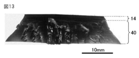
- FIG. 13 shows an optical micrograph of the obtained grown crystal.
- the obtained SiC crystal had a slightly convex growth surface with a plurality of small irregularities. Discontinuous steps were observed throughout the grown crystal, and inclusions were observed in the step part.
- the maximum inclination angle ⁇ of the crystal growth plane with respect to the (000-1) just plane of the obtained growth crystal was ⁇ 0.6 °.
- the crystal growth thickness at the center of the crystal growth surface was 8.0 mm, and the diameter of the growth surface of the growth crystal was 35.0 mm.
- the crucible 10 and the seed crystal holding shaft 12 are arranged in such a manner that the seed crystal holding shaft 12 is passed through the opening 28 opened in the upper part of the crucible 10, and a 20 mm thick heat insulating material is arranged in the opening 28.
- the clearance from the surface of the Si—C solution surface is reduced while the heat removal through the seed crystal holding shaft 12 is substantially maintained while the heat removal from the surface of the Si—C solution is reduced.
- the bottom surface of the seed crystal substrate 14 was brought into contact with the Si—C solution 24 and maintained at the same height as the liquid surface of the Si—C solution 24, and the crystal growth time was set to 5 hours. Crystal growth was performed under the following conditions.
- FIG. 15 shows an optical micrograph of the obtained grown crystal.
- the obtained SiC crystal had a convex crystal growth surface. In addition, it was confirmed that inclusions were mixed at locations where there was a growth difference in the grown crystal.
- Example 7 (Comparative Example 3) Example 7 except that a seed crystal substrate with a diameter of 16 mm was used, the gap between the crucible 10 and the seed crystal holding shaft 12 in the opening 28 was 2.0 mm, and the crystal growth time was 10 hours. Crystal growth was performed under conditions.
- FIG. 16 shows an optical micrograph of the obtained grown crystal.
- the obtained SiC crystal had a substantially flat crystal growth surface. Moreover, it was confirmed that inclusion was mixed in the grown crystal.
- the maximum inclination angle ⁇ of the crystal growth surface of the obtained grown crystal with respect to the (000-1) just surface was 0.0 °.
- the crystal growth thickness at the center of the crystal growth surface was 3.8 mm, and the diameter of the growth surface of the growth crystal was 17.1 mm.
- Example 4 A meniscus is formed by setting the pulling position of the seed crystal substrate 14 from the liquid surface of the Si—C solution 24 to 1.7 mm, the rotation speed of the seed crystal holding shaft is 40 rpm, the outer peripheral speed of the seed crystal substrate is 25 mm / s, Crystal growth was performed under the same conditions as in Example 5 except that the crucible 10 was rotated in the same direction at 5 rpm.
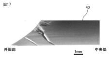
- FIG. 17 shows an optical micrograph of the obtained grown crystal.
- the obtained SiC growth crystal had a substantially flat crystal growth surface, a black portion was observed, and inclusion was included.
- the maximum inclination angle ⁇ of the crystal growth plane with respect to the (000-1) just plane of the obtained growth crystal was ⁇ 0.5 °.
- the crystal growth thickness at the center of the crystal growth surface was 2.8 mm, and the maximum diameter of the grown crystal was 16.6 mm.
- Example 2 In the same manner as in Example 1, a cross section of the grown crystal was cut out and mirror-polished, and observed with an optical microscope in a transmission mode.
- the obtained SiC growth crystal had a convex crystal growth surface, a black portion was seen, and inclusion was included.
- Example 2 In the same manner as in Example 1, a cross section of the grown crystal was cut out and mirror-polished, and observed with an optical microscope in a transmission mode.
- the obtained SiC growth crystal had a concave crystal growth surface, a black portion was seen, and inclusion was included.
- the maximum tilt angle ⁇ of the crystal growth plane with respect to the (000-1) just plane of the obtained grown crystal was ⁇ 10.0 °, and the maximum tilt angle ⁇ exceeded 8 ° in the majority of the crystal growth plane.
- the crystal growth thickness at the center of the crystal growth surface was 4.9 mm, and the maximum diameter of the grown crystal was 12.2 mm.
- Example 1 Under the conditions of Example 1 where the crystal rotation speed is as high as 126 mm / sec, the Si—C solution flows from the deep part of the Si—C solution 24 toward the central part immediately below the seed crystal substrate 14 as shown in FIG. In addition, a flow from the central portion toward the outer peripheral portion was observed, and a circulation of the Si—C solution flowing from the outer peripheral portion to the deep portion was observed, and no stagnation portion was observed immediately below the growth interface. On the other hand, in the case of the condition of Comparative Example 4 where the crystal rotation speed is as low as 25 mm / second, as shown in FIG. 20, the flow of the Si—C solution is small. In contrast to the case of Example 1, a weak flow from the outer peripheral portion toward the central portion was observed.
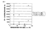
- FIG. 21 is a graph showing the relationship between the presence / absence of inclusion of the grown crystal obtained in Examples 1 and 3 to 7 and Comparative Examples 4 to 8, the peripheral speed of the seed crystal substrate, and the same direction rotation holding time.
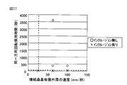
- FIG. 22 shows a graph in which the region having the short rotation holding time in the same direction in FIG.
Landscapes
- Chemical & Material Sciences (AREA)
- Engineering & Computer Science (AREA)
- Crystallography & Structural Chemistry (AREA)
- Materials Engineering (AREA)
- Metallurgy (AREA)
- Organic Chemistry (AREA)
- Inorganic Chemistry (AREA)
- Crystals, And After-Treatments Of Crystals (AREA)
Abstract
Priority Applications (4)
| Application Number | Priority Date | Filing Date | Title |
|---|---|---|---|
| KR1020157001234A KR101708131B1 (ko) | 2012-07-19 | 2013-05-08 | SiC 단결정 잉곳 및 그 제조 방법 |
| CN201380037691.6A CN104471118B (zh) | 2012-07-19 | 2013-05-08 | SiC单晶锭及其制造方法 |
| US14/415,407 US9523156B2 (en) | 2012-07-19 | 2013-05-08 | SiC single crystal ingot and production method therefor |
| EP13820560.4A EP2876190B1 (fr) | 2012-07-19 | 2013-05-08 | LINGOT DE MONOCRISTAL DE CARBURE DE SILICIUM (SiC) ET PROCÉDÉ DE PRODUCTION DE CE DERNIER |
Applications Claiming Priority (2)
| Application Number | Priority Date | Filing Date | Title |
|---|---|---|---|
| JP2012-160816 | 2012-07-19 | ||
| JP2012160816A JP6046405B2 (ja) | 2012-07-19 | 2012-07-19 | SiC単結晶のインゴット、その製造装置及びその製造方法 |
Publications (1)
| Publication Number | Publication Date |
|---|---|
| WO2014013773A1 true WO2014013773A1 (fr) | 2014-01-23 |
Family
ID=49948610
Family Applications (1)
| Application Number | Title | Priority Date | Filing Date |
|---|---|---|---|
| PCT/JP2013/062955 Ceased WO2014013773A1 (fr) | 2012-07-19 | 2013-05-08 | LINGOT DE MONOCRISTAL DE CARBURE DE SILICIUM (SiC) ET PROCÉDÉ DE PRODUCTION DE CE DERNIER |
Country Status (6)
| Country | Link |
|---|---|
| US (1) | US9523156B2 (fr) |
| EP (1) | EP2876190B1 (fr) |
| JP (1) | JP6046405B2 (fr) |
| KR (1) | KR101708131B1 (fr) |
| CN (1) | CN104471118B (fr) |
| WO (1) | WO2014013773A1 (fr) |
Cited By (5)
| Publication number | Priority date | Publication date | Assignee | Title |
|---|---|---|---|---|
| CN105401218A (zh) * | 2014-09-09 | 2016-03-16 | 丰田自动车株式会社 | SiC单晶及其制造方法 |
| CN107532329A (zh) * | 2015-03-18 | 2018-01-02 | 丰田自动车株式会社 | SiC单晶的制造方法 |
| CN107532328A (zh) * | 2015-03-18 | 2018-01-02 | 丰田自动车株式会社 | SiC单晶的制造方法 |
| US10450671B2 (en) | 2013-09-27 | 2019-10-22 | Toyota Jidosha Kabushiki Kaisha | SiC single crystal and method for producing same |
| WO2025249355A1 (fr) * | 2024-05-31 | 2025-12-04 | セントラル硝子株式会社 | TRANCHE DE MONOCRISTAL DE SiC, LINGOT DE MONOCRISTAL DE SiC, PROCÉDÉ DE PRODUCTION DE TRANCHE DE MONOCRISTAL DE SiC, PROCÉDÉ DE PRODUCTION DE LINGOT DE MONOCRISTAL DE SiC, DISPOSITIF DE PRODUCTION DE LINGOT DE MONOCRISTAL DE SiC ET PROCÉDÉ DE FORMATION DE FILM FORMÉ PAR CROISSANCE ÉPITAXIALE DE SiC |
Families Citing this family (15)
| Publication number | Priority date | Publication date | Assignee | Title |
|---|---|---|---|---|
| JP2712530B2 (ja) | 1989-04-20 | 1998-02-16 | 株式会社ニコン | トラッキング調整とマクロ撮影との切換え機構を有するレンズ鏡筒 |
| JP5925319B2 (ja) * | 2012-07-19 | 2016-05-25 | 新日鐵住金株式会社 | SiC単結晶の製造装置及びSiC単結晶の製造方法 |
| JP2015189626A (ja) * | 2014-03-28 | 2015-11-02 | 京セラ株式会社 | 結晶の製造方法 |
| JP6119732B2 (ja) * | 2014-09-09 | 2017-04-26 | トヨタ自動車株式会社 | SiC単結晶及びその製造方法 |
| JP6256411B2 (ja) * | 2015-05-18 | 2018-01-10 | トヨタ自動車株式会社 | SiC単結晶の製造方法 |
| CN107683520B (zh) | 2015-10-26 | 2021-01-26 | 株式会社Lg化学 | 基于硅的熔融组合物和使用其的SiC单晶的制造方法 |
| JP6390628B2 (ja) * | 2016-01-12 | 2018-09-19 | トヨタ自動車株式会社 | SiC単結晶の製造方法及び製造装置 |
| JP6500828B2 (ja) * | 2016-04-26 | 2019-04-17 | トヨタ自動車株式会社 | SiC単結晶の製造方法 |
| US20170327968A1 (en) * | 2016-05-10 | 2017-11-16 | Toyota Jidosha Kabushiki Kaisha | SiC SINGLE CRYSTAL AND METHOD FOR PRODUCING SAME |
| CN106012021B (zh) * | 2016-06-30 | 2019-04-12 | 山东天岳先进材料科技有限公司 | 一种液相生长碳化硅的籽晶轴及方法 |
| JP6558394B2 (ja) | 2017-04-26 | 2019-08-14 | トヨタ自動車株式会社 | SiC単結晶の製造方法及び製造装置 |
| JP7170521B2 (ja) * | 2018-12-05 | 2022-11-14 | 昭和電工株式会社 | SiC単結晶の評価用サンプル取得方法 |
| TWI777692B (zh) * | 2020-08-17 | 2022-09-11 | 環球晶圓股份有限公司 | 碳化矽晶圓及其製備方法 |
| JP2022085346A (ja) * | 2020-11-27 | 2022-06-08 | 昭和電工株式会社 | SiC単結晶の製造方法 |
| CN116500290B (zh) * | 2023-06-21 | 2023-09-08 | 长沙海纳光电科技有限公司 | 一种基于透射法的过饱和固体药剂添加装置和方法 |
Citations (5)
| Publication number | Priority date | Publication date | Assignee | Title |
|---|---|---|---|---|
| JP2006117441A (ja) | 2004-10-19 | 2006-05-11 | Sumitomo Metal Ind Ltd | 炭化珪素単結晶の製造方法 |
| JP2007186374A (ja) * | 2006-01-12 | 2007-07-26 | Toyota Motor Corp | SiC単結晶の製造方法 |
| JP2010184838A (ja) * | 2009-02-12 | 2010-08-26 | Toyota Motor Corp | 溶液法によるSiC単結晶製造装置 |
| JP2010208926A (ja) * | 2009-03-12 | 2010-09-24 | Toyota Motor Corp | SiC単結晶の製造方法 |
| JP2010248003A (ja) * | 2009-04-10 | 2010-11-04 | Toyota Motor Corp | SiC単結晶の製造方法 |
Family Cites Families (11)
| Publication number | Priority date | Publication date | Assignee | Title |
|---|---|---|---|---|
| JP2005089223A (ja) * | 2003-09-16 | 2005-04-07 | Tdk Corp | 単結晶及びその製造方法 |
| WO2006025420A1 (fr) | 2004-09-03 | 2006-03-09 | Sumitomo Metal Industries, Ltd. | Procédé pour la préparation d’un monocristal de carbure de silicium |
| JP4844127B2 (ja) * | 2006-01-11 | 2011-12-28 | 株式会社Sumco | 単結晶製造装置および製造方法 |
| JP4853449B2 (ja) * | 2007-10-11 | 2012-01-11 | 住友金属工業株式会社 | SiC単結晶の製造方法、SiC単結晶ウエハ及びSiC半導体デバイス |
| KR101310546B1 (ko) * | 2008-08-29 | 2013-09-23 | 신닛테츠스미킨 카부시키카이샤 | 탄화규소 단결정의 제조 방법 |
| KR101454978B1 (ko) | 2009-08-27 | 2014-10-27 | 신닛테츠스미킨 카부시키카이샤 | SiC 단결정 웨이퍼와 그 제조 방법 |
| JP5434801B2 (ja) | 2010-06-03 | 2014-03-05 | トヨタ自動車株式会社 | SiC単結晶の製造方法 |
| JP5656623B2 (ja) | 2010-12-28 | 2015-01-21 | トヨタ自動車株式会社 | SiC単結晶の製造装置および製造方法 |
| WO2012127703A1 (fr) | 2011-03-23 | 2012-09-27 | トヨタ自動車株式会社 | Procédé permettant de produire des monocristaux de sic et dispositif de production |
| US9777396B2 (en) | 2011-10-28 | 2017-10-03 | Kyocera Corporation | Method for producing crystal |
| JP5801730B2 (ja) | 2012-01-20 | 2015-10-28 | トヨタ自動車株式会社 | 単結晶の製造装置に用いられる種結晶保持軸及び単結晶の製造方法 |
-
2012
- 2012-07-19 JP JP2012160816A patent/JP6046405B2/ja active Active
-
2013
- 2013-05-08 US US14/415,407 patent/US9523156B2/en active Active
- 2013-05-08 WO PCT/JP2013/062955 patent/WO2014013773A1/fr not_active Ceased
- 2013-05-08 CN CN201380037691.6A patent/CN104471118B/zh active Active
- 2013-05-08 KR KR1020157001234A patent/KR101708131B1/ko not_active Expired - Fee Related
- 2013-05-08 EP EP13820560.4A patent/EP2876190B1/fr active Active
Patent Citations (5)
| Publication number | Priority date | Publication date | Assignee | Title |
|---|---|---|---|---|
| JP2006117441A (ja) | 2004-10-19 | 2006-05-11 | Sumitomo Metal Ind Ltd | 炭化珪素単結晶の製造方法 |
| JP2007186374A (ja) * | 2006-01-12 | 2007-07-26 | Toyota Motor Corp | SiC単結晶の製造方法 |
| JP2010184838A (ja) * | 2009-02-12 | 2010-08-26 | Toyota Motor Corp | 溶液法によるSiC単結晶製造装置 |
| JP2010208926A (ja) * | 2009-03-12 | 2010-09-24 | Toyota Motor Corp | SiC単結晶の製造方法 |
| JP2010248003A (ja) * | 2009-04-10 | 2010-11-04 | Toyota Motor Corp | SiC単結晶の製造方法 |
Cited By (9)
| Publication number | Priority date | Publication date | Assignee | Title |
|---|---|---|---|---|
| US10450671B2 (en) | 2013-09-27 | 2019-10-22 | Toyota Jidosha Kabushiki Kaisha | SiC single crystal and method for producing same |
| EP3051009B1 (fr) * | 2013-09-27 | 2020-12-16 | Toyota Jidosha Kabushiki Kaisha | Monocristal de sic et procédé de production de celui-ci |
| CN105401218A (zh) * | 2014-09-09 | 2016-03-16 | 丰田自动车株式会社 | SiC单晶及其制造方法 |
| US9732437B2 (en) | 2014-09-09 | 2017-08-15 | Toyota Jidosha Kabushiki Kaisha | SiC single crystal and method for producing same |
| CN107532329A (zh) * | 2015-03-18 | 2018-01-02 | 丰田自动车株式会社 | SiC单晶的制造方法 |
| CN107532328A (zh) * | 2015-03-18 | 2018-01-02 | 丰田自动车株式会社 | SiC单晶的制造方法 |
| CN107532328B (zh) * | 2015-03-18 | 2020-06-19 | 丰田自动车株式会社 | SiC单晶的制造方法 |
| CN107532329B (zh) * | 2015-03-18 | 2020-06-26 | 丰田自动车株式会社 | SiC单晶的制造方法 |
| WO2025249355A1 (fr) * | 2024-05-31 | 2025-12-04 | セントラル硝子株式会社 | TRANCHE DE MONOCRISTAL DE SiC, LINGOT DE MONOCRISTAL DE SiC, PROCÉDÉ DE PRODUCTION DE TRANCHE DE MONOCRISTAL DE SiC, PROCÉDÉ DE PRODUCTION DE LINGOT DE MONOCRISTAL DE SiC, DISPOSITIF DE PRODUCTION DE LINGOT DE MONOCRISTAL DE SiC ET PROCÉDÉ DE FORMATION DE FILM FORMÉ PAR CROISSANCE ÉPITAXIALE DE SiC |
Also Published As
| Publication number | Publication date |
|---|---|
| JP6046405B2 (ja) | 2016-12-14 |
| KR101708131B1 (ko) | 2017-02-17 |
| EP2876190A4 (fr) | 2015-11-04 |
| KR20150023031A (ko) | 2015-03-04 |
| EP2876190A1 (fr) | 2015-05-27 |
| CN104471118B (zh) | 2017-10-27 |
| CN104471118A (zh) | 2015-03-25 |
| EP2876190B1 (fr) | 2020-08-19 |
| US9523156B2 (en) | 2016-12-20 |
| US20150167196A1 (en) | 2015-06-18 |
| JP2014019614A (ja) | 2014-02-03 |
Similar Documents
| Publication | Publication Date | Title |
|---|---|---|
| JP6046405B2 (ja) | SiC単結晶のインゴット、その製造装置及びその製造方法 | |
| JP5821958B2 (ja) | SiC単結晶及びその製造方法 | |
| JP5839117B2 (ja) | SiC単結晶及びその製造方法 | |
| JP5905864B2 (ja) | SiC単結晶及びその製造方法 | |
| JP5876390B2 (ja) | SiC単結晶の製造方法 | |
| JP2016064958A (ja) | SiC単結晶の製造方法 | |
| JP6354615B2 (ja) | SiC単結晶の製造方法 | |
| JP2017202969A (ja) | SiC単結晶及びその製造方法 | |
| JP6390628B2 (ja) | SiC単結晶の製造方法及び製造装置 | |
| JP6060863B2 (ja) | SiC単結晶及びその製造方法 | |
| JP2017226583A (ja) | SiC単結晶の製造方法 | |
| JPWO2018062224A1 (ja) | SiC単結晶の製造方法及びSiC種結晶 | |
| JP6030525B2 (ja) | SiC単結晶の製造方法 | |
| JP6500828B2 (ja) | SiC単結晶の製造方法 |
Legal Events
| Date | Code | Title | Description |
|---|---|---|---|
| 121 | Ep: the epo has been informed by wipo that ep was designated in this application |
Ref document number: 13820560 Country of ref document: EP Kind code of ref document: A1 |
|
| ENP | Entry into the national phase |
Ref document number: 20157001234 Country of ref document: KR Kind code of ref document: A |
|
| WWE | Wipo information: entry into national phase |
Ref document number: 14415407 Country of ref document: US |
|
| NENP | Non-entry into the national phase |
Ref country code: DE |
|
| WWE | Wipo information: entry into national phase |
Ref document number: 2013820560 Country of ref document: EP |