WO2014034396A1 - プラズマ処理方法、及びプラズマ処理装置 - Google Patents
プラズマ処理方法、及びプラズマ処理装置 Download PDFInfo
- Publication number
- WO2014034396A1 WO2014034396A1 PCT/JP2013/071409 JP2013071409W WO2014034396A1 WO 2014034396 A1 WO2014034396 A1 WO 2014034396A1 JP 2013071409 W JP2013071409 W JP 2013071409W WO 2014034396 A1 WO2014034396 A1 WO 2014034396A1
- Authority
- WO
- WIPO (PCT)
- Prior art keywords
- gas
- plasma processing
- plasma
- fluorine
- titanium
- Prior art date
- Legal status (The legal status is an assumption and is not a legal conclusion. Google has not performed a legal analysis and makes no representation as to the accuracy of the status listed.)
- Ceased
Links
Images






Classifications
-
- H—ELECTRICITY
- H01—ELECTRIC ELEMENTS
- H01J—ELECTRIC DISCHARGE TUBES OR DISCHARGE LAMPS
- H01J37/00—Discharge tubes with provision for introducing objects or material to be exposed to the discharge, e.g. for the purpose of examination or processing thereof
- H01J37/32—Gas-filled discharge tubes
- H01J37/32431—Constructional details of the reactor
- H01J37/3244—Gas supply means
-
- H—ELECTRICITY
- H01—ELECTRIC ELEMENTS
- H01J—ELECTRIC DISCHARGE TUBES OR DISCHARGE LAMPS
- H01J37/00—Discharge tubes with provision for introducing objects or material to be exposed to the discharge, e.g. for the purpose of examination or processing thereof
- H01J37/32—Gas-filled discharge tubes
- H01J37/32009—Arrangements for generation of plasma specially adapted for examination or treatment of objects, e.g. plasma sources
- H01J37/32082—Radio frequency generated discharge
- H01J37/32091—Radio frequency generated discharge the radio frequency energy being capacitively coupled to the plasma
-
- C—CHEMISTRY; METALLURGY
- C23—COATING METALLIC MATERIAL; COATING MATERIAL WITH METALLIC MATERIAL; CHEMICAL SURFACE TREATMENT; DIFFUSION TREATMENT OF METALLIC MATERIAL; COATING BY VACUUM EVAPORATION, BY SPUTTERING, BY ION IMPLANTATION OR BY CHEMICAL VAPOUR DEPOSITION, IN GENERAL; INHIBITING CORROSION OF METALLIC MATERIAL OR INCRUSTATION IN GENERAL
- C23F—NON-MECHANICAL REMOVAL OF METALLIC MATERIAL FROM SURFACE; INHIBITING CORROSION OF METALLIC MATERIAL OR INCRUSTATION IN GENERAL; MULTI-STEP PROCESSES FOR SURFACE TREATMENT OF METALLIC MATERIAL INVOLVING AT LEAST ONE PROCESS PROVIDED FOR IN CLASS C23 AND AT LEAST ONE PROCESS COVERED BY SUBCLASS C21D OR C22F OR CLASS C25
- C23F4/00—Processes for removing metallic material from surfaces, not provided for in group C23F1/00 or C23F3/00
-
- H—ELECTRICITY
- H01—ELECTRIC ELEMENTS
- H01J—ELECTRIC DISCHARGE TUBES OR DISCHARGE LAMPS
- H01J37/00—Discharge tubes with provision for introducing objects or material to be exposed to the discharge, e.g. for the purpose of examination or processing thereof
- H01J37/32—Gas-filled discharge tubes
- H01J37/32009—Arrangements for generation of plasma specially adapted for examination or treatment of objects, e.g. plasma sources
- H01J37/32082—Radio frequency generated discharge
- H01J37/32137—Radio frequency generated discharge controlling of the discharge by modulation of energy
- H01J37/32155—Frequency modulation
- H01J37/32165—Plural frequencies
-
- H—ELECTRICITY
- H01—ELECTRIC ELEMENTS
- H01J—ELECTRIC DISCHARGE TUBES OR DISCHARGE LAMPS
- H01J37/00—Discharge tubes with provision for introducing objects or material to be exposed to the discharge, e.g. for the purpose of examination or processing thereof
- H01J37/32—Gas-filled discharge tubes
- H01J37/32431—Constructional details of the reactor
- H01J37/3244—Gas supply means
- H01J37/32449—Gas control, e.g. control of the gas flow
-
- H—ELECTRICITY
- H01—ELECTRIC ELEMENTS
- H01J—ELECTRIC DISCHARGE TUBES OR DISCHARGE LAMPS
- H01J37/00—Discharge tubes with provision for introducing objects or material to be exposed to the discharge, e.g. for the purpose of examination or processing thereof
- H01J37/32—Gas-filled discharge tubes
- H01J37/32431—Constructional details of the reactor
- H01J37/32458—Vessel
-
- H—ELECTRICITY
- H01—ELECTRIC ELEMENTS
- H01J—ELECTRIC DISCHARGE TUBES OR DISCHARGE LAMPS
- H01J37/00—Discharge tubes with provision for introducing objects or material to be exposed to the discharge, e.g. for the purpose of examination or processing thereof
- H01J37/32—Gas-filled discharge tubes
- H01J37/32431—Constructional details of the reactor
- H01J37/32798—Further details of plasma apparatus not provided for in groups H01J37/3244 - H01J37/32788; special provisions for cleaning or maintenance of the apparatus
- H01J37/32853—Hygiene
- H01J37/32862—In situ cleaning of vessels and/or internal parts
-
- H—ELECTRICITY
- H10—SEMICONDUCTOR DEVICES; ELECTRIC SOLID-STATE DEVICES NOT OTHERWISE PROVIDED FOR
- H10P—GENERIC PROCESSES OR APPARATUS FOR THE MANUFACTURE OR TREATMENT OF DEVICES COVERED BY CLASS H10
- H10P50/00—Etching of wafers, substrates or parts of devices
- H10P50/20—Dry etching; Plasma etching; Reactive-ion etching
- H10P50/28—Dry etching; Plasma etching; Reactive-ion etching of insulating materials
- H10P50/282—Dry etching; Plasma etching; Reactive-ion etching of insulating materials of inorganic materials
- H10P50/283—Dry etching; Plasma etching; Reactive-ion etching of insulating materials of inorganic materials by chemical means
-
- H—ELECTRICITY
- H10—SEMICONDUCTOR DEVICES; ELECTRIC SOLID-STATE DEVICES NOT OTHERWISE PROVIDED FOR
- H10P—GENERIC PROCESSES OR APPARATUS FOR THE MANUFACTURE OR TREATMENT OF DEVICES COVERED BY CLASS H10
- H10P50/00—Etching of wafers, substrates or parts of devices
- H10P50/73—Etching of wafers, substrates or parts of devices using masks for insulating materials
-
- H—ELECTRICITY
- H01—ELECTRIC ELEMENTS
- H01J—ELECTRIC DISCHARGE TUBES OR DISCHARGE LAMPS
- H01J2237/00—Discharge tubes exposing object to beam, e.g. for analysis treatment, etching, imaging
- H01J2237/32—Processing objects by plasma generation
- H01J2237/33—Processing objects by plasma generation characterised by the type of processing
- H01J2237/334—Etching
Definitions
- Various aspects and embodiments of the present invention relate to a plasma processing method and a plasma processing apparatus.
- plasma processing apparatuses that perform plasma processing for the purpose of thin film deposition or etching are widely used.
- the plasma processing apparatus include a plasma CVD (Chemical Vapor Deposition) apparatus that performs a thin film deposition process, a plasma etching apparatus that performs an etching process, and the like.
- the plasma processing apparatus includes, for example, a processing container that defines a plasma processing space, a sample stage in which a substrate to be processed is installed in the processing container, and a gas supply system for introducing a processing gas necessary for the plasma reaction into the processing chamber.
- the plasma processing apparatus is installed on the sample stage by applying a plasma generation mechanism that supplies electromagnetic energy such as microwaves and RF waves to the sample stage and a bias voltage in order to turn the processing gas in the processing chamber into plasma.
- a bias voltage application mechanism for accelerating ions in the plasma toward the substrate to be processed.
- a mask film of a titanium-containing material for example, TiN
- a mask film of a titanium-containing material for example, TiN
- the mask film is disposed in the processing container so as to face the plasma processing space. It is disclosed that a substrate to be processed is etched using a mask film as a mask.
- the conventional technique has a problem that the etching characteristics of the substrate to be processed may deteriorate over time. That is, in the prior art, when the substrate to be processed is etched using the TiN mask film as a mask, the mask film itself is etched simultaneously with the etching of the insulating film in the opening of the etching pattern. For this reason, in the prior art, deposits such as titanium-containing materials generated from the etched mask film are accumulated on various members facing the plasma processing space, and the plasma density in the plasma processing space fluctuates. As a result, the etching characteristics of the substrate to be processed may deteriorate over time. In particular, when a plurality of substrates to be processed are processed, this deterioration with time becomes significant.
- a plasma processing method is a plasma processing method in a plasma processing apparatus.
- the plasma processing method includes a first step, a second step, and a third step.
- the first fluorine-containing gas is supplied to the plasma processing space, and the substrate to be processed on which the mask film of the titanium-containing material is formed on the surface of the insulating film uses the plasma of the first fluorine-containing gas.
- etch In the second step, O 2 gas is supplied to the plasma processing space, and the carbon-containing material attached after the first step to the member disposed with the surface facing the plasma processing space is added to the O 2 gas. Removal is performed using two gas plasma.
- a nitrogen-containing gas and a second fluorine-containing gas are supplied to the plasma processing space, and the titanium-containing material attached to the member after the first step is removed from the nitrogen-containing gas and the first gas. 2 using a fluorine-containing gas plasma.
- a plasma processing method and a plasma processing apparatus capable of suppressing deterioration with time of etching characteristics of a substrate to be processed are realized.
- FIG. 1 is a longitudinal sectional view showing an outline of a configuration of a plasma processing apparatus according to an embodiment.
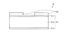
- FIG. 2A is a diagram illustrating a configuration example of a wafer before being etched using the plasma processing apparatus according to the embodiment.
- FIG. 2B is a diagram illustrating a configuration example of a wafer after being etched using the plasma processing apparatus according to an embodiment.
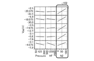
- FIG. 3A is a diagram showing a result of executing an experimental design method for selecting elements that contribute to the removal of titanium-containing materials.
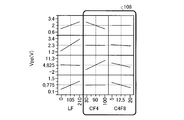
- FIG. 3B is a diagram illustrating a result of executing an experimental design method for selecting elements that contribute to the removal of titanium-containing materials.
- FIG. 1 is a longitudinal sectional view showing an outline of a configuration of a plasma processing apparatus according to an embodiment.
- FIG. 2A is a diagram illustrating a configuration example of a wafer before being etched using the plasma processing apparatus according to the embodiment.
- FIG. 2B is a diagram illustrating a configuration example of a wa
- FIG. 3C is a diagram illustrating a result of executing an experimental design method for selecting elements that contribute to the removal of titanium-containing materials.
- FIG. 3D is a diagram illustrating a result of executing an experimental design method for selecting elements that contribute to the removal of the titanium-containing material.
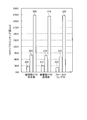
- FIG. 4 is a diagram showing the etching amount of the titanium-containing material for each member arranged with the surface facing the plasma processing space.
- FIG. 5A is a diagram illustrating a plasma processing model of the present embodiment.
- FIG. 5B is a diagram illustrating a plasma processing model of the present embodiment.
- FIG. 5C is a diagram illustrating a plasma processing model of the present embodiment.
- FIG. 6 is a flowchart of the plasma processing of the first embodiment.
- FIG. 5A is a diagram illustrating a plasma processing model of the present embodiment.
- FIG. 5B is a diagram illustrating a plasma processing model of the present embodiment.
- FIG. 5C is a diagram illustrating a plasma processing model of
- FIG. 7 is a diagram showing a flowchart of the plasma processing of the second embodiment.
- FIG. 8 is a flowchart of the plasma processing according to the third embodiment.
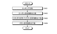
- FIG. 9 is a view showing a flowchart of the plasma processing of the fourth embodiment.
- FIG. 10A is a diagram (No. 1) for describing an effect of the plasma processing method of the present embodiment.
- FIG. 10B is a diagram (No. 1) for describing an effect of the plasma processing method of the present embodiment.
- FIG. 11 is a diagram (No. 2) for explaining the effect of the plasma processing method of the present embodiment.
- the first fluorine-containing gas is supplied to the plasma processing space, and the substrate to be processed having the titanium-containing material mask film formed on the surface of the insulating film is etched using the first fluorine-containing gas plasma.
- a first step of supplying the O 2 gas to the plasma processing space, and the carbon-containing material adhering after the first step to the member disposed with the surface facing the plasma processing space of the O 2 gas A second step of removing using plasma, a nitrogen-containing gas and a second fluorine-containing gas are supplied to the plasma processing space, and the titanium-containing material adhering to the member after the first step is removed from the nitrogen-containing gas and And a third step of removing using plasma of the second fluorine-containing gas.
- the plasma processing method supplies a third fluorine-containing gas to the plasma processing space between the second step and the third step, and adheres to the member after the first step.
- a fourth step of removing the titanium-containing material by using a plasma of a third fluorine-containing gas is further included.
- the plasma processing method is such that the plasma processing apparatus repeats the second step and the third step at least twice after executing the first step.
- the nitrogen-containing gas is N 2 gas or NF 3 gas
- the second fluorine-containing gas is CF 4 gas, C 4 F 8 gas, or CHF 3 gas.
- a plasma processing apparatus includes a processing container that defines a plasma processing space in which a substrate to be processed in which a mask film of a titanium-containing material is formed on the surface of an insulating film, and a first fluorine-containing gas.
- a first gas supply unit that supplies gas to the plasma processing space, a second gas supply unit that supplies O 2 gas to the plasma processing space, and a nitrogen-containing gas and a second fluorine-containing gas to the plasma processing space A first step of supplying a first fluorine-containing gas from the third gas supply unit and the first gas supply unit to the plasma processing space and etching the substrate to be processed using the plasma of the first fluorine-containing gas; Then, O 2 gas is supplied from the second gas supply unit to the plasma processing space, and the carbon-containing material attached after the first step to the member disposed with the surface facing the plasma processing space is O 2.
- the second step of removing using the plasma of the second step, the nitrogen-containing gas and the second fluorine-containing gas from the third gas supply unit are supplied to the plasma processing space, and adhere to the member after the first step
- a control unit that executes a third step of removing the titanium-containing material using the plasma of the nitrogen-containing gas and the second fluorine-containing gas.
- FIG. 1 is a longitudinal sectional view showing an outline of a configuration of a plasma processing apparatus according to an embodiment.
- the plasma processing apparatus 1 has a substantially cylindrical processing container 11 that defines a plasma processing space S for performing plasma processing.
- the processing container 11 is electrically connected to the ground line 12 and grounded. Further, the surface of the processing container 11 faces the plasma processing space S. That is, the processing vessel 11 is provided with the surface facing the plasma processing space S.
- a wafer chuck 10 that holds a wafer W as a substrate to be processed is provided.
- the wafer W held by the wafer chuck 10 is arranged with a mask film D2 of the wafer W described later facing the plasma processing space S.
- the lower surface of the wafer chuck 10 is supported by a susceptor 13 serving as a lower electrode.
- the susceptor 13 is formed in a substantially disk shape from a metal such as aluminum.
- a support base 15 is provided at the bottom of the processing container 11 via an insulating plate 14, and the susceptor 13 is supported on the upper surface of the support base 15.
- An electrode (not shown) is provided inside the wafer chuck 10 so that the wafer W can be attracted and held by an electrostatic force generated by applying a DC voltage to the electrode.
- a conductive focus ring 20 made of, for example, silicon is provided on the outer surface of the wafer chuck 10 on the upper surface of the susceptor 13 to improve the uniformity of plasma processing.
- the outer surface of the susceptor 13, the support base 15, and the focus ring 20 is covered with a cylindrical member 21 made of, for example, quartz. Further, the surface of the focus ring 20 faces the plasma processing space S. That is, the focus ring 20 is provided with the surface facing the plasma processing space S.
- a coolant path 15a through which a coolant flows is provided in the support base 15 in, for example, an annular shape.
- the wafer W held by the wafer chuck 10 is controlled.
- the temperature can be controlled.
- the susceptor 13 is electrically connected via a first matching unit 31 to a first high-frequency power source 30 for supplying high-frequency power to the susceptor 13 to generate plasma.
- the first high frequency power supply 30 is configured to output a high frequency power of, for example, 27 to 100 MHz, for example, 40 MHz in the present embodiment.
- the first matching unit 31 matches the internal impedance of the first high-frequency power source 30 and the load impedance, and when the plasma is generated in the processing container 11, the internal impedance of the first high-frequency power source 30. And the load impedance seem to coincide with each other.
- the susceptor 13 is provided with a second high-frequency power supply 40 for supplying ions to the wafer W by supplying a high-frequency power to the susceptor 13 and applying a bias to the wafer W via a second matching unit 41.
- the second high frequency power supply 40 generates a high frequency power of, for example, 400 kHz to 13.56 MHz, which is lower than the frequency of the high frequency power output from the first high frequency power supply 30, for example, 13.56 MHz in this embodiment. It is configured to output. Similar to the first matching unit 31, the second matching unit 41 matches the internal impedance of the second high-frequency power source 40 with the load impedance.
- the high-frequency power output from the first high-frequency power supply 30 and the high-frequency power output from the second high-frequency power supply 40 may be referred to as “high-frequency power HF” and “high-frequency power LF”, respectively.
- high-frequency power HF high-frequency power HF
- high-frequency power LF high-frequency power LF
- the first high-frequency power source 30, the first matching unit 31, the second high-frequency power source 40, and the second matching unit 41 are connected to a control unit 150 described later, and these operations are controlled by the control unit 150. Is done.
- an upper electrode 42 is provided in parallel to face the susceptor 13.
- the upper electrode 42 is supported on the upper portion of the processing container 11 via a conductive support member 50. Therefore, the upper electrode 42 is at the ground potential as in the processing container 11.
- the upper electrode 42 includes an electrode plate 51 that forms an opposing surface to the wafer W held by the wafer chuck 10, and an electrode support 52 that supports the electrode plate 51 from above.
- a plurality of gas supply ports 53 for supplying a processing gas into the processing container 11 are formed so as to penetrate the electrode plate 51.
- the electrode plate 51 is made of, for example, a low-resistance conductor or semiconductor with low Joule heat, and silicon, for example, is used in the present embodiment.
- the surface of the electrode plate 51 that faces the wafer W faces the plasma processing space S. That is, the electrode plate 51 is provided with the surface facing the plasma processing space S.
- the electrode support 52 is made of a conductor, and for example, aluminum is used in the present embodiment.
- a gas diffusion chamber 54 formed in a substantially disk shape is provided in the center portion inside the electrode support 52.
- a plurality of gas holes 55 extending downward from the gas diffusion chamber 54 are formed in the lower part of the electrode support 52, and the gas supply port 53 is connected to the gas diffusion chamber 54 through the gas hole 55.
- a gas supply pipe 71 is connected to the gas diffusion chamber 54.
- a processing gas supply source 72 is connected to the gas supply pipe 71 as shown in FIG. 1, and the processing gas supplied from the processing gas supply source 72 is supplied to the gas diffusion chamber 54 via the gas supply pipe 71. Is done.
- the processing gas supplied to the gas diffusion chamber 54 is introduced into the processing container 11 through the gas hole 55 and the gas supply port 53. That is, the upper electrode 42 functions as a shower head that supplies a processing gas into the processing container 11.
- the processing gas supply source 72 in the present embodiment includes a gas supply unit 72a, a gas supply unit 72b, a gas supply unit 72c, and a gas supply unit 72d.
- the gas supply unit 72a supplies the first fluorine-containing gas to the plasma processing space S as an etching process gas.
- the first fluorine-containing gas is, for example, C 4 F 8 gas.
- the gas supply unit 72a is an example of a first gas supply unit that supplies the first fluorine-containing gas to the plasma processing space S.
- the gas supply unit 72b supplies O 2 gas to the plasma processing space S as a gas for deposit removal processing after the etching processing.
- the gas supply unit 72b is an example of a second gas supply unit that supplies O 2 gas to the plasma processing space S.
- the gas supply unit 72c supplies a nitrogen-containing gas to the plasma processing space S as a gas for deposit removal processing after the etching processing.
- the nitrogen-containing gas is, for example, N 2 gas or NF 3 gas.
- the gas supply unit 72d supplies the second fluorine-containing gas to the plasma processing space S as a gas for deposit removal processing after the etching processing.
- the second fluorine-containing gas is, for example, CF 4 gas, C 4 F 8 gas, or CHF 3 gas.
- the gas supply unit 72c and the gas supply unit 72d are an example of a third gas supply unit that supplies the nitrogen-containing gas and the second fluorine-containing gas to the plasma processing space S.
- the gas supply unit 72d can also supply the third fluorine-containing gas to the plasma processing space S as a gas for deposit removal processing after the etching processing.
- the third fluorine-containing gas is, for example, CHF 3 gas.
- the processing gas supply source 72 includes valves 73a, 73b, 73c, 73d provided between the gas supply units 72a, 72b, 72c, 72d and the gas diffusion chamber 54, and flow rate adjusting mechanisms 74a, 74b, 74c, 74d.
- the flow rate of the gas supplied to the gas diffusion chamber 54 is controlled by the flow rate adjusting mechanisms 74a, 74b, 74c, and 74d.
- An exhaust flow path 80 that functions as a flow path for discharging the atmosphere in the processing container 11 to the outside of the processing container 11 by the inner wall of the processing container 11 and the outer surface of the cylindrical member 21 at the bottom of the processing container 11. Is formed.
- An exhaust port 90 is provided on the bottom surface of the processing container 11.
- An exhaust chamber 91 is formed below the exhaust port 90, and an exhaust device 93 is connected to the exhaust chamber 91 via an exhaust pipe 92. Therefore, by driving the exhaust device 93, the atmosphere in the processing container 11 can be exhausted through the exhaust passage 80 and the exhaust port 90, and the inside of the processing container can be decompressed to a predetermined degree of vacuum.
- the plasma processing apparatus 1 is provided with a control unit 150.
- the control unit 150 is a computer, for example, and has a program storage unit (not shown) that is a storage device such as a memory.
- the program storage unit also stores a program for operating the plasma processing apparatus 1 by controlling the power supplies 30 and 40, the matching units 31 and 41, the flow rate adjusting mechanism 74, and the like.
- the control unit 150 performs control to supply the first fluorine-containing gas from the gas supply unit 72a to the plasma processing space S and to etch the wafer W using the plasma of the first fluorine-containing gas.
- control unit 150 supplies O 2 gas from the gas supply unit 72b to the plasma processing space S, and members (for example, the processing container 11, the electrode plate 51, and the like) disposed with the surface facing the plasma processing space S.
- the focus ring 20 or the like) is controlled to remove the carbon-containing material adhering after the etching of the wafer W by using O 2 gas plasma.
- control unit 150 supplies the nitrogen-containing gas and the second fluorine-containing gas from the gas supply unit 72c and the gas supply unit 72d to the plasma processing space S, and the surface is opposed to the plasma processing space S. Control is performed to remove the titanium-containing material adhering to the formed member after etching of the wafer W using the plasma of the nitrogen-containing gas and the second fluorine-containing gas.
- the above program is recorded on a computer-readable storage medium such as a computer-readable hard disk (HD), flexible disk (FD), compact disk (CD), magnetic optical desk (MO), or memory card. May have been installed in the control unit 150 from the storage medium.
- a computer-readable storage medium such as a computer-readable hard disk (HD), flexible disk (FD), compact disk (CD), magnetic optical desk (MO), or memory card. May have been installed in the control unit 150 from the storage medium.
- FIG. 2A is a diagram illustrating a configuration example of a wafer before being etched using the plasma processing apparatus according to the embodiment.
- FIG. 2B is a diagram illustrating a configuration example of a wafer after being etched using the plasma processing apparatus according to an embodiment.
- the wafer W has an insulating film D1 and a mask film D2 formed on the surface of the insulating film D1.
- the insulating film D1 is an interlayer insulating film for dual damascene wiring, and includes a first insulating film D11, a second insulating film D12, and a third insulating film D13.
- the first insulating film D11 is made of, for example, SiON.
- the second insulating film D12 is formed of a low dielectric constant material whose relative dielectric constant is a predetermined value (for example, 4.2) or less.
- the second insulating film D12 is made of, for example, SiOCH.
- the third insulating film D13 is formed of, for example, SiCN.
- the mask film D2 on which the etching pattern having a predetermined opening is formed is formed of a titanium-containing material having plasma resistance.
- the mask film D2 is made of, for example, TiN.
- the wafer W on which the titanium-containing mask film D2 is formed on the surface of the insulating film D1 is disposed with the mask film D2 facing the plasma processing space S.
- the wafer W on which the mask film D2 made of a titanium-containing material (for example, TiN) is formed on the surface of the insulating film D1 is disposed with the mask film D2 facing the plasma processing space S.
- the wafer W is etched using a TiN mask film D 2 (hereinafter referred to as “TiN film” as appropriate) as a mask
- TiN film As appropriate
- the opening of the etching pattern opening of the mask film D 2
- the insulating film D1 (the first insulating film D11 and the second insulating film D12) is etched.
- the TiN film itself is etched as indicated by a broken line in FIG. 2B.
- the titanium-containing material generated from the TiN film is disposed on the plasma processing space S with the surface facing the member (for example, the processing container 11). , The electrode plate 51 and the focus ring 20). If the titanium-containing material is cumulatively attached to the member disposed with the surface facing the plasma processing space S, the plasma density in the plasma processing space S fluctuates, and as a result, the etching characteristics of the wafer W may deteriorate over time. There is.
- the present inventors have earnestly studied on a method for efficiently removing the titanium-containing material attached after the etching of the wafer W to the member disposed with the surface facing the plasma processing space S. Piled up. As a result, the present inventors removed the carbon-containing material using O 2 gas plasma, and removed the titanium-containing material using nitrogen-containing gas and fluorine-containing gas plasma, thereby removing the titanium-containing material. The knowledge that it can remove efficiently was acquired. Hereinafter, this knowledge will be described.
- the electrode plate 51 of the upper electrode 42 is described as an example of a member disposed with the surface facing the plasma processing space S, but the present invention is not limited to this.
- the present embodiment can be similarly applied to other members such as the processing container 11 and the focus ring 20 as long as the members are disposed with the surface facing the plasma processing space S.
- 3A to 3D are diagrams showing the results of executing the experimental design method for selecting elements that contribute to the removal of titanium-containing materials.
- a result of executing an experimental design method in which a wafer W on which a TiN film as an example of a titanium-containing material adhering to the upper electrode 42 is formed is etched while changing a plurality of parameters is shown.
- the horizontal axis indicates the value of each parameter that contributes to the removal of the titanium-containing material when the experimental design method is executed.
- the vertical axis indicates Vpp (V) of the wafer W when the high frequency power HF is output from the first high frequency power supply 30.
- the vertical axis indicates Vpp (V) of the wafer W when the high frequency power LF is output from the second high frequency power supply 40.
- Vpp is a difference between the maximum value and the minimum value of the voltage value of the high frequency power on the surface of the wafer W. This Vpp is known to correlate with the plasma density due to the high frequency power, and the fluctuation of Vpp (V) can be said to be the fluctuation of the plasma density.
- the slope of Vpp when the flow rate of N 2 gas supplied to the plasma processing space is varied is more than the slope of Vpp when other parameters are varied. Is also big. This is probably because the N 2 gas plasma contributes to the removal of the TiN film formed on the wafer W.
- the inclination of Vpp when the flow rate of CF 4 gas or C 4 F 8 gas supplied to the plasma processing space is varied depends on other parameters. It is larger than the slope of Vpp when shaken. This is considered to be because the plasma of CF 4 gas or C 4 F 8 gas contributes to the removal of the TiN film formed on the wafer W. From the results of these experimental design methods, nitrogen-containing gas such as N 2 gas and fluorine-containing gas such as CF 4 gas or C 4 F 8 gas were selected as the elements that contribute most to the removal of titanium-containing materials. .
- FIG. 4 is a diagram showing the etching amount of the titanium-containing material for each member arranged with the surface facing the plasma processing space.
- a rectangular TiN chip (20 mm ⁇ 20 mm) simulating a titanium-containing material adhering after etching of the wafer W is disposed on each member arranged with the surface facing the plasma processing space S on each member.
- tip is shown.
- the vertical axis indicates the etching amount [nm] of the TiN chip.
- the horizontal axis indicates the position on each member where the TiN chip is arranged.
- a graph 202 shows an electrode plate center chip when a TiN chip (hereinafter referred to as “electrode plate center chip”) arranged in the center of the electrode plate 51 is etched using plasma of O 2 gas.
- the etching amount is shown.
- Graph 204 shows the etching amount of the electrode plate center chip when the electrode plate center chip is etched using the CHF 3 gas plasma after the etching using the O 2 gas plasma.
- the graph 206 shows the etching amount of the electrode plate center chip when the electrode plate center chip is etched using N 2 gas and C 4 F 8 gas plasma after performing the etching using the CHF 3 gas plasma. Is shown.
- a graph 212 shows the etching of the TiN chip when the TiN chip disposed on the peripheral part of the electrode plate 51 (hereinafter referred to as “electrode plate peripheral part chip”) is etched using plasma of O 2 gas. Indicates the amount.
- the graph 214 shows the etching amount of the electrode plate peripheral portion chip when the electrode plate peripheral portion chip is etched using the CHF 3 gas plasma after performing the etching using the O 2 gas plasma.
- the graph 216 shows the etching of the electrode plate periphery chip when the electrode plate periphery chip is etched using the plasma of N 2 gas and C 4 F 8 gas after performing the etching using the plasma of CHF 3 gas. Indicates the amount.
- a graph 222 shows the etching amount of the focus ring chip when the TiN chip (hereinafter referred to as “focus ring chip”) disposed on the focus ring 20 is etched using plasma of O 2 gas.
- a graph 224 shows the etching amount of the focus ring chip when the focus ring chip is etched using the CHF 3 gas plasma after performing the etching using the O 2 gas plasma.
- Graph 226 shows the etching amount of the focus ring tip when the focus ring tip is etched using the plasma of N 2 gas and C 4 F 8 gas after performing the etching using the plasma of CHF 3 gas. Yes.
- the etching amount of the electrode plate center portion chip when the electrode plate center portion chip is etched using plasma of N 2 gas and C 4 F 8 gas is the largest.
- the graph 212 is compared with the graphs 214 and 216, the etching amount of the electrode plate peripheral tip in the graph 216 when the electrode plate peripheral tip is etched using plasma of N 2 gas and C 4 F 8 gas. Is the largest.
- the graph 222 with the graphs 224 and 226, the etching amount of the focus ring tip when the focus ring tip is etched using plasma of N 2 gas and C 4 F 8 gas is the largest.
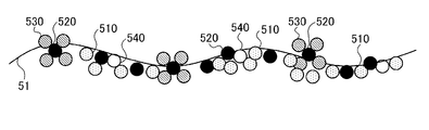
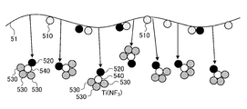
- 5A to 5C are diagrams showing a plasma processing model of the present embodiment.
- a molecular model group 510 indicates a model of carbon contained in the carbon-containing material attached to the electrode plate 51 after the wafer W is etched.
- a molecular model group 520 is a model of titanium contained in a titanium-containing material (for example, TiF 4 , TiN, TiO 2, Ti, etc.) attached to the electrode plate 51 after the wafer W is etched. Is shown.
- a molecular model group 530 indicates a model of fluorine contained in a titanium-containing material (for example, TiF 4 ) attached to the electrode plate 51 after the wafer W is etched.
- a molecular model group 540 represents a model of nitrogen contained in a titanium-containing material (for example, TiN) attached to the electrode plate 51 after the wafer W is etched.
- a molecular model group 550 indicates an oxygen model.
- a first fluorine-containing gas for example, C 4 F 8 gas
- the wafer W is etched using the plasma of the first fluorine-containing gas.
- Step 1 is executed.
- the carbon-containing material molecular model group 510
- the mask of the etched wafer W Titanium-containing materials molecular model group 520, molecular model group 530, and molecular model group 540 generated from the film adhere.
- the first step can be referred to as an “etching step”.
- O 2 gas is supplied to the plasma processing space S, and the carbon-containing material adhering to the electrode plate 51 after the first step is removed using the O 2 gas plasma.
- the second step is executed.
- the carbon-containing material on the surface of the electrode plate 51 and the O 2 gas plasma chemically react to become CO or CO 2 , and the carbon-containing material is removed from the surface of the electrode plate 51.
- the titanium-containing material on the surface of the electrode plate 51 is exposed.
- the second step can be called a “carbon-containing material removal step”.
- a nitrogen-containing gas for example, N 2 gas or NF 3 gas
- a second fluorine-containing gas for example, CF 4 gas, C 4 F 8 gas, or CHF 3 gas
- the third step of supplying and removing the titanium-containing material attached to the electrode plate 51 after the first step using the plasma of the nitrogen-containing gas and the second fluorine-containing gas is performed.
- the titanium-containing material on the surface of the electrode plate 51 chemically reacts with the plasma of the nitrogen-containing gas and the second fluorine-containing gas, and a complex gas such as Ti (NF 3 ) is produced. Occurs, and the titanium-containing material is removed from the surface of the electrode plate 51.
- the third step can be called a “titanium-containing material removal step”.
- the plasma processing and plasma processing apparatus 1 supplies the first fluorine-containing gas in the first step, and etches the wafer W using the first fluorine-containing gas. Then, the plasma processing and plasma processing apparatus 1 of the present embodiment supplies the O 2 gas to the plasma processing space S in the second step, and the carbon-containing material attached to the electrode plate 51 after the first step. By removing using O 2 gas plasma, the titanium-containing material on the surface of the electrode plate 51 is exposed. The plasma processing and plasma processing apparatus 1 of the present embodiment supplies the nitrogen-containing gas and the second fluorine-containing gas to the plasma processing space S in the third step, and performs the first step with respect to the electrode plate 51.
- the titanium-containing material attached later is removed using a plasma of a nitrogen-containing gas and a second fluorine-containing gas, thereby generating a complex gas such as Ti (NF 3 ).
- a complex gas such as Ti (NF 3 ).
- FIG. 6 is a flowchart of the plasma processing of the first embodiment.
- an etching process is executed (step S101). Specifically, the control unit 150 controls the flow rate adjustment mechanism 74 a to supply the first fluorine-containing gas to the plasma processing space S. Then, the controller 150 controls the first high-frequency power supply 30 and the second high-frequency power supply 40 to turn the first fluorine-containing gas into plasma, and the wafer W is formed using the plasma of the first fluorine-containing gas. Etch.
- a carbon-containing material removal step is executed (step S102). Specifically, the control unit 150 controls the flow rate adjustment mechanism 74 b to supply O 2 gas to the plasma processing space S. Then, the control unit 150 controls the first high-frequency power supply 30 and the second high-frequency power supply 40 to turn the O 2 gas into plasma, and to the electrode plate 51 disposed with the surface facing the plasma processing space S. The carbon-containing material adhering to the surface is removed using O 2 gas plasma.
- a titanium-containing material removal step is executed (step S103). Specifically, the control unit 150 controls the flow rate adjusting mechanism 74c and the flow rate adjusting mechanism 74d to supply the nitrogen-containing gas and the second fluorine-containing gas to the plasma processing space S. Then, the control unit 150 controls the first high-frequency power source 30 and the second high-frequency power source 40 to convert the nitrogen-containing gas and the second fluorine-containing gas into plasma, with the surface facing the plasma processing space S. The titanium-containing material attached to the arranged electrode plate 51 is removed using a nitrogen-containing gas and a second fluorine-containing gas.
- the etching process is performed to etch the wafer W, and then the carbon content removal process is performed to remove the carbon content adhering to the electrode plate 51 to remove the titanium content.
- the titanium-containing material can be removed as a complex gas such as Ti (NF 3 ) by exposing and then performing a titanium-containing material removing step. For this reason, even if deposits such as titanium-containing materials generated from the wafer W during etching adhere to the electrode plate 51, the titanium-containing materials can be efficiently removed from the deposits, so that plasma in the plasma processing space can be removed. It becomes possible to suppress fluctuations in density. As a result, variation with time in the etching characteristics of the wafer W can be suppressed.
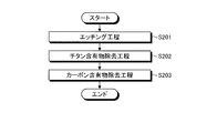
- FIG. 7 is a diagram showing a flowchart of the plasma processing of the second embodiment.
- an etching process is executed (step S201). Specifically, the control unit 150 controls the flow rate adjustment mechanism 74 a to supply the first fluorine-containing gas to the plasma processing space S. Then, the controller 150 controls the first high-frequency power supply 30 and the second high-frequency power supply 40 to turn the first fluorine-containing gas into plasma, and the wafer W is formed using the plasma of the first fluorine-containing gas. Etch.
- a titanium-containing material removal step is executed (step S202). Specifically, the control unit 150 controls the flow rate adjusting mechanism 74c and the flow rate adjusting mechanism 74d to supply the nitrogen-containing gas and the second fluorine-containing gas to the plasma processing space S. Then, the control unit 150 controls the first high-frequency power source 30 and the second high-frequency power source 40 to convert the nitrogen-containing gas and the second fluorine-containing gas into plasma, with the surface facing the plasma processing space S. The titanium-containing material attached to the arranged electrode plate 51 is removed using a nitrogen-containing gas and a second fluorine-containing gas.
- a carbon-containing material removal step is executed (step S203). Specifically, the control unit 150 controls the flow rate adjustment mechanism 74 b to supply O 2 gas to the plasma processing space S. Then, the control unit 150 controls the first high-frequency power supply 30 and the second high-frequency power supply 40 to turn the O 2 gas into plasma, and to the electrode plate 51 disposed with the surface facing the plasma processing space S. The carbon-containing material adhering to the surface is removed using O 2 gas plasma.
- the wafer W is etched by performing an etching process, and then the titanium-containing material attached to the electrode plate 51 is removed by performing a titanium-containing material removing process, such as Ti (NF 3 ).
- the carbon-containing material can be removed by removing it as a complex gas to expose the carbon-containing material and then performing a carbon-containing material removing step. For this reason, even if deposits such as titanium-containing materials generated from the wafer W during etching adhere to the electrode plate 51, carbon-containing materials among the deposits can be efficiently removed, so that plasma in the plasma processing space can be removed. It becomes possible to suppress fluctuations in density. As a result, variation with time in the etching characteristics of the wafer W can be suppressed.
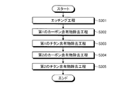
- FIG. 8 is a flowchart of the plasma processing according to the third embodiment.
- an etching process is executed (step S301). Specifically, the control unit 150 controls the flow rate adjustment mechanism 74 a to supply the first fluorine-containing gas to the plasma processing space S. Then, the controller 150 controls the first high-frequency power supply 30 and the second high-frequency power supply 40 to turn the first fluorine-containing gas into plasma, and the wafer W is formed using the plasma of the first fluorine-containing gas. Etch.
- a first carbon-containing material removal step is executed (step S302). Specifically, the control unit 150 controls the flow rate adjustment mechanism 74 b to supply O 2 gas to the plasma processing space S. Then, the control unit 150 controls the first high-frequency power supply 30 and the second high-frequency power supply 40 to turn the O 2 gas into plasma, and to the electrode plate 51 disposed with the surface facing the plasma processing space S. The carbon-containing material adhering to the surface is removed using O 2 gas plasma.
- a first titanium-containing material removal step is executed (step S303). Specifically, the control unit 150 controls the flow rate adjusting mechanism 74c and the flow rate adjusting mechanism 74d to supply the nitrogen-containing gas and the second fluorine-containing gas to the plasma processing space S. Then, the control unit 150 controls the first high-frequency power source 30 and the second high-frequency power source 40 to convert the nitrogen-containing gas and the second fluorine-containing gas into plasma, with the surface facing the plasma processing space S. The titanium-containing material attached to the arranged electrode plate 51 is removed using a nitrogen-containing gas and a second fluorine-containing gas.
- a second carbon-containing material removal step is executed (step S304). Specifically, the control unit 150 controls the flow rate adjustment mechanism 74 b to supply O 2 gas to the plasma processing space S. Then, the control unit 150 controls the first high-frequency power supply 30 and the second high-frequency power supply 40 to turn the O 2 gas into plasma, and to the electrode plate 51 disposed with the surface facing the plasma processing space S. The carbon-containing material adhering to the surface is removed using O 2 gas plasma.
- a second titanium-containing material removal step is executed (step S305). Specifically, the control unit 150 controls the flow rate adjusting mechanism 74c and the flow rate adjusting mechanism 74d to supply the nitrogen-containing gas and the second fluorine-containing gas to the plasma processing space S. Then, the control unit 150 controls the first high-frequency power source 30 and the second high-frequency power source 40 to convert the nitrogen-containing gas and the second fluorine-containing gas into plasma, with the surface facing the plasma processing space S. The titanium-containing material attached to the arranged electrode plate 51 is removed using a nitrogen-containing gas and a second fluorine-containing gas.
- the wafer W is etched by performing the etching step, and then the carbon-containing material attached to the electrode plate 51 by performing the carbon-containing material removing step.
- the titanium-containing material can be removed as a complex gas such as Ti (NF 3 ) by removing the titanium to expose the titanium-containing material and then performing a titanium-containing material removing step. For this reason, even if deposits such as titanium-containing materials generated from the wafer W during etching adhere to the electrode plate 51, the titanium-containing materials can be efficiently removed from the deposits, so that plasma in the plasma processing space can be removed. It becomes possible to suppress fluctuations in density. As a result, variation with time in the etching characteristics of the wafer W can be suppressed.
- the set of the carbon-containing material removal step and the titanium-containing material removal step is performed twice after the etching step is performed, so that the carbon plate adhered to the electrode plate 51. Deposits can be removed more efficiently.
- the set of the carbon-containing material removal step and the titanium-containing material removal step is repeated twice after the etching step is performed.
- the set of the removal step and the titanium-containing material removal step may be repeated twice or more.
- FIG. 9 is a view showing a flowchart of the plasma processing of the fourth embodiment.
- an etching process is executed (step S401). Specifically, the control unit 150 controls the flow rate adjustment mechanism 74 a to supply the first fluorine-containing gas to the plasma processing space S. Then, the controller 150 controls the first high-frequency power supply 30 and the second high-frequency power supply 40 to turn the first fluorine-containing gas into plasma, and the wafer W is formed using the plasma of the first fluorine-containing gas. Etch.
- a carbon-containing material removal step is executed (step S401). Specifically, the control unit 150 controls the flow rate adjustment mechanism 74 b to supply O 2 gas to the plasma processing space S. Then, the control unit 150 controls the first high-frequency power supply 30 and the second high-frequency power supply 40 to turn the O 2 gas into plasma, and to the electrode plate 51 disposed with the surface facing the plasma processing space S. The carbon-containing material adhering to the surface is removed using O 2 gas plasma.
- a titanium-containing material removal step using CHF 3 gas is executed (step S403).
- the control unit 150 controls the flow rate adjusting mechanism 74d and the like to supply CHF 3 gas to the plasma processing space S as the third fluorine-containing gas.
- the control unit 150 controls the first high-frequency power source 30 and the second high-frequency power source 40 to convert the CHF 3 gas into a plasma, and to the electrode plate 51 disposed with the surface facing the plasma processing space S.
- the titanium-containing material adhering thereto is removed using a plasma of CHF 3 gas.
- a titanium-containing material removal step is executed (step S404). Specifically, the control unit 150 controls the flow rate adjusting mechanism 74c and the flow rate adjusting mechanism 74d to supply the nitrogen-containing gas and the second fluorine-containing gas to the plasma processing space S. Then, the control unit 150 controls the first high-frequency power source 30 and the second high-frequency power source 40 to convert the nitrogen-containing gas and the second fluorine-containing gas into plasma, with the surface facing the plasma processing space S. The titanium-containing material attached to the arranged electrode plate 51 is removed using a nitrogen-containing gas and a second fluorine-containing gas.
- the wafer W is etched by performing the etching process, and then the carbon-containing material attached to the electrode plate 51 by performing the carbon-containing material removal process.
- the titanium-containing material can be removed as a complex gas such as Ti (NF 3 ) by removing the titanium to expose the titanium-containing material and then performing a titanium-containing material removing step. For this reason, even if deposits such as titanium-containing materials generated from the wafer W during etching adhere to the electrode plate 51, the titanium-containing materials can be efficiently removed from the deposits, so that plasma in the plasma processing space can be removed. It becomes possible to suppress fluctuations in density. As a result, variation with time in the etching characteristics of the wafer W can be suppressed.
- the CHF 3 gas as the third fluorine-containing gas is supplied to the plasma treatment space between the carbon-containing material removal step and the titanium-containing material removal step, and the electrode plate Since the titanium-containing material adhering to 51 is removed using the CHF 3 gas plasma, the adhering material adhering to the electrode plate 51 can be more efficiently removed.
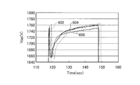
- FIG. 10A and FIG. 10B are views (No. 1) for explaining the effect of the plasma processing method of the present embodiment.
- 10A and 10B are diagrams showing effects when the plasma processing apparatus 1 performs the plasma processing on the wafer W.
- the horizontal axis indicates the time (sec) during which plasma processing is performed on the wafer W by the plasma processing apparatus 1
- the vertical axis indicates Vpp (V) of the wafer W.
- Vpp is a difference between the maximum value and the minimum value of the voltage value of the high frequency power on the surface of the wafer W. This Vpp is known to have a correlation with the plasma density due to the high frequency power, and the fluctuation of Vpp (V) can be said to be the fluctuation of the plasma density.
- FIG. 10A shows a lot number at the time of DC processing when dry cleaning (DC) processing using plasma of O 2 gas is performed on the wafer W without using the plasma processing method of the present embodiment. It is a graph which shows the relationship between Vpp of every wafer W, and time. That is, in FIG. 10A, a graph 602 shows Vpp and time when a trench for dual damascene wiring is etched (see FIG. 2) on 25 wafers W of lot number “1” and then DC processing is performed. Shows the relationship. A graph 604 shows the relationship between Vpp and time in DC processing after processing 25 wafers with lot number “2” (after processing 50 wafers in a cumulative manner including lot number “1”).
- a graph 606 shows the relationship between Vpp and time in DC processing after processing 25 wafers of lot number “3” (after processing of 75 wafers accumulated including lot numbers “1” and “2”).
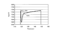
- FIG. 10B is a graph showing the relationship between the Vpp of the wafer W and the time for each lot number when the plasma processing is performed on the wafer W using the plasma processing method of the present embodiment. That is, in FIG. 10B, a graph 612 shows that after etching a groove for dual damascene wiring (see FIG. 2) on 25 wafers W of lot number “1”, the plasma processing of this embodiment is performed, and thereafter Shows the relationship between Vpp and time when DC processing is performed.
- the graph 612 is a diagram showing an effect when the plasma processing of the present embodiment is performed before the DC processing of FIG. 10A.
- Graph 614 shows the plasma processing of this embodiment after the processing of 25 wafers W of lot number “2” (after processing 50 wafers W including the lot number “1”), and Vpp in the subsequent DC processing.
- the graph 616 shows the relationship with time, after processing 25 wafers of lot number “3” (after processing of 75 wafers in a cumulative manner including lot numbers “1” and “2”). The relationship between Vpp and time in the subsequent DC processing is shown.
- the difference in the lot number causes the difference in Vpp of the wafer W as shown in graphs 602, 604, and 606.
- the history over time is different. This is presumably because the titanium-containing material generated from the mask film of the wafer W during etching accumulated on the electrode plate 51 facing the plasma processing space and the plasma density in the plasma processing space fluctuated.
- the carbon-containing material attached to the electrode plate 51 is removed by performing the carbon-containing material removing step.
- the titanium-containing material removal step By performing the titanium-containing material removal step, the titanium-containing material attached to the electrode plate 51 is removed.
- the history with respect to the time of Vpp of the wafer W is maintained equally regardless of the lot number. This is considered to be because the titanium-containing material adhering to the electrode plate 51 was removed even when the titanium-containing material generated from the mask film of the wafer W during etching adhered to the electrode plate 51 facing the plasma processing space. It is done. That is, it can be seen that fluctuations in plasma density are suppressed.
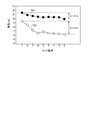
- FIG. 11 is a diagram (No. 2) for explaining the effect of the plasma processing method of the present embodiment.
- the horizontal axis indicates the lot number (accumulated value) of the wafer W carried into the plasma processing apparatus 1
- the vertical axis indicates a groove formed in the insulating film when the insulating film of the wafer W is etched.
- the groove diameter (nm) is shown.
- a graph 702 shows the lot diameter (accumulated value) of the groove diameter of the groove formed in the insulating film when only the DC treatment is performed without using the plasma treatment method of the present embodiment. It shows the fluctuation. Further, in FIG. 11, a graph 704 shows the variation of the groove diameter of the groove formed in the insulating film with respect to the lot number when the plasma processing method of the present embodiment is executed.
- the reduction width of the groove diameter formed in the insulating film with respect to the lot number is insulative when only the DC processing is executed.
- the groove diameter of the groove formed in the film is smaller than the reduction width with respect to the lot number.
Landscapes
- Chemical & Material Sciences (AREA)
- Engineering & Computer Science (AREA)
- Physics & Mathematics (AREA)
- Plasma & Fusion (AREA)
- Analytical Chemistry (AREA)
- Health & Medical Sciences (AREA)
- Public Health (AREA)
- Epidemiology (AREA)
- Materials Engineering (AREA)
- Mechanical Engineering (AREA)
- Metallurgy (AREA)
- Organic Chemistry (AREA)
- Drying Of Semiconductors (AREA)
- Plasma Technology (AREA)
Abstract
Description
11 処理容器
20 フォーカスリング
30 第1の高周波電源
40 第2の高周波電源
42 上部電極
51 電極板
52 電極支持体
72 処理ガス供給源
72a、72b、72c、72d ガス供給部
74a、74b、74c、74d 流量調整機構
150 制御部
D1 絶縁膜
D2 マスク膜
S プラズマ処理空間
W ウェハ
Claims (5)
- プラズマ処理装置におけるプラズマ処理方法であって、
第1のフッ素含有ガスをプラズマ処理空間に供給し、絶縁膜の表面にチタン含有物のマスク膜が形成された被処理基板を前記第1のフッ素含有ガスのプラズマを用いてエッチングする第1の工程と、
O2ガスを前記プラズマ処理空間に供給し、前記プラズマ処理空間に表面を対向させて配置された部材に対して前記第1の工程の後に付着したカーボン含有物を前記O2ガスのプラズマを用いて除去する第2の工程と、
窒素含有ガス及び第2のフッ素含有ガスを前記プラズマ処理空間に供給し、前記部材に対して前記第1の工程の後に付着したチタン含有物を前記窒素含有ガス及び前記第2のフッ素含有ガスのプラズマを用いて除去する第3の工程と
を含むことを特徴とするプラズマ処理方法。 - 前記第2の工程と前記第3の工程との間に、第3のフッ素含有ガスを前記プラズマ処理空間に供給し、前記部材に対して前記第1の工程の後に付着したチタン含有物を前記第3のフッ素含有ガスのプラズマを用いて除去する第4の工程をさらに含むことを特徴とする請求項1に記載のプラズマ処理方法。
- 前記プラズマ処理装置が、
前記第1の工程を実行した後に前記第2の工程及び前記第3の工程を少なくとも2回繰り返して実行することを特徴とする請求項1又は請求項2に記載のプラズマ処理方法。 - 前記窒素含有ガスは、N2ガス又はNF3ガスであり、前記第2のフッ素含有ガスは、CF4ガス、C4F8ガス又はCHF3ガスであることを特徴とする請求項1に記載のプラズマ処理方法。
- 絶縁膜の表面にチタン含有物のマスク膜が形成された被処理基板が配置されるプラズマ処理空間を画成する処理容器と、
第1のフッ素含有ガスを前記プラズマ処理空間に供給する第1のガス供給部と、
O2ガスを前記プラズマ処理空間に供給する第2のガス供給部と、
窒素含有ガス及び第2のフッ素含有ガスを前記プラズマ処理空間に供給する第3のガス供給部と、
前記第1のガス供給部から前記第1のフッ素含有ガスを前記プラズマ処理空間に供給し、前記第1のフッ素含有ガスのプラズマを用いて前記被処理基板をエッチングする第1の工程と、前記第2のガス供給部から前記O2ガスを前記プラズマ処理空間に供給し、前記プラズマ処理空間に表面を対向させて配置された部材に対して前記第1の工程の後に付着したカーボン含有物を前記O2ガスのプラズマを用いて除去する第2の工程と、前記第3のガス供給部から前記窒素含有ガス及び前記第2のフッ素含有ガスを前記プラズマ処理空間に供給し、前記部材に対して前記第1の工程の後に付着したチタン含有物を前記窒素含有ガス及び前記第2のフッ素含有ガスのプラズマを用いて除去する第3の工程とを実行する制御部と
を備えたことを特徴とするプラズマ処理装置。
Priority Applications (4)
| Application Number | Priority Date | Filing Date | Title |
|---|---|---|---|
| EP13833486.7A EP2879166B1 (en) | 2012-08-27 | 2013-08-07 | Plasma processing method |
| US14/424,217 US9460896B2 (en) | 2012-08-27 | 2013-08-07 | Plasma processing method and plasma processing apparatus |
| CN201380039947.7A CN104508803B (zh) | 2012-08-27 | 2013-08-07 | 等离子体处理方法 |
| KR1020157005120A KR102114922B1 (ko) | 2012-08-27 | 2013-08-07 | 플라즈마 처리 방법 |
Applications Claiming Priority (4)
| Application Number | Priority Date | Filing Date | Title |
|---|---|---|---|
| JP2012186344A JP5982223B2 (ja) | 2012-08-27 | 2012-08-27 | プラズマ処理方法、及びプラズマ処理装置 |
| JP2012-186344 | 2012-08-27 | ||
| US201261695630P | 2012-08-31 | 2012-08-31 | |
| US61/695,630 | 2012-08-31 |
Publications (1)
| Publication Number | Publication Date |
|---|---|
| WO2014034396A1 true WO2014034396A1 (ja) | 2014-03-06 |
Family
ID=50183214
Family Applications (1)
| Application Number | Title | Priority Date | Filing Date |
|---|---|---|---|
| PCT/JP2013/071409 Ceased WO2014034396A1 (ja) | 2012-08-27 | 2013-08-07 | プラズマ処理方法、及びプラズマ処理装置 |
Country Status (7)
| Country | Link |
|---|---|
| US (1) | US9460896B2 (ja) |
| EP (1) | EP2879166B1 (ja) |
| JP (1) | JP5982223B2 (ja) |
| KR (1) | KR102114922B1 (ja) |
| CN (1) | CN104508803B (ja) |
| TW (1) | TWI571930B (ja) |
| WO (1) | WO2014034396A1 (ja) |
Families Citing this family (10)
| Publication number | Priority date | Publication date | Assignee | Title |
|---|---|---|---|---|
| JP6049527B2 (ja) * | 2013-04-05 | 2016-12-21 | 東京エレクトロン株式会社 | プラズマ処理方法及びプラズマ処理装置 |
| JP2017045849A (ja) * | 2015-08-26 | 2017-03-02 | 東京エレクトロン株式会社 | シーズニング方法およびエッチング方法 |
| KR102729098B1 (ko) * | 2016-01-13 | 2024-11-13 | 어플라이드 머티어리얼스, 인코포레이티드 | 에칭 하드웨어를 위한 수소 플라즈마 기반 세정 프로세스 |
| CN107369603A (zh) * | 2016-05-12 | 2017-11-21 | 中芯国际集成电路制造(上海)有限公司 | 去除含氧副产物、清洗刻蚀腔和形成半导体结构的方法 |
| JP6785101B2 (ja) * | 2016-09-09 | 2020-11-18 | 東京エレクトロン株式会社 | プラズマエッチング方法 |
| JP6763750B2 (ja) * | 2016-11-07 | 2020-09-30 | 東京エレクトロン株式会社 | 被処理体を処理する方法 |
| JP6387198B1 (ja) * | 2017-04-14 | 2018-09-05 | 堺ディスプレイプロダクト株式会社 | 有機el表示装置の製造方法及び製造装置 |
| CN110637357A (zh) * | 2017-06-21 | 2019-12-31 | 惠普印迪格公司 | 真空工作台 |
| CN109962001A (zh) * | 2017-12-26 | 2019-07-02 | 中微半导体设备(上海)股份有限公司 | 一种等离子体腔室的运行方法和等离子反应器 |
| WO2023137275A1 (en) * | 2022-01-13 | 2023-07-20 | Lam Research Corporation | High selectivity and uniform dielectric etch |
Citations (7)
| Publication number | Priority date | Publication date | Assignee | Title |
|---|---|---|---|---|
| JPH03239323A (ja) * | 1990-02-16 | 1991-10-24 | Yamaha Corp | ドライエッチング方法 |
| JPH09171999A (ja) * | 1995-12-20 | 1997-06-30 | Hitachi Ltd | プラズマクリーニング処理方法 |
| JPH10280151A (ja) * | 1997-04-08 | 1998-10-20 | Fujitsu Ltd | Cvd装置のクリーニング方法 |
| JP2006035213A (ja) * | 2004-07-22 | 2006-02-09 | Air Products & Chemicals Inc | 窒化チタンの除去方法 |
| JP2006165246A (ja) * | 2004-12-07 | 2006-06-22 | Tokyo Electron Ltd | プラズマエッチング方法 |
| JP2006216964A (ja) | 2005-02-05 | 2006-08-17 | Samsung Electronics Co Ltd | ビアキャッピング保護膜を使用する半導体素子のデュアルダマシン配線の製造方法 |
| JP2012084600A (ja) * | 2010-10-07 | 2012-04-26 | Hitachi High-Technologies Corp | プラズマの処理方法及びプラズマ処理装置 |
Family Cites Families (9)
| Publication number | Priority date | Publication date | Assignee | Title |
|---|---|---|---|---|
| US5948702A (en) * | 1996-12-19 | 1999-09-07 | Texas Instruments Incorporated | Selective removal of TixNy |
| US6692903B2 (en) * | 2000-12-13 | 2004-02-17 | Applied Materials, Inc | Substrate cleaning apparatus and method |
| JP4176365B2 (ja) * | 2002-03-25 | 2008-11-05 | 東京エレクトロン株式会社 | プラズマエッチング方法 |
| US7488689B2 (en) * | 2004-12-07 | 2009-02-10 | Tokyo Electron Limited | Plasma etching method |
| JP4764028B2 (ja) * | 2005-02-28 | 2011-08-31 | 株式会社日立ハイテクノロジーズ | プラズマ処理方法 |
| JP4288252B2 (ja) * | 2005-04-19 | 2009-07-01 | パナソニック株式会社 | 半導体チップの製造方法 |
| JP2008198659A (ja) * | 2007-02-08 | 2008-08-28 | Tokyo Electron Ltd | プラズマエッチング方法 |
| US20120094499A1 (en) * | 2010-10-15 | 2012-04-19 | Siu Tang Ng | Method of performing an in situ chamber clean |
| JP6177601B2 (ja) * | 2013-06-25 | 2017-08-09 | 東京エレクトロン株式会社 | クリーニング方法及び基板処理装置 |
-
2012
- 2012-08-27 JP JP2012186344A patent/JP5982223B2/ja active Active
-
2013
- 2013-08-07 US US14/424,217 patent/US9460896B2/en active Active
- 2013-08-07 WO PCT/JP2013/071409 patent/WO2014034396A1/ja not_active Ceased
- 2013-08-07 CN CN201380039947.7A patent/CN104508803B/zh active Active
- 2013-08-07 KR KR1020157005120A patent/KR102114922B1/ko active Active
- 2013-08-07 EP EP13833486.7A patent/EP2879166B1/en active Active
- 2013-08-23 TW TW102130274A patent/TWI571930B/zh active
Patent Citations (7)
| Publication number | Priority date | Publication date | Assignee | Title |
|---|---|---|---|---|
| JPH03239323A (ja) * | 1990-02-16 | 1991-10-24 | Yamaha Corp | ドライエッチング方法 |
| JPH09171999A (ja) * | 1995-12-20 | 1997-06-30 | Hitachi Ltd | プラズマクリーニング処理方法 |
| JPH10280151A (ja) * | 1997-04-08 | 1998-10-20 | Fujitsu Ltd | Cvd装置のクリーニング方法 |
| JP2006035213A (ja) * | 2004-07-22 | 2006-02-09 | Air Products & Chemicals Inc | 窒化チタンの除去方法 |
| JP2006165246A (ja) * | 2004-12-07 | 2006-06-22 | Tokyo Electron Ltd | プラズマエッチング方法 |
| JP2006216964A (ja) | 2005-02-05 | 2006-08-17 | Samsung Electronics Co Ltd | ビアキャッピング保護膜を使用する半導体素子のデュアルダマシン配線の製造方法 |
| JP2012084600A (ja) * | 2010-10-07 | 2012-04-26 | Hitachi High-Technologies Corp | プラズマの処理方法及びプラズマ処理装置 |
Non-Patent Citations (1)
| Title |
|---|
| See also references of EP2879166A4 |
Also Published As
| Publication number | Publication date |
|---|---|
| TW201413817A (zh) | 2014-04-01 |
| EP2879166B1 (en) | 2019-10-09 |
| US9460896B2 (en) | 2016-10-04 |
| JP2014045063A (ja) | 2014-03-13 |
| TWI571930B (zh) | 2017-02-21 |
| JP5982223B2 (ja) | 2016-08-31 |
| EP2879166A1 (en) | 2015-06-03 |
| KR20150048134A (ko) | 2015-05-06 |
| CN104508803B (zh) | 2016-12-07 |
| EP2879166A4 (en) | 2016-03-16 |
| CN104508803A (zh) | 2015-04-08 |
| KR102114922B1 (ko) | 2020-05-25 |
| US20150228458A1 (en) | 2015-08-13 |
Similar Documents
| Publication | Publication Date | Title |
|---|---|---|
| JP5982223B2 (ja) | プラズマ処理方法、及びプラズマ処理装置 | |
| JP6211947B2 (ja) | 半導体装置の製造方法 | |
| JP6339963B2 (ja) | エッチング方法 | |
| JP2019207911A (ja) | 膜をエッチングする方法及びプラズマ処理装置 | |
| US11462412B2 (en) | Etching method | |
| US9818582B2 (en) | Plasma processing method | |
| JP2010140944A (ja) | プラズマエッチング装置及びプラズマクリーニング方法 | |
| JP6049527B2 (ja) | プラズマ処理方法及びプラズマ処理装置 | |
| JP6494424B2 (ja) | エッチング方法 | |
| JP6811202B2 (ja) | エッチングする方法及びプラズマ処理装置 | |
| JP7763251B2 (ja) | エッチング方法、半導体装置の製造方法、エッチングプログラムおよびプラズマ処理装置 | |
| US20160032445A1 (en) | Plasma processing apparatus and plasma processing method | |
| JP6063181B2 (ja) | プラズマ処理方法、及びプラズマ処理装置 | |
| WO2013191224A1 (ja) | シーズニング方法、プラズマ処理装置及び製造方法 | |
| JP2019117876A (ja) | エッチング方法 | |
| JP2006165246A (ja) | プラズマエッチング方法 | |
| CN111326395A (zh) | 等离子体处理方法和等离子体处理装置 | |
| TWI802266B (zh) | 蝕刻方法、半導體裝置之製造方法及電漿處理裝置 |
Legal Events
| Date | Code | Title | Description |
|---|---|---|---|
| 121 | Ep: the epo has been informed by wipo that ep was designated in this application |
Ref document number: 13833486 Country of ref document: EP Kind code of ref document: A1 |
|
| ENP | Entry into the national phase |
Ref document number: 20157005120 Country of ref document: KR Kind code of ref document: A |
|
| WWE | Wipo information: entry into national phase |
Ref document number: 14424217 Country of ref document: US |
|
| NENP | Non-entry into the national phase |
Ref country code: DE |
|
| WWE | Wipo information: entry into national phase |
Ref document number: 2013833486 Country of ref document: EP |