WO2014045341A1 - Élément optique, source lumineuse et affichage tête haute - Google Patents
Élément optique, source lumineuse et affichage tête haute Download PDFInfo
- Publication number
- WO2014045341A1 WO2014045341A1 PCT/JP2012/073837 JP2012073837W WO2014045341A1 WO 2014045341 A1 WO2014045341 A1 WO 2014045341A1 JP 2012073837 W JP2012073837 W JP 2012073837W WO 2014045341 A1 WO2014045341 A1 WO 2014045341A1
- Authority
- WO
- WIPO (PCT)
- Prior art keywords
- light
- microlens
- optical element
- light source
- screen
- Prior art date
- Legal status (The legal status is an assumption and is not a legal conclusion. Google has not performed a legal analysis and makes no representation as to the accuracy of the status listed.)
- Ceased
Links
Images








Classifications
-
- G—PHYSICS
- G02—OPTICS
- G02B—OPTICAL ELEMENTS, SYSTEMS OR APPARATUS
- G02B26/00—Optical devices or arrangements for the control of light using movable or deformable optical elements
- G02B26/08—Optical devices or arrangements for the control of light using movable or deformable optical elements for controlling the direction of light
- G02B26/10—Scanning systems
- G02B26/101—Scanning systems with both horizontal and vertical deflecting means, e.g. raster or XY scanners
-
- G—PHYSICS
- G02—OPTICS
- G02B—OPTICAL ELEMENTS, SYSTEMS OR APPARATUS
- G02B19/00—Condensers, e.g. light collectors or similar non-imaging optics
- G02B19/0004—Condensers, e.g. light collectors or similar non-imaging optics characterised by the optical means employed
- G02B19/0028—Condensers, e.g. light collectors or similar non-imaging optics characterised by the optical means employed refractive and reflective surfaces, e.g. non-imaging catadioptric systems
-
- G—PHYSICS
- G02—OPTICS
- G02B—OPTICAL ELEMENTS, SYSTEMS OR APPARATUS
- G02B19/00—Condensers, e.g. light collectors or similar non-imaging optics
- G02B19/0033—Condensers, e.g. light collectors or similar non-imaging optics characterised by the use
- G02B19/0047—Condensers, e.g. light collectors or similar non-imaging optics characterised by the use for use with a light source
-
- G—PHYSICS
- G02—OPTICS
- G02B—OPTICAL ELEMENTS, SYSTEMS OR APPARATUS
- G02B27/00—Optical systems or apparatus not provided for by any of the groups G02B1/00 - G02B26/00, G02B30/00
- G02B27/01—Head-up displays
- G02B27/0101—Head-up displays characterised by optical features
-
- G—PHYSICS
- G02—OPTICS
- G02B—OPTICAL ELEMENTS, SYSTEMS OR APPARATUS
- G02B3/00—Simple or compound lenses
- G02B3/0006—Arrays
-
- G—PHYSICS
- G02—OPTICS
- G02B—OPTICAL ELEMENTS, SYSTEMS OR APPARATUS
- G02B27/00—Optical systems or apparatus not provided for by any of the groups G02B1/00 - G02B26/00, G02B30/00
- G02B27/01—Head-up displays
- G02B27/0101—Head-up displays characterised by optical features
- G02B2027/0123—Head-up displays characterised by optical features comprising devices increasing the field of view
Definitions
- the present invention relates to a display technology using a microlens array.
- Patent Document 1 discloses a technique for generating an intermediate image using a dual lens array in which two microlens arrays are arranged to face each other at a predetermined distance.
- the dual lens array light that has passed through one lens array is collected by the other lens array and then emitted.
- the main object of the present invention is to provide an optical element, a light source unit, and a head-up display capable of suitably improving visibility.
- the optical element includes a microlens array unit in which a plurality of microlenses are arranged, and a reflection unit disposed to face the microlens array unit, and the microlens array unit The light that has passed through is reflected by the reflecting portion and then condensed on a microlens other than the incident microlens.
- FIG. 1 shows a schematic configuration of a head-up display. It is a block diagram which shows a part of light source unit. Sectional drawing along the incident direction of the light of a screen is shown. It is a front view of a reflective surface. It is the figure which showed a mode that light injects into a screen from a light source. It is a figure for demonstrating the method of determining the shape of a reflective surface from the mirror before a division
- the optical element includes a microlens array section in which a plurality of microlenses are arranged, and a reflection section disposed to face the microlens array section, and the microlens The light that has passed through the array part is reflected by the reflecting part and then condensed on a microlens other than the incident microlens.
- the above optical element includes a microlens array part and a reflection part.
- a plurality of microlenses are arranged in the microlens array section.
- the reflection part is disposed to face the microlens array part. Then, the light that has passed through the microlens array part is reflected by the reflecting part and then condensed on a microlens other than the incident microlens.
- the microlens that collects the light reflected by the reflection unit is a scanning direction of the optical element with respect to the microlens through which the light has passed before being reflected by the reflection unit. Alternatively, it exists at a position shifted by a predetermined number in the sub-scanning direction. According to this aspect, the optical element can suitably prevent the formation of a blind spot due to the light source while realizing high resolution.
- the microlens that collects the light reflected by the reflecting portion is shifted by the predetermined number from the microlens through which the light has passed before being reflected by the reflecting portion. It exists at a position that coincides with the vertical direction.
- the optical element can correct the reflection direction only in either the scanning direction or the sub-scanning direction, and simplify the position adjustment of the light source, the optical element, and the like.
- the light that has passed through the microlens array part is reflected by the reflecting part and then condensed on the main surface of the microlens where the reflected light is incident.
- the microlens array unit receives light emitted from a light source, and the light that has passed through the microlens array unit is reflected by the reflection unit and then enters the microlens. The light is condensed on the other microlens and emitted to the light source side.
- the optical element can reflect incident light in a direction different from the position where the light source exists, and suitably suppress the formation of a blind spot by the light source.
- the reflection unit has a positive power. According to this aspect, the reflection unit can preferably reflect the light that has passed through each microlens and collect the light on the same microlens.
- the reflecting portion is a mirror in which a mirror having a positive power is divided to reduce the thickness. According to this aspect, even if each microlens is formed on the same surface, the distance between the microlens array part and the reflecting part can be made almost constant regardless of the location, and the reflecting part is suitable. In addition, the light that has passed through each microlens can be reflected and condensed on another microlens.
- the microlens array unit and the reflection unit are integrally configured. According to this aspect, it is not necessary to align the microlens array portion and the reflecting portion, and the dual lens array can be simply configured, and a positional shift due to a change with time or the like does not occur.
- the optical element In another aspect of the optical element, light corresponding to one pixel is incident on each of the plurality of microlenses, and reflected light corresponding to the one pixel is condensed. According to this aspect, the optical element can suitably generate a high-resolution image.
- the optical element is a projector screen. Also according to this aspect, the optical element functions as a screen having a wide viewing angle while appropriately maintaining the luminance.
- the light source unit includes any one of the optical elements described above and a light source that emits light constituting a display image on the optical element.
- the light source unit is preferably applied to a head-up display, a head-mounted display, and the like.
- a light source unit can produce
- the light source is a laser scanning light source.
- the light source unit can allow the observer to visually recognize a high-resolution image while suppressing speckle noise.
- any one of the optical elements described above is provided, and an image formed by the optical element is visually recognized as a virtual image from the position of the user's eyes.
- the head-up display includes the above-described optical element, so that the viewer can clearly see the inner part of the display image on which relatively important information is displayed with high brightness, and the entire display image can be viewed by the viewer. Can be visually recognized.
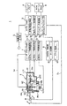
- FIG. 1 is a schematic configuration diagram of a head-up display according to the present embodiment.
- the head-up display according to the present embodiment is mounted on a vehicle and includes a light source 1, a screen 12 that is an intermediate image generating optical element, and a combiner 13.
- the light source 1 emits light constituting an intermediate image indicating information to be visually recognized by an observer toward the screen 12.
- the light source 1 is preferably a laser scanning light source. The specific configuration of the light source 1 will be described in detail in the section “Configuration of the light source”.
- the screen 12 is a reflective optical element that generates an intermediate image, and has a microlens array in which a plurality of microlenses are arranged.
- the specific configuration of the screen 12 will be described in the section [Screen Configuration].
- the combiner 13 is a half mirror that projects light constituting the intermediate image generated by the screen 12 and reflects the projected light to the driver's eye point “Pe”, thereby allowing the observer to visually recognize the virtual image. .
- the light source 1 and the screen 12 are preferably accommodated in the same casing.
- the light source 1 and the screen 12 are examples of the “light source unit” in the present invention.
- FIG. 2 is a configuration diagram showing a part of the light source 1.
- the light source 1 includes an image signal input unit 2, a video ASIC 3, a frame memory 4, a ROM 5, a RAM 6, a laser driver ASIC 7, a MEMS control unit 8, a laser light source unit 9, And a MEMS mirror 10.
- the image signal input unit 2 receives an image signal input from the outside and outputs it to the video ASIC 3.
- the video ASIC 3 is a block that controls the laser driver ASIC 7 and the MEMS control unit 8 based on the image signal input from the image signal input unit 2 and the scanning position information “Sc” input from the MEMS mirror 10, and the ASIC (Application) It is configured as Specific Integrated Circuit).
- the video ASIC 3 includes a synchronization / image separation unit 31, a bit data conversion unit 32, a light emission pattern conversion unit 33, and a timing controller 34.
- the synchronization / image separation unit 31 separates the image data displayed on the screen 12 serving as the image display unit and the synchronization signal from the image signal input from the image signal input unit 2, and writes the image data to the frame memory 4. .
- the bit data conversion unit 32 reads the image data written in the frame memory 4 and converts it into bit data.
- the light emission pattern conversion unit 33 converts the bit data converted by the bit data conversion unit 32 into a signal representing the light emission pattern of each laser.
- the timing controller 34 controls the operation timing of the synchronization / image separation unit 31 and the bit data conversion unit 32.
- the timing controller 34 also controls the operation timing of the MEMS control unit 8 described later.
- the image data separated by the synchronization / image separation unit 31 is written.
- the ROM 5 stores a control program and data for operating the video ASIC 3. Various data are sequentially read from and written into the RAM 6 as a work memory when the video ASIC 3 operates.
- the laser driver ASIC 7 is a block that generates a signal for driving a laser diode provided in a laser light source unit 9 described later, and is configured as an ASIC.
- the laser driver ASIC 7 includes a red laser driving circuit 71, a blue laser driving circuit 72, and a green laser driving circuit 73.
- the red laser driving circuit 71 drives the red laser LD1 based on the signal output from the light emission pattern conversion unit 33.
- the blue laser drive circuit 72 drives the blue laser LD2 based on the signal output from the light emission pattern conversion unit 33.
- the green laser drive circuit 73 drives the green laser LD3 based on the signal output from the light emission pattern conversion unit 33.
- the MEMS control unit 8 controls the MEMS mirror 10 based on a signal output from the timing controller 34.
- the MEMS control unit 8 includes a servo circuit 81 and a driver circuit 82.
- the servo circuit 81 controls the operation of the MEMS mirror 10 based on a signal from the timing controller.
- the driver circuit 82 amplifies the control signal of the MEMS mirror 10 output from the servo circuit 81 to a predetermined level and outputs the amplified signal.
- the laser light source unit 9 emits laser light to the MEMS mirror 10 based on the drive signal output from the laser driver ASIC 7.
- the MEMS mirror 10 as a scanning unit reflects the laser light emitted from the laser light source unit 9 toward the screen 12. In this way, the MEMS mirror 10 forms an image to be displayed on the screen 12.
- the MEMS mirror 10 moves so as to scan on the screen 12 under the control of the MEMS control unit 8 in order to display an image input to the image signal input unit 2, and the scanning position information (for example, information such as a mirror angle) is output to the video ASIC 3.
- the light source 1 causes the combiner 13 to reflect the light emitted from the screen 12 as described above, and causes the image corresponding to the reflected light to be visually recognized from the driver's eye point Pe as a virtual image.
- the laser light source unit 9 includes a case 91, a wavelength selective element 92, a collimator lens 93, a red laser LD 1, a blue laser LD 2, a green laser LD 3, and a monitor light receiving element (simply called “light receiving element”). 50).
- the case 91 is formed in a substantially box shape with resin or the like.
- the case 91 is provided with a hole penetrating into the case 91 and a CAN attachment portion 91a having a concave cross section, and a surface perpendicular to the CAN attachment portion 91a. A hole penetrating inward is formed, and a collimator mounting portion 91b having a concave cross section is formed.
- the wavelength-selective element 92 as a combining element is configured by, for example, a trichroic prism, and is provided with a reflective surface 92a and a reflective surface 92b.
- the reflection surface 92a transmits the laser light emitted from the red laser LD1 toward the collimator lens 93, and reflects the laser light emitted from the blue laser LD2 toward the collimator lens 93.
- the reflecting surface 92b transmits most of the laser light emitted from the red laser LD1 and the blue laser LD2 toward the collimator lens 93 and reflects a part thereof toward the light receiving element 50.
- the reflection surface 92 b reflects most of the laser light emitted from the green laser LD 3 toward the collimator lens 93 and transmits part of the laser light toward the light receiving element 50. In this way, the emitted light from each laser is superimposed and incident on the collimator lens 93 and the light receiving element 50.
- the wavelength selective element 92 is provided in the vicinity of the collimator mounting portion 91b in the case 91.
- the collimator lens 93 emits the laser beam incident from the wavelength selective element 92 to the MEMS mirror 10 as parallel light.
- the collimator lens 93 is fixed to the collimator mounting portion 91b of the case 91 with a UV adhesive or the like. That is, the collimator lens 93 is provided after the synthesis element.
- the red laser LD1 as a laser light source emits red laser light.
- the red laser LD1 is fixed at a position that is coaxial with the wavelength selective element 92 and the collimator lens 93 in the case 91 while the semiconductor laser light source is in the chip state or the chip is mounted on a submount or the like. ing.
- Blue laser LD2 as a laser light source emits blue laser light.
- the blue laser LD2 is fixed at a position where the emitted laser light can be reflected toward the collimator lens 93 by the reflecting surface 92a while the semiconductor laser light source is in the chip state or the chip is mounted on the submount or the like. ing.
- the positions of the red laser LD1 and the blue laser LD2 may be switched.
- the green laser LD3 as a laser light source is attached to the CAN package or attached to the frame package, and emits green laser light.
- the green laser LD 3 has a semiconductor laser light source chip B that generates green laser light in a CAN package, and is fixed to a CAN mounting portion 91 a of the case 91.
- the light receiving element 50 receives a part of the laser light emitted from each laser light source.
- the light receiving element 50 is a photoelectric conversion element such as a photodetector, and supplies a detection signal “Sd”, which is an electrical signal corresponding to the amount of incident laser light, to the laser driver ASIC 7.
- Sd a detection signal
- the laser driver ASIC 7 adjusts the power of the red laser LD1, the blue laser LD2, and the green laser LD3 according to the detection signal Sd.
- the laser driver ASIC 7 operates only the red laser driving circuit 71, supplies a driving current to the red laser LD1, and emits red laser light from the red laser LD1. A part of the red laser light is received by the light receiving element 50, and a detection signal Sd corresponding to the amount of light is fed back to the laser driver ASIC7.
- the laser driver ASIC 7 adjusts the drive current supplied from the red laser drive circuit 71 to the red laser LD1 so that the light amount indicated by the detection signal Sd is an appropriate light amount. In this way, power adjustment is performed.
- the power adjustment of the blue laser LD2 and the power adjustment of the green laser LD3 are similarly performed.
- FIG. 3 is a sectional view of the screen 12 according to the first embodiment.
- the direction perpendicular to the surface (microlens array 21 and reflection surface 22 described later) formed by the screen 12 is the “Z-axis direction”, and the direction perpendicular to the Z-axis direction in FIG.
- the main scanning direction of the emitted light is called the “Y-axis direction”, the Z-axis direction and the direction perpendicular to the Y-axis direction, and the sub-scanning direction of the emitted light from the light source 1 is called the “X-axis direction”. Is determined as shown in FIG. 3 and FIG. 4 described later.
- the screen 12 has a plate shape, and as shown in FIG. 3, a microlens array 21 is formed on a surface on which light from the light source 1 is incident, and the opposite side facing the microlens array 21.
- a reflective surface 22 is formed on the surface.
- the screen 12 is integrally formed from a transparent member so that the microlens array 21 and the reflection surface 22 are formed, and each surface is coded.
- the microlens array 21 has a plurality of microlenses 210 each having a regular hexagonal lens outline in plan view.
- the microlens 210 is formed in a lattice shape on the surface of the screen 12 on which light from the light source 1 is incident, and has an anti-reflection AR coating or the like.
- light corresponding to one pixel is incident on each microlens 210, and reflected light corresponding to one pixel is collected. Thereby, it is possible to prevent the resolution from being lowered and to achieve high definition.
- a mode in which light corresponding to one pixel is incident on the plurality of microlenses 210 and reflected light corresponding to one pixel is condensed may be used.
- the microlens array 21 functions as a “microlens array part” in the present invention.
- the reflective surface 22 functions as a mirror by applying a reflective coating or the like.
- the reflecting surface 22 has a shape in which a mirror having positive power is divided into concentric circular or elliptical regions to reduce the thickness, and has a cross section similar to that of a Fresnel lens.
- the mirror having the positive power described above is also referred to as “pre-division mirror Mb”.
- the pre-division mirror Mb is, for example, an elliptical mirror, a parabolic mirror, a toroidal mirror, or the like.
- the reflecting surface 22 functions as a “reflecting portion” in the present invention.
- FIG. 4 shows an example of a front view of the reflecting surface 22.
- the cut surface AB in FIG. 4 is observed from the direction of the arrow 15, it coincides with the sectional view of the screen 12 shown in FIG. 3.
- each of the divided regions is formed in a concentric circle or ellipse shape when viewed from the front.
- the reflection surface 22 has the same function as that of the pre-division mirror Mb, and reflects the light incident on each microlens 210 to each microlens 210 on which the light is incident. As a result, the reflected light of the light incident on each microlens 210 is collected on the main surface (incident surface) of each microlens 210. Further, since the reflection surface 22 has a shape in which the pre-division mirror Mb is divided and the thickness is reduced in the same manner as the Fresnel lens, the distance on the optical path between each microlens 210 and the reflection surface 22 is substantially constant.
- the reflecting surface 22 can preferably reflect the light that has passed through each microlens 210 and condense it on the same microlens 210.
- the specific distance between the microlens array 21 and the reflecting surface 22 is the distance that the light incident on each microlens 210 is collected on the main surface of each microlens 210 after being reflected by the reflecting surface 22. For example, it is set based on an experiment or the like.
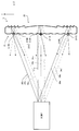
- FIG. 5 is a diagram schematically showing how light is emitted from the light source 1 to the screen 12.
- FIG. 5 shows the screen 12 in the same sectional view as FIG. 4 for convenience of explanation.
- the cross section of the screen 12 is not hatched.
- the light indicated by the light rays 31a to 31c is condensed at a condensing point 211A on the main surface of the microlens 210A to form pixels of an intermediate image.
- the light condensed at the condensing point 211 ⁇ / b> A is diffused toward the combiner 13 that exists in the negative Z-axis direction as in the light source 1.
- the light indicated by the light rays 32a to 32c having a larger incident angle on the screen 12 than the light indicated by the light rays 31a to 31c is incident on the microlens 210A, is reflected by the reflecting surface 22, and passes through the microlens 210A again.
- the light indicated by the light rays 32a to 32c is condensed at a condensing point 211B on the main surface of the microlens 210B to form pixels of an intermediate image.
- the light indicated by the light rays 34a to 34c having a larger incident angle on the screen 12 than the light indicated by the light rays 31a to 31c is incident on the microlens 210C, then reflected by the reflecting surface 22 and again passes through the microlens 210C. .
- the light indicated by the light beams 34a to 34c is condensed at a condensing point 211C on the main surface of the microlens 210C, and constitutes an intermediate image pixel.
- the reflecting surface 22 has the same function as the pre-division mirror Mb, the direction of the reflected light is appropriately directed toward the microlens 210A on which the light is incident even if the light has a large incident angle. to correct.
- the reflecting surface 22 is a flat surface, the light incident on the microlens 210 when the incident angle on the screen 12 exceeds a predetermined angle determined by the numerical aperture of the microlens 210 will be described. It is reflected by other microlenses 210 without being reflected toward the. In this case, the observer cannot properly visually recognize the entire display image.
- the reflecting surface 22 has a function equivalent to that of the undivided mirror Mb. Thereby, the light reflected by the reflecting surface 22 can be suitably condensed on the incident microlens 210 regardless of the numerical aperture of the microlens 210.
- FIG. 6A is a diagram in which an auxiliary line 16 for defining the shape of the reflection surface 22 is attached to the pre-division mirror Mb.
- the fragments 17a to 17j defined by the pre-division mirror Mb and the auxiliary line 16 extend in parallel or perpendicular to the Z axis so that the widths in the Z axis direction are the same.
- a broken line auxiliary line 16 is drawn.
- FIG. 6B is a diagram in which the pieces 17a to 17j are moved in the Z-axis direction so that the positions on the Z-axis coincide with each other. As shown in FIG.
- the reflecting surface 22 is formed along the surface of the fragments 17a to 17j on the Z axis negative direction side.
- the shape of the reflecting surface 22 can be determined from the pre-division mirror Mb.
- the pre-division mirror Mb is determined based on, for example, experiments so that the reflected light is corrected in a direction in which the reflected light is collected on the microlens 210 incident before the reflection.
- the luminance of the speckle noise in the case of a laser light source is suppressed as in the case of generating an intermediate image by the dual lens array in which the two lens arrays are arranged. Suppression and high resolution can be realized.
- the screen 12 of the present embodiment reflects the light that has passed through each microlens 210 and condenses the light again on the microlens 210 to generate an intermediate image. Accordingly, the screen 12 of this embodiment has the same optical characteristics except for the difference between the dual lens array and the reflective type or the transmissive type. Therefore, the configuration of the screen 12 can realize luminance unevenness suppression at an observation position, speckle noise suppression in the case of a laser scan type light source, and high resolution.
- the reflecting surface 22 has a function equivalent to that of the pre-division mirror Mb. Accordingly, as described with reference to FIG. 5, even when the incident angle to the microlens 210 is large due to the large projection angle, the reflecting surface 22 reflects the light to the incident microlens 210. To collect light.
- the screen 12 can expand the viewing angle while suppressing an increase in the diffuse reflection angle and a decrease in luminance.
- the distance between the light source 1 and the screen 12 can be shortened by the configuration of the screen 12, and the light source unit including the light source 1 and the screen 12 can be downsized.
- the light source and the screen are brought close to each other for the purpose of downsizing, it is necessary to increase the projection angle in order to maintain the irradiation range of the screen.
- the projection angle is increased, the luminance decreases due to an increase in the diffuse reflection angle on the screen.
- the reflecting surface 22 has a function equivalent to that of the pre-division mirror Mb, and reflects in the direction of the microlens 210 where the light is incident even when the incident angle of the light to the microlens 210 is large. Correct the direction of light.
- the screen 12 can appropriately generate an intermediate image while preventing a decrease in luminance.
- the screen 12 can easily align the microlens array 21 and the reflecting surface 22 as compared with the case where the two lenses are aligned in the dual lens array.
- the dual lens array is an optical element for generating an intermediate image
- the focal lengths of the pair of lenses described above are short, the influence on the position error is large and high-accuracy position adjustment is required. For this reason, when the dual lens array is an optical element for generating an intermediate image, an increase in labor during adjustment and a decrease in reliability due to a change with time are likely to occur.
- the focal length of the reflecting surface 22 is longer than that of the lens used for the lens array, so that the screen 12 is less susceptible to the positional shift on the XY plane than the dual lens array. .
- the reflecting surface 22 is axially symmetric or axially asymmetric, it is not easily affected by rotational deviation in the XY plane.
- the microlens 210 is regularly arranged and has a periodicity, the microlens array 21 is hardly affected by the pitch error as in the case of the dual lens array.
- each lens of one lens array and each lens of the other lens array need to be aligned in a pair, whereas the screen 12 has such alignment. There is no need.
- the screen 12 of this embodiment does not require high accuracy for alignment, including mold accuracy, so that it is possible to reduce the manufacturing cost and to have robustness and high reliability against changes with time.
- the viewing angle and the incident angle of light are limited by the numerical aperture of each microlens, whereas in the screen 12 according to the present embodiment, the viewing angle and the light Is not limited to the numerical aperture of each microlens 210.
- NA sin ( ⁇ / 2)
- NA the numerical aperture NA
- NA the numerical aperture NA
- NA the numerical aperture NA
- the diffusion angle ⁇ can be adjusted by designing each microlens so that the curvature of the microlens and the like become an appropriate value.
- the diffusion angle ⁇ can be reduced by increasing the curvature radius of each microlens, and the diffusion angle ⁇ can be increased by reducing the curvature radius of each microlens.
- the diffusion angle ⁇ has the same function as the viewing angle that is a performance index of a liquid crystal display or the like, and the smaller the diffusion angle ⁇ , the smaller the range (so-called eyebox) in which the portion of the corresponding display image can be visually recognized. .
- the larger the diffusion angle ⁇ the wider the range in which light diffuses, and the smaller the amount of light that reaches the eye point Pe.
- the incident angle of light exceeds an upper limit value corresponding to the numerical aperture NA of each microlens, the light incident on the lens of one dual lens array corresponds to the lens of the other dual lens array. And the observer cannot observe the entire image.
- the viewing angle and the luminance are in a trade-off relationship, and the incident angle of light is limited by the numerical aperture NA of each microlens.
- the screen 12 according to the present embodiment has an effect that the viewing angle can be widened without reducing the luminance, and the incident angle of light is not limited by the numerical aperture NA of each microlens.
- the screen 12 includes the microlens array 21 in which a plurality of microlenses 210 are arranged, and the reflective surface 22 that is disposed to face the microlens array 21.
- the light that has passed through the lens array 21 is reflected by the reflecting surface 22 and then condensed on the incident microlens 210.
- the screen 12 can reflect the light that has passed through each microlens and collect it on the same microlens. Therefore, as with the dual lens array, the screen 12 achieves high resolution and has uneven luminance at the observation point. Etc. can be reduced. Further, the screen 12 can realize a wide viewing angle while maintaining the luminance appropriately.
- Modification 1 In the first embodiment, substantially the entire surface of the screen 12 is irradiated with the emitted light from the light source 1.
- the configuration to which the present invention is applicable is not limited to this. Instead of this, the light emitted from the light source 1 may be applied to a part of the screen 12 and an arbitrary range. This will be described with reference to FIG.
- FIGS. 7A to 7C show examples of the irradiation range “RI” with respect to the reflection surface 22 of the screen 12. 7A to 7C, the position of the light source 1 with respect to the screen 12 is the same as in the first embodiment.
- the irradiation range RI is set to a quadrangle including the central portion of the reflecting surface 22.
- the reflecting surface 22 reflects and focuses the light on the microlens 210 on which the light is incident.
- the irradiation range RI is set higher than the example of FIG. 7A
- the irradiation range RI is set lower than the example of FIG. 7A. Is done.
- the reflecting surface 22 has a function equivalent to that of the pre-division mirror Mb, and therefore reflects and focuses the light on the microlens 210 on which the light is incident.
- the irradiation range RI when the irradiation range RI is fixed, only the region of the reflection surface 22 in the irradiation range RI out of the entire region of the reflection surface 22 may be designed to have a function equivalent to that of the pre-division mirror Mb. .
- the screen 12 may be obtained by cutting out the irradiation range RI shown in FIGS. 7A to 7C, and the reflection surface 22 other than the irradiation range RI shown in FIGS. You may form in a plane.
- the shape of the microlens 210 constituting the microlens array 21 is not limited to a regular hexagonal shape. This will be described with reference to FIG.
- FIG. 8A to 8E are diagrams in which microlenses 210 having respective shapes are arranged.
- the microlenses 210 have a regular hexagonal shape and are arranged in a lattice pattern.
- the micro lens 210 has a shape obtained by extending a regular hexagon in the Y-axis direction.
- the microlenses 210 have a square shape and are aligned in the X-axis direction and the Y-axis direction.
- FIG. 8D the microlens 210 has a square shape, and the rows arranged in the X-axis direction are alternately shifted in the Y-axis direction.
- a square has a shape extended in the X-axis direction, and the rows arranged in the X-axis direction are alternately shifted in the Y-axis direction.
- the shape of the microlens 210 is not limited to a regular hexagon, and an appropriate numerical aperture in the X-axis direction and Y-axis direction according to a required viewing angle in the X-axis direction and a viewing angle in the Y-axis direction. It is designed to have a numerical aperture of.
- FIG. 9A shows a cross-sectional view of the screen 12A on which the lens array layer 25 and the substrate layer 26 are provided.
- the shape of the reflection surface 22 is formed on one side of the substrate layer 26, and coating is performed by sputtering or the like.
- the lens array layer 25 in which the microlens array 21 is formed on the substrate layer 26 on which the reflection surface 22 is formed is transfer-molded by the 2P method or the like.
- FIG. 9B shows a cross-sectional view of the screen 12B in which the substrate layer 26 on which the reflecting surface 22 is formed and the lens array layer 25A are coupled by the low refractive index layer 28.
- a micro lens array 21A is formed on the lens array layer 25A so as to face the substrate layer 26.
- the low refractive index layer 28 has a lower refractive index than the lens array layer 25A. Also with this configuration, the light incident on the lens array layer 25A is reflected by the reflecting surface 22, and is condensed on the microlens 210 on which the light is incident.
- FIG. 10A shows a cross-sectional view of the screen 12C in which the reflecting surface 22 is a flat surface.
- FIG. 10B shows a cross-sectional view of the screen 12D in which the shape of the pre-division mirror Mb is made as it is without changing the shape of the reflection surface 22.
- a reflective surface 22B having the shape of the pre-division mirror Mb is formed on the substrate layer 26B.
- a lens array layer 25B in which microlenses 210 are arranged is formed along the reflecting surface 22B.
- the screen 12 ⁇ / b> D can suitably collect the light that has passed through the microlens 210 onto the incident microlens 210. Therefore, the screen 12D has the same effect as the screen 12 of the first embodiment.
- the application of the screen 12 is not limited to the head-up display, and may be used as a projector screen.
- FIG. 11 is a configuration example of a projection system having a light source (projector) 1 and a screen 12.
- the user emits light from the light source 1 to the screen 12 and visually recognizes a real image projected and displayed on the screen 12.
- the screen 12 can sufficiently increase the viewing angle and improve the visibility. Further, even when the distance between the screen 12 and the light source 1 is reduced, the user can preferably visually recognize the entire real image projected and displayed. Further, when the light source 1 is a laser scanning light source, the screen 12 can suitably suppress the generation of specific speckle noise.
- the screen 12 is suitably applied to a device that generates an intermediate image from a laser scan type light source, like a head-up display such as a head-mounted display. Even in this case, the screen 12 can suitably adjust the diffusion angle from the intermediate image and its direction as in the first embodiment.
- the configuration of the head-up display shown in FIG. 1 is an example, and the configuration to which the present invention is applicable is not limited to this.
- the head-up display does not have the combiner 13, and the light source 1 may reflect the display image on the front window to the driver's eye point Pe by projecting it onto the front window of the vehicle.
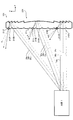
- FIG. 12 is a diagram showing a state in which light is incident on the screen 12X from the light source 1 in the second embodiment.
- FIG. 12 shows the screen 12 in section for convenience of explanation.
- the screen 12 ⁇ / b> X includes a microlens array 21 in which a plurality of microlenses 210 formed on a surface on which light from the light source 1 is incident, and the formation of the microlens array 21. And a reflective surface 22X formed on the opposite surface. Similar to the reflective surface 22 of the first embodiment, the reflective surface 22X functions as a mirror by a reflective coating and the like, and the pre-partition mirror Mb having a positive power is divided into concentric circular or elliptical regions to have a thickness. It has a reduced shape and a cross section similar to a Fresnel lens.
- the reflecting surface 22X reflects the light incident on each microlens 210 to the microlens 210 adjacent in the positive Y-axis direction of each microlens 210 on which the light is incident.
- the distance between the reflective surface 22X and the microlens array 21, the shape of the pre-division mirror Mb on which the reflective surface 22X functions, and the like are determined based on, for example, experiments.
- the light indicated by the light beams 34a to 34c emitted from the light source 1 and having an incident angle of approximately 0 is incident on the microlens 210C, then is reflected by the reflecting surface 22X, and passes through the microlens 210D adjacent to the microlens 210C in the positive Y-axis direction. pass.
- the light indicated by the light rays 34a to 34c is condensed at a condensing point 211D on the main surface of the microlens 210D, and constitutes an intermediate image pixel.
- the light condensed at the condensing point 211 ⁇ / b> D is emitted toward the combiner 13 that is closer to the Y-axis positive direction than the light source 1.
- the light indicated by the light rays 35a to 35c is incident on the microlens 210A at a larger incident angle than the light indicated by the light rays 34a to 34c, and then is reflected by the reflecting surface 22X and is adjacent to the microlens 210A in the Y axis positive direction. Pass through. At this time, the light indicated by the light rays 35a to 35c is condensed at a condensing point 211E on the main surface of the microlens 210E, and constitutes an intermediate image pixel.
- the reflecting surface 22X has a function equivalent to that of the pre-division mirror Mb even if the light has a large incident angle. Therefore, the microlens 210E adjacent to the microlens 210A on which the light has entered in the positive Y-axis direction. Correct the direction of the reflected light so that
- the light indicated by the light rays 36a to 36c is incident on the microlens 210B at a larger incident angle than the light indicated by the light rays 35a to 35c, and then is reflected by the reflecting surface 22X and is adjacent to the microlens 210B in the positive Y-axis direction. It passes through the micro lens 210F. At this time, the light indicated by the light rays 36a to 36c is condensed at a condensing point 211F on the main surface of the microlens 210F to constitute an intermediate image pixel.
- the reflecting surface 22X changes the direction of the reflected light so as to go to the microlens 210B where the light is incident and to the microlens 210F adjacent in the positive Y-axis direction regardless of the incident angle of the light to the microlens array 21. Correct appropriately.
- each microlens 210 the light incident on each microlens 210 is collected by the microlens 210 adjacent to the microlens 210 in the positive Y-axis direction to constitute each pixel of the intermediate image.
- the condensed light is emitted from the light source 1 in the positive direction of the Y axis. Therefore, since the light reflected by the screen 12X is emitted in a direction not overlapping the light source 1, no blind spot is formed by the light source 1.
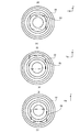
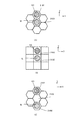
- FIGS. 13A to 13C the locations where the light emitted from the light source 1 is incident on the arranged microlenses 210 (also referred to as “incident spot SI”) and the reflected light from the reflecting surface 22X are collected. It is a figure which shows the positional relationship with the location (it is also called “injection spot SO”) which shines and inject
- regular hexagonal microlenses 210 are arranged in a lattice pattern.
- the microlens 210Y where the exit spot SO exists is present at a position adjacent to the microlens 210X where the incident spot SI exists in the positive direction of the Y axis.
- the square microlenses 210 are arranged in a state of being aligned in the X-axis direction and the Y-axis direction.
- the microlens 210V where the exit spot SO exists is present at a position adjacent to the microlens 210Z where the incident spot SI exists in the positive direction of the Y axis.
- FIG. 13A regular hexagonal microlenses 210 are arranged in a lattice pattern.
- the microlens 210Y where the exit spot SO exists is present at a position adjacent to the microlens 210X where the incident spot SI exists in the positive direction of the Y axis.
- regular hexagonal microlenses 210 are arranged in a lattice pattern.
- the microlens 210Y where the exit spot SO is present is present at the same position on the X axis as the microlens 210W where the incident spot SI is present, and is present at a position separated by the microlens 210X.
- the microlens 210 where the exit spot SO exists is equal to the predetermined number of microlenses 210 where the incident spot SI exists (1 in FIGS. 13A and 13B and 2 in FIG. 13C). It exists in the position away in the axial positive direction. By doing so, the reflection direction is corrected to the positive direction of the Y-axis on the reflection surface 22X so as to avoid the light source 1, and the light source 1 does not form a blind spot. Further, the microlens 210 where the exit spot SO exists is located at the same position on the X axis as the microlens 210 where the incident spot SI exists. By doing so, the reflected light from the screen 12X diffuses symmetrically with respect to the X-axis direction, so that the arrangement adjustment of the light source 1 and the screen 12X becomes easy.
- the screen 12X includes the microlens array 21 in which a plurality of microlenses 210 are arranged, and the reflection surface 22X arranged to face the microlens array 21.
- the light that has passed through the microlens array 21 is reflected by the reflecting surface 22X, and then condensed on the microlens 210 other than the incident microlens 210.
- the screen 12X can reflect light in the direction different from the light source 1 which is an incident direction, and it can suppress suitably that a blind spot is formed by the light source 1.
- Modification Next, a modified example suitable for the second embodiment will be described.
- Modifications 1 to 3 and Modification 5 of the first embodiment Modifications 6 and 7 described below can be applied in any combination.
- FIG. 14 is a configuration example of a projection system according to the second embodiment having a light source (projector) 1 and a screen 12X.
- the user emits light from the light source 1 to the screen 12X, and visually recognizes the real image projected and displayed on the screen 12X.
- the light emitted from the light source 1 is reflected by the screen 12X with the reflection direction corrected in the positive direction of the Y axis.
- the effect that the blind spot by the light source 1 is not formed is achieved, and the observer preferably displays the image projected and displayed on the screen 12X. It can be visually recognized.
- the microlens 210 where the exit spot SO exists is present at a position away from the microlens 210 where the incident spot SI exists by a predetermined number in the Y-axis positive direction.
- the configuration to which the present invention is applicable is not limited to this.
- the microlens 210 where the exit spot SO exists may exist at a position that is a predetermined number away from the microlens 210 where the incident spot SI exists in the Y-axis negative direction or the X-axis direction. This will be described with reference to FIG.
- FIG. 15A and 15B are diagrams showing the positional relationship between the incident spot SI and the exit spot SO in the modification.
- the microlens 210W where the exit spot SO exists coincides with the microlens 210X where the incident spot SI exists in the X-axis direction, and is present at a position adjacent to the Y-axis negative direction.
- the light reflected by the screen 12X passes through a position shifted in the negative Y-axis direction from the light source 1. Therefore, even in this case, a blind spot due to the light source 1 is not formed.
- the microlens 210H where the exit spot SO exists coincides with the microlens 210G where the incident spot SI exists in the Y-axis direction and is shifted by one in the negative X-axis direction. Exists in position. In this case, the light reflected by the screen 12X passes through a position shifted in the negative direction of the X axis from the light source 1. Accordingly, in this case, a blind spot due to the light source 1 is not formed.
- the microlens 210I in which the exit spot SO exists coincides with the microlens 210G in which the incident spot SI exists in the Y-axis direction and is one in the X-axis positive direction. It exists in the position shifted only. In this case, the light reflected by the screen 12X passes through a position shifted in the X axis positive direction from the light source 1. Therefore, also in this case, the blind spot by the light source 1 is not formed.
- the optical element according to the present invention can be suitably used for an optical element for generating an intermediate image used in a head-up display, a head-mounted display, or the like, a projector screen, or the like.
Landscapes
- Physics & Mathematics (AREA)
- General Physics & Mathematics (AREA)
- Optics & Photonics (AREA)
Priority Applications (1)
| Application Number | Priority Date | Filing Date | Title |
|---|---|---|---|
| PCT/JP2012/073837 WO2014045341A1 (fr) | 2012-09-18 | 2012-09-18 | Élément optique, source lumineuse et affichage tête haute |
Applications Claiming Priority (1)
| Application Number | Priority Date | Filing Date | Title |
|---|---|---|---|
| PCT/JP2012/073837 WO2014045341A1 (fr) | 2012-09-18 | 2012-09-18 | Élément optique, source lumineuse et affichage tête haute |
Publications (1)
| Publication Number | Publication Date |
|---|---|
| WO2014045341A1 true WO2014045341A1 (fr) | 2014-03-27 |
Family
ID=50340701
Family Applications (1)
| Application Number | Title | Priority Date | Filing Date |
|---|---|---|---|
| PCT/JP2012/073837 Ceased WO2014045341A1 (fr) | 2012-09-18 | 2012-09-18 | Élément optique, source lumineuse et affichage tête haute |
Country Status (1)
| Country | Link |
|---|---|
| WO (1) | WO2014045341A1 (fr) |
Cited By (2)
| Publication number | Priority date | Publication date | Assignee | Title |
|---|---|---|---|---|
| EP3035110A1 (fr) * | 2014-12-18 | 2016-06-22 | Optotune AG | Système optique permettant d'éviter la formation de motifs de taches |
| JP2016114738A (ja) * | 2014-12-15 | 2016-06-23 | セイコーエプソン株式会社 | プロジェクター |
Citations (3)
| Publication number | Priority date | Publication date | Assignee | Title |
|---|---|---|---|---|
| US20100079861A1 (en) * | 2008-09-29 | 2010-04-01 | Microvision, Inc. | Exit Pupil Forming Scanned Beam Projection Display Having Higher Uniformity |
| JP2010145745A (ja) * | 2008-12-18 | 2010-07-01 | Equos Research Co Ltd | 画像形成装置、及び、ヘッドアップディスプレイ装置 |
| WO2012042744A1 (fr) * | 2010-10-01 | 2012-04-05 | パナソニック株式会社 | Dispositif d'affichage, corps mobile et dispositif de commande |
-
2012
- 2012-09-18 WO PCT/JP2012/073837 patent/WO2014045341A1/fr not_active Ceased
Patent Citations (3)
| Publication number | Priority date | Publication date | Assignee | Title |
|---|---|---|---|---|
| US20100079861A1 (en) * | 2008-09-29 | 2010-04-01 | Microvision, Inc. | Exit Pupil Forming Scanned Beam Projection Display Having Higher Uniformity |
| JP2010145745A (ja) * | 2008-12-18 | 2010-07-01 | Equos Research Co Ltd | 画像形成装置、及び、ヘッドアップディスプレイ装置 |
| WO2012042744A1 (fr) * | 2010-10-01 | 2012-04-05 | パナソニック株式会社 | Dispositif d'affichage, corps mobile et dispositif de commande |
Cited By (2)
| Publication number | Priority date | Publication date | Assignee | Title |
|---|---|---|---|---|
| JP2016114738A (ja) * | 2014-12-15 | 2016-06-23 | セイコーエプソン株式会社 | プロジェクター |
| EP3035110A1 (fr) * | 2014-12-18 | 2016-06-22 | Optotune AG | Système optique permettant d'éviter la formation de motifs de taches |
Similar Documents
| Publication | Publication Date | Title |
|---|---|---|
| US8422137B2 (en) | Optical element, head-up display and method for producing optical element | |
| JP5732969B2 (ja) | ヘッドアップディスプレイ装置 | |
| EP3447561B1 (fr) | Dispositif d'affichage tête haute | |
| JP6696236B2 (ja) | 表示装置および導光装置 | |
| CN104345409B (zh) | 波分复用传输装置的制造方法、波分复用传输装置 | |
| US20150070770A1 (en) | Optical element, head-up display and light source unit | |
| KR102519000B1 (ko) | 화상 표시장치 | |
| US9903987B2 (en) | Laser optical device and image projection device | |
| JP5021850B1 (ja) | 光源ユニット及びヘッドアップディスプレイ | |
| TWI766954B (zh) | 分裂出射瞳孔抬頭顯示系統及方法 | |
| KR20170047271A (ko) | 스플릿 사출 동공 헤드업 디스플레이 시스템 및 방법 | |
| KR102664690B1 (ko) | 비대칭 프리즘을 구비한 차량용 헤드업 디스플레이 장치 | |
| JP6606998B2 (ja) | スクリーン、画像表示装置及び物体装置 | |
| JP2018036501A (ja) | 虚像表示装置 | |
| WO2012140766A1 (fr) | Élément optique, dispositif d'affichage tête-haute, et unité de source de lumière | |
| JP5837685B2 (ja) | 光源ユニット及びヘッドアップディスプレイ | |
| JP2012226304A (ja) | ヘッドアップディスプレイ | |
| WO2014045340A1 (fr) | Élément optique, source lumineuse et affichage tête haute | |
| WO2013179493A1 (fr) | Appareil de projection d'image, dispositif d'affichage tête haute, procédé de commande et élément optique | |
| WO2014045341A1 (fr) | Élément optique, source lumineuse et affichage tête haute | |
| JP2018036499A (ja) | 虚像表示装置 | |
| JP2015219389A (ja) | 虚像表示装置及び画像形成素子 | |
| WO2013179494A1 (fr) | Dispositif de projection, dispositif d'affichage tête haute, procédé de commande, programme et support de stockage | |
| JP6515616B2 (ja) | プロジェクター | |
| JP2006047804A (ja) | 光走査装置及び画像表示装置 |
Legal Events
| Date | Code | Title | Description |
|---|---|---|---|
| 121 | Ep: the epo has been informed by wipo that ep was designated in this application |
Ref document number: 12884999 Country of ref document: EP Kind code of ref document: A1 |
|
| NENP | Non-entry into the national phase |
Ref country code: DE |
|
| 122 | Ep: pct application non-entry in european phase |
Ref document number: 12884999 Country of ref document: EP Kind code of ref document: A1 |
|
| NENP | Non-entry into the national phase |
Ref country code: JP |