WO2014045842A1 - 半導体装置 - Google Patents
半導体装置 Download PDFInfo
- Publication number
- WO2014045842A1 WO2014045842A1 PCT/JP2013/073335 JP2013073335W WO2014045842A1 WO 2014045842 A1 WO2014045842 A1 WO 2014045842A1 JP 2013073335 W JP2013073335 W JP 2013073335W WO 2014045842 A1 WO2014045842 A1 WO 2014045842A1
- Authority
- WO
- WIPO (PCT)
- Prior art keywords
- electrode
- fet
- diode
- wiring pattern
- semiconductor device
- Prior art date
- Legal status (The legal status is an assumption and is not a legal conclusion. Google has not performed a legal analysis and makes no representation as to the accuracy of the status listed.)
- Ceased
Links
Images








Classifications
-
- H—ELECTRICITY
- H10—SEMICONDUCTOR DEVICES; ELECTRIC SOLID-STATE DEVICES NOT OTHERWISE PROVIDED FOR
- H10W—GENERIC PACKAGES, INTERCONNECTIONS, CONNECTORS OR OTHER CONSTRUCTIONAL DETAILS OF DEVICES COVERED BY CLASS H10
- H10W90/00—Package configurations
-
- H—ELECTRICITY
- H10—SEMICONDUCTOR DEVICES; ELECTRIC SOLID-STATE DEVICES NOT OTHERWISE PROVIDED FOR
- H10D—INORGANIC ELECTRIC SEMICONDUCTOR DEVICES
- H10D12/00—Bipolar devices controlled by the field effect, e.g. insulated-gate bipolar transistors [IGBT]
- H10D12/411—Insulated-gate bipolar transistors [IGBT]
- H10D12/441—Vertical IGBTs
-
- H—ELECTRICITY
- H10—SEMICONDUCTOR DEVICES; ELECTRIC SOLID-STATE DEVICES NOT OTHERWISE PROVIDED FOR
- H10D—INORGANIC ELECTRIC SEMICONDUCTOR DEVICES
- H10D30/00—Field-effect transistors [FET]
- H10D30/60—Insulated-gate field-effect transistors [IGFET]
- H10D30/63—Vertical IGFETs
-
- H—ELECTRICITY
- H10—SEMICONDUCTOR DEVICES; ELECTRIC SOLID-STATE DEVICES NOT OTHERWISE PROVIDED FOR
- H10D—INORGANIC ELECTRIC SEMICONDUCTOR DEVICES
- H10D8/00—Diodes
-
- H—ELECTRICITY
- H10—SEMICONDUCTOR DEVICES; ELECTRIC SOLID-STATE DEVICES NOT OTHERWISE PROVIDED FOR
- H10W—GENERIC PACKAGES, INTERCONNECTIONS, CONNECTORS OR OTHER CONSTRUCTIONAL DETAILS OF DEVICES COVERED BY CLASS H10
- H10W20/00—Interconnections in chips, wafers or substrates
- H10W20/40—Interconnections external to wafers or substrates, e.g. back-end-of-line [BEOL] metallisations or vias connecting to gate electrodes
- H10W20/41—Interconnections external to wafers or substrates, e.g. back-end-of-line [BEOL] metallisations or vias connecting to gate electrodes characterised by their conductive parts
- H10W20/43—Layouts of interconnections
-
- H—ELECTRICITY
- H10—SEMICONDUCTOR DEVICES; ELECTRIC SOLID-STATE DEVICES NOT OTHERWISE PROVIDED FOR
- H10W—GENERIC PACKAGES, INTERCONNECTIONS, CONNECTORS OR OTHER CONSTRUCTIONAL DETAILS OF DEVICES COVERED BY CLASS H10
- H10W40/00—Arrangements for thermal protection or thermal control
- H10W40/20—Arrangements for cooling
- H10W40/22—Arrangements for cooling characterised by their shape, e.g. having conical or cylindrical projections
-
- H—ELECTRICITY
- H10—SEMICONDUCTOR DEVICES; ELECTRIC SOLID-STATE DEVICES NOT OTHERWISE PROVIDED FOR
- H10W—GENERIC PACKAGES, INTERCONNECTIONS, CONNECTORS OR OTHER CONSTRUCTIONAL DETAILS OF DEVICES COVERED BY CLASS H10
- H10W40/00—Arrangements for thermal protection or thermal control
- H10W40/70—Fillings or auxiliary members in containers or in encapsulations for thermal protection or control
- H10W40/77—Auxiliary members characterised by their shape
- H10W40/778—Auxiliary members characterised by their shape in encapsulations
-
- H—ELECTRICITY
- H10—SEMICONDUCTOR DEVICES; ELECTRIC SOLID-STATE DEVICES NOT OTHERWISE PROVIDED FOR
- H10W—GENERIC PACKAGES, INTERCONNECTIONS, CONNECTORS OR OTHER CONSTRUCTIONAL DETAILS OF DEVICES COVERED BY CLASS H10
- H10W70/00—Package substrates; Interposers; Redistribution layers [RDL]
- H10W70/40—Leadframes
- H10W70/451—Multilayered leadframes
-
- H—ELECTRICITY
- H10—SEMICONDUCTOR DEVICES; ELECTRIC SOLID-STATE DEVICES NOT OTHERWISE PROVIDED FOR
- H10W—GENERIC PACKAGES, INTERCONNECTIONS, CONNECTORS OR OTHER CONSTRUCTIONAL DETAILS OF DEVICES COVERED BY CLASS H10
- H10W70/00—Package substrates; Interposers; Redistribution layers [RDL]
- H10W70/40—Leadframes
- H10W70/464—Additional interconnections in combination with leadframes
- H10W70/466—Tape carriers or flat leads
-
- H—ELECTRICITY
- H10—SEMICONDUCTOR DEVICES; ELECTRIC SOLID-STATE DEVICES NOT OTHERWISE PROVIDED FOR
- H10W—GENERIC PACKAGES, INTERCONNECTIONS, CONNECTORS OR OTHER CONSTRUCTIONAL DETAILS OF DEVICES COVERED BY CLASS H10
- H10W70/00—Package substrates; Interposers; Redistribution layers [RDL]
- H10W70/40—Leadframes
- H10W70/481—Leadframes for devices being provided for in groups H10D8/00 - H10D48/00
-
- H—ELECTRICITY
- H10—SEMICONDUCTOR DEVICES; ELECTRIC SOLID-STATE DEVICES NOT OTHERWISE PROVIDED FOR
- H10W—GENERIC PACKAGES, INTERCONNECTIONS, CONNECTORS OR OTHER CONSTRUCTIONAL DETAILS OF DEVICES COVERED BY CLASS H10
- H10W70/00—Package substrates; Interposers; Redistribution layers [RDL]
- H10W70/60—Insulating or insulated package substrates; Interposers; Redistribution layers
- H10W70/62—Insulating or insulated package substrates; Interposers; Redistribution layers characterised by their interconnections
- H10W70/65—Shapes or dispositions of interconnections
- H10W70/658—Shapes or dispositions of interconnections for devices provided for in groups H10D8/00 - H10D48/00
-
- H—ELECTRICITY
- H10—SEMICONDUCTOR DEVICES; ELECTRIC SOLID-STATE DEVICES NOT OTHERWISE PROVIDED FOR
- H10W—GENERIC PACKAGES, INTERCONNECTIONS, CONNECTORS OR OTHER CONSTRUCTIONAL DETAILS OF DEVICES COVERED BY CLASS H10
- H10W72/00—Interconnections or connectors in packages
- H10W72/60—Strap connectors, e.g. thick copper clips for grounding of power devices
-
- H—ELECTRICITY
- H10—SEMICONDUCTOR DEVICES; ELECTRIC SOLID-STATE DEVICES NOT OTHERWISE PROVIDED FOR
- H10W—GENERIC PACKAGES, INTERCONNECTIONS, CONNECTORS OR OTHER CONSTRUCTIONAL DETAILS OF DEVICES COVERED BY CLASS H10
- H10W74/00—Encapsulations, e.g. protective coatings
- H10W74/10—Encapsulations, e.g. protective coatings characterised by their shape or disposition
- H10W74/111—Encapsulations, e.g. protective coatings characterised by their shape or disposition the semiconductor body being completely enclosed
-
- H—ELECTRICITY
- H10—SEMICONDUCTOR DEVICES; ELECTRIC SOLID-STATE DEVICES NOT OTHERWISE PROVIDED FOR
- H10W—GENERIC PACKAGES, INTERCONNECTIONS, CONNECTORS OR OTHER CONSTRUCTIONAL DETAILS OF DEVICES COVERED BY CLASS H10
- H10W90/00—Package configurations
- H10W90/811—Multiple chips on leadframes
-
- H—ELECTRICITY
- H10—SEMICONDUCTOR DEVICES; ELECTRIC SOLID-STATE DEVICES NOT OTHERWISE PROVIDED FOR
- H10D—INORGANIC ELECTRIC SEMICONDUCTOR DEVICES
- H10D30/00—Field-effect transistors [FET]
- H10D30/60—Insulated-gate field-effect transistors [IGFET]
- H10D30/64—Double-diffused metal-oxide semiconductor [DMOS] FETs
- H10D30/66—Vertical DMOS [VDMOS] FETs
-
- H—ELECTRICITY
- H10—SEMICONDUCTOR DEVICES; ELECTRIC SOLID-STATE DEVICES NOT OTHERWISE PROVIDED FOR
- H10W—GENERIC PACKAGES, INTERCONNECTIONS, CONNECTORS OR OTHER CONSTRUCTIONAL DETAILS OF DEVICES COVERED BY CLASS H10
- H10W70/00—Package substrates; Interposers; Redistribution layers [RDL]
- H10W70/60—Insulating or insulated package substrates; Interposers; Redistribution layers
- H10W70/62—Insulating or insulated package substrates; Interposers; Redistribution layers characterised by their interconnections
- H10W70/65—Shapes or dispositions of interconnections
-
- H—ELECTRICITY
- H10—SEMICONDUCTOR DEVICES; ELECTRIC SOLID-STATE DEVICES NOT OTHERWISE PROVIDED FOR
- H10W—GENERIC PACKAGES, INTERCONNECTIONS, CONNECTORS OR OTHER CONSTRUCTIONAL DETAILS OF DEVICES COVERED BY CLASS H10
- H10W70/00—Package substrates; Interposers; Redistribution layers [RDL]
- H10W70/60—Insulating or insulated package substrates; Interposers; Redistribution layers
- H10W70/67—Insulating or insulated package substrates; Interposers; Redistribution layers characterised by their insulating layers or insulating parts
- H10W70/68—Shapes or dispositions thereof
- H10W70/682—Shapes or dispositions thereof comprising holes having chips therein
-
- H—ELECTRICITY
- H10—SEMICONDUCTOR DEVICES; ELECTRIC SOLID-STATE DEVICES NOT OTHERWISE PROVIDED FOR
- H10W—GENERIC PACKAGES, INTERCONNECTIONS, CONNECTORS OR OTHER CONSTRUCTIONAL DETAILS OF DEVICES COVERED BY CLASS H10
- H10W72/00—Interconnections or connectors in packages
- H10W72/071—Connecting or disconnecting
- H10W72/073—Connecting or disconnecting of die-attach connectors
- H10W72/07321—Aligning
- H10W72/07327—Aligning involving guiding structures, e.g. spacers or supporting members
-
- H—ELECTRICITY
- H10—SEMICONDUCTOR DEVICES; ELECTRIC SOLID-STATE DEVICES NOT OTHERWISE PROVIDED FOR
- H10W—GENERIC PACKAGES, INTERCONNECTIONS, CONNECTORS OR OTHER CONSTRUCTIONAL DETAILS OF DEVICES COVERED BY CLASS H10
- H10W72/00—Interconnections or connectors in packages
- H10W72/071—Connecting or disconnecting
- H10W72/073—Connecting or disconnecting of die-attach connectors
- H10W72/07331—Connecting techniques
-
- H—ELECTRICITY
- H10—SEMICONDUCTOR DEVICES; ELECTRIC SOLID-STATE DEVICES NOT OTHERWISE PROVIDED FOR
- H10W—GENERIC PACKAGES, INTERCONNECTIONS, CONNECTORS OR OTHER CONSTRUCTIONAL DETAILS OF DEVICES COVERED BY CLASS H10
- H10W72/00—Interconnections or connectors in packages
- H10W72/071—Connecting or disconnecting
- H10W72/073—Connecting or disconnecting of die-attach connectors
- H10W72/07331—Connecting techniques
- H10W72/07336—Soldering or alloying
-
- H—ELECTRICITY
- H10—SEMICONDUCTOR DEVICES; ELECTRIC SOLID-STATE DEVICES NOT OTHERWISE PROVIDED FOR
- H10W—GENERIC PACKAGES, INTERCONNECTIONS, CONNECTORS OR OTHER CONSTRUCTIONAL DETAILS OF DEVICES COVERED BY CLASS H10
- H10W72/00—Interconnections or connectors in packages
- H10W72/071—Connecting or disconnecting
- H10W72/073—Connecting or disconnecting of die-attach connectors
- H10W72/07351—Connecting or disconnecting of die-attach connectors characterised by changes in properties of the die-attach connectors during connecting
- H10W72/07354—Connecting or disconnecting of die-attach connectors characterised by changes in properties of the die-attach connectors during connecting changes in dispositions
-
- H—ELECTRICITY
- H10—SEMICONDUCTOR DEVICES; ELECTRIC SOLID-STATE DEVICES NOT OTHERWISE PROVIDED FOR
- H10W—GENERIC PACKAGES, INTERCONNECTIONS, CONNECTORS OR OTHER CONSTRUCTIONAL DETAILS OF DEVICES COVERED BY CLASS H10
- H10W72/00—Interconnections or connectors in packages
- H10W72/071—Connecting or disconnecting
- H10W72/076—Connecting or disconnecting of strap connectors
- H10W72/07651—Connecting or disconnecting of strap connectors characterised by changes in properties of the strap connectors during connecting
- H10W72/07653—Connecting or disconnecting of strap connectors characterised by changes in properties of the strap connectors during connecting changes in shapes
-
- H—ELECTRICITY
- H10—SEMICONDUCTOR DEVICES; ELECTRIC SOLID-STATE DEVICES NOT OTHERWISE PROVIDED FOR
- H10W—GENERIC PACKAGES, INTERCONNECTIONS, CONNECTORS OR OTHER CONSTRUCTIONAL DETAILS OF DEVICES COVERED BY CLASS H10
- H10W72/00—Interconnections or connectors in packages
- H10W72/30—Die-attach connectors
- H10W72/321—Structures or relative sizes of die-attach connectors
- H10W72/325—Die-attach connectors having a filler embedded in a matrix
-
- H—ELECTRICITY
- H10—SEMICONDUCTOR DEVICES; ELECTRIC SOLID-STATE DEVICES NOT OTHERWISE PROVIDED FOR
- H10W—GENERIC PACKAGES, INTERCONNECTIONS, CONNECTORS OR OTHER CONSTRUCTIONAL DETAILS OF DEVICES COVERED BY CLASS H10
- H10W72/00—Interconnections or connectors in packages
- H10W72/30—Die-attach connectors
- H10W72/341—Dispositions of die-attach connectors, e.g. layouts
- H10W72/347—Dispositions of multiple die-attach connectors
-
- H—ELECTRICITY
- H10—SEMICONDUCTOR DEVICES; ELECTRIC SOLID-STATE DEVICES NOT OTHERWISE PROVIDED FOR
- H10W—GENERIC PACKAGES, INTERCONNECTIONS, CONNECTORS OR OTHER CONSTRUCTIONAL DETAILS OF DEVICES COVERED BY CLASS H10
- H10W72/00—Interconnections or connectors in packages
- H10W72/30—Die-attach connectors
- H10W72/351—Materials of die-attach connectors
- H10W72/352—Materials of die-attach connectors comprising metals or metalloids, e.g. solders
-
- H—ELECTRICITY
- H10—SEMICONDUCTOR DEVICES; ELECTRIC SOLID-STATE DEVICES NOT OTHERWISE PROVIDED FOR
- H10W—GENERIC PACKAGES, INTERCONNECTIONS, CONNECTORS OR OTHER CONSTRUCTIONAL DETAILS OF DEVICES COVERED BY CLASS H10
- H10W72/00—Interconnections or connectors in packages
- H10W72/30—Die-attach connectors
- H10W72/351—Materials of die-attach connectors
- H10W72/353—Materials of die-attach connectors not comprising solid metals or solid metalloids, e.g. ceramics
-
- H—ELECTRICITY
- H10—SEMICONDUCTOR DEVICES; ELECTRIC SOLID-STATE DEVICES NOT OTHERWISE PROVIDED FOR
- H10W—GENERIC PACKAGES, INTERCONNECTIONS, CONNECTORS OR OTHER CONSTRUCTIONAL DETAILS OF DEVICES COVERED BY CLASS H10
- H10W72/00—Interconnections or connectors in packages
- H10W72/30—Die-attach connectors
- H10W72/381—Auxiliary members
- H10W72/387—Flow barriers
-
- H—ELECTRICITY
- H10—SEMICONDUCTOR DEVICES; ELECTRIC SOLID-STATE DEVICES NOT OTHERWISE PROVIDED FOR
- H10W—GENERIC PACKAGES, INTERCONNECTIONS, CONNECTORS OR OTHER CONSTRUCTIONAL DETAILS OF DEVICES COVERED BY CLASS H10
- H10W72/00—Interconnections or connectors in packages
- H10W72/60—Strap connectors, e.g. thick copper clips for grounding of power devices
- H10W72/651—Materials of strap connectors
- H10W72/652—Materials of strap connectors comprising metals or metalloids, e.g. silver
-
- H—ELECTRICITY
- H10—SEMICONDUCTOR DEVICES; ELECTRIC SOLID-STATE DEVICES NOT OTHERWISE PROVIDED FOR
- H10W—GENERIC PACKAGES, INTERCONNECTIONS, CONNECTORS OR OTHER CONSTRUCTIONAL DETAILS OF DEVICES COVERED BY CLASS H10
- H10W72/00—Interconnections or connectors in packages
- H10W72/90—Bond pads, in general
- H10W72/921—Structures or relative sizes of bond pads
- H10W72/926—Multiple bond pads having different sizes
-
- H—ELECTRICITY
- H10—SEMICONDUCTOR DEVICES; ELECTRIC SOLID-STATE DEVICES NOT OTHERWISE PROVIDED FOR
- H10W—GENERIC PACKAGES, INTERCONNECTIONS, CONNECTORS OR OTHER CONSTRUCTIONAL DETAILS OF DEVICES COVERED BY CLASS H10
- H10W72/00—Interconnections or connectors in packages
- H10W72/90—Bond pads, in general
- H10W72/931—Shapes of bond pads
-
- H—ELECTRICITY
- H10—SEMICONDUCTOR DEVICES; ELECTRIC SOLID-STATE DEVICES NOT OTHERWISE PROVIDED FOR
- H10W—GENERIC PACKAGES, INTERCONNECTIONS, CONNECTORS OR OTHER CONSTRUCTIONAL DETAILS OF DEVICES COVERED BY CLASS H10
- H10W74/00—Encapsulations, e.g. protective coatings
- H10W74/10—Encapsulations, e.g. protective coatings characterised by their shape or disposition
- H10W74/111—Encapsulations, e.g. protective coatings characterised by their shape or disposition the semiconductor body being completely enclosed
- H10W74/114—Encapsulations, e.g. protective coatings characterised by their shape or disposition the semiconductor body being completely enclosed by a substrate and the encapsulations
- H10W74/117—Encapsulations, e.g. protective coatings characterised by their shape or disposition the semiconductor body being completely enclosed by a substrate and the encapsulations the substrate having spherical bumps for external connection
-
- H—ELECTRICITY
- H10—SEMICONDUCTOR DEVICES; ELECTRIC SOLID-STATE DEVICES NOT OTHERWISE PROVIDED FOR
- H10W—GENERIC PACKAGES, INTERCONNECTIONS, CONNECTORS OR OTHER CONSTRUCTIONAL DETAILS OF DEVICES COVERED BY CLASS H10
- H10W90/00—Package configurations
- H10W90/701—Package configurations characterised by the relative positions of pads or connectors relative to package parts
-
- H—ELECTRICITY
- H10—SEMICONDUCTOR DEVICES; ELECTRIC SOLID-STATE DEVICES NOT OTHERWISE PROVIDED FOR
- H10W—GENERIC PACKAGES, INTERCONNECTIONS, CONNECTORS OR OTHER CONSTRUCTIONAL DETAILS OF DEVICES COVERED BY CLASS H10
- H10W90/00—Package configurations
- H10W90/701—Package configurations characterised by the relative positions of pads or connectors relative to package parts
- H10W90/731—Package configurations characterised by the relative positions of pads or connectors relative to package parts of die-attach connectors
- H10W90/736—Package configurations characterised by the relative positions of pads or connectors relative to package parts of die-attach connectors between a chip and a stacked lead frame, conducting package substrate or heat sink
Definitions
- the present invention relates to a semiconductor device.
- the present invention claims the priority of Japanese Patent Application No. 2012-205618 filed on September 19, 2012, and for the designated countries where weaving by reference is allowed, the contents described in the application are as follows: Is incorporated into this application by reference.
- Patent Document 1 discloses a power module in which a switching element such as a MOSFET and a commutation diode are arranged side by side on one substrate.
- Patent Document 1 By the way, due to the multi-functionality and miniaturization of products in recent years, higher density of component mounting is required.
- the power module disclosed in Patent Document 1 is also required to be further downsized.
- the present invention has been made in view of the above circumstances, and an object of the present invention is to realize further miniaturization of a semiconductor device.
- a first aspect for solving the above-described problem is, for example, a semiconductor device, in which a FET (Field effector transistor) provided on a substrate and a first device provided on the opposite side of the substrate across the FET. 1 electrode, a diode provided on the opposite side of the FET across the first electrode, and a second electrode provided on the opposite side of the first electrode across the diode
- the FET is formed in a plate shape, a source and a gate are provided on one surface, a drain is provided on the other surface, the source is connected to a first wiring pattern on the substrate, The gate is connected to the second wiring pattern on the substrate, the drain is connected to the first electrode, the legs of the first electrode, the first wiring pattern on the substrate, and the first Different from the wiring pattern of 2
- the diode is formed in a plate shape, the anode is provided on one surface, the cathode is provided on the other surface, the cathode is connected to the first electrode, The anode is connected to the second electrode,
- a second mode for solving the above-described problem is, for example, a semiconductor device, which is provided on the opposite side of the substrate with an FET (Field effector transistor) provided on the substrate and the FET interposed therebetween.
- the FET is formed in a plate shape, a source and a gate are provided on one surface, a drain is provided on the other surface, and the source is connected to a first wiring pattern on the substrate.
- the gate is connected to a second wiring pattern on the substrate, the drain is connected to the first electrode, the diode is formed in a plate shape, and an anode is provided on one surface, Kasau on the other side
- a cathode is connected to the first electrode, the anode is connected to the second electrode, the second electrode and the first wiring pattern are connected, and the first electrode is connected to the first electrode.
- a surface of the electrode connected to the diode is larger than the FET and the diode, includes a line parallel to a side of the FET and passing through the source and the gate, and is a surface orthogonal to the one surface of the FET.
- the cathode has a length longer than the sum of the source length and the gate length.
- a third aspect for solving the above problem is, for example, a semiconductor device, in which a first FET (Field effector transistor) provided on a substrate and the substrate sandwiching the first FET A first electrode provided on the opposite side of the first FET, a first diode provided on the opposite side of the first FET across the first electrode, and the first diode across the first diode A second electrode provided on the opposite side of the second electrode, a second diode provided on the opposite side of the first diode across the second electrode, and the second diode provided between the second diode and the second diode.
- a first FET Field effector transistor
- Each of the first and second FETs is formed in a plate shape, a source and a gate are provided on one surface, a drain is provided on the other surface, and the source of the first FET is on the substrate. Connected to a first wiring pattern provided on the substrate, a gate of the first FET is connected to a second wiring pattern provided on the substrate, and a drain of the first FET is connected to the first electrode.
- the first electrode leg and the wiring pattern different from the first wiring pattern and the second wiring pattern on the substrate are connected, and the source of the second FET is the Connected to a third electrode, a gate of the second FET is connected to a fifth electrode, a drain of the second FET is connected to the fourth electrode, and the first and second diodes are Respectively, at least The first part is formed in a plate shape, the anode is provided on one side, the cathode is provided on the other side, the cathode of the first diode is connected to the first electrode, and the first diode
- the anode of the second diode is connected to the second electrode, the anode of the second diode is connected to the third electrode, and the second electrode is connected to the second electrode.
- An electrode leg and the first wiring pattern are connected, and the leg of the first electrode, the leg of the second electrode, and the leg of the fourth electrode are The FET, the second FET, the first diode, and the second diode are opposed to each
- a fourth aspect for solving the above-described problem is, for example, a semiconductor device, in which a first FET (Field effector transistor) provided on a substrate and the substrate sandwiching the first FET A first electrode provided on the opposite side of the first FET, a first diode provided on the opposite side of the first FET across the first electrode, and the first diode across the first diode A second electrode provided on the opposite side of the second electrode, a second diode provided on the opposite side of the first diode across the second electrode, and the second diode provided between the second diode and the second diode.
- a first FET Field effector transistor
- Each of the first and second FETs is formed in a plate shape, a source and a gate are provided on one surface, a drain is provided on the other surface, and the source of the first FET is on the substrate. Connected to a first wiring pattern provided on the substrate, a gate of the first FET is connected to a second wiring pattern provided on the substrate, and a drain of the first FET is connected to the first electrode.
- the source of the second FET is connected to the third electrode, the gate of the second FET is connected to the fifth electrode, and the drain of the second FET is connected to the fourth electrode
- Each of the first and second diodes is at least partially formed in a plate shape, an anode is provided on one surface, a cathode is provided on the other surface, and the first diode is provided.
- the cathode of the diode The anode of the first diode is connected to the second electrode, the cathode of the second diode is connected to the second electrode, and the anode of the second diode is connected to the first electrode.
- the surface of the first electrode connected to the first diode is: A line larger than the first FET and the first diode, parallel to a side of the first FET and passing through the source of the first FET and the gate of the first FET; In the cross section obtained by cutting the semiconductor device along a plane orthogonal to the one surface, the length of the cathode of the first diode is the length of the source of the first FET and the length of the gate of the first FET. Longer than sum It is characterized in.
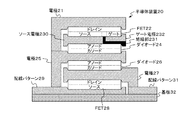
- FIG. 1A and 1B are a cross-sectional view and a plan view illustrating an example of the structure of a semiconductor device according to an embodiment of the present invention. It is a circuit diagram which shows an example of the circuit where the semiconductor device 10 is used. 3 is a conceptual diagram illustrating an example of a wiring pattern 15, a wiring pattern 16, and a wiring pattern 17 provided on a substrate 18. FIG. It is a conceptual diagram for demonstrating an example of the structure of FET14. It is a conceptual diagram for demonstrating an example of the shape of the electrode 13. FIG. 3 is a conceptual diagram for explaining an example of a shape of an electrode 11.
- FIG. 4 is a flowchart showing an example of a manufacturing process of the semiconductor device 10. FIG.
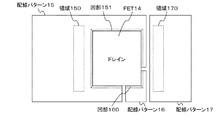
- FIG. 5 is a conceptual diagram for explaining an example of a state in which an FET 14 is disposed on a wiring pattern 15 and a wiring pattern 16.
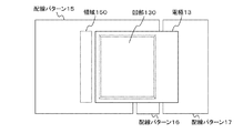
- FIG. 5 is a conceptual diagram for explaining an example of a state in which an electrode 13 is disposed on an FET 14 and a wiring pattern 17.
- 4 is a conceptual diagram for explaining an example of a state in which a diode 12 is disposed on an electrode 13.
- FIG. 6 is a cross-sectional view showing another example of the structure of the semiconductor device 10.
- 2A and 2B are a cross-sectional view and a bottom view showing an example of the structure of the semiconductor module 19.
- FIG. 10 is a cross-sectional view showing another example of the structure of the semiconductor module 19.
- 2A and 2B are a plan view and a cross-sectional view showing an example of protrusions and grooves provided on the wiring pattern 15 and the wiring pattern 16, respectively. It is sectional drawing (a) and top view (b) which show an example of the structure of the semiconductor device 20 which concerns on other embodiment of this invention. It is sectional drawing which shows an example of the structure of the semiconductor device 20 which concerns on other embodiment of this invention.
- 2 is a perspective view illustrating an example of an appearance of a semiconductor device 20.
- FIG. 4 is a conceptual diagram for explaining an example of a shape of an electrode 23.
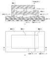
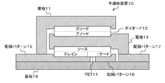
- FIG. 1 is a cross-sectional view (a) and a plan view (b) showing an example of the structure of a semiconductor device 10 according to an embodiment of the present invention.
- FIG. 1A is a cross-sectional view taken along line AA of the semiconductor device 20 of FIG.
- the semiconductor device 10 includes an electrode 11, a diode 12, an electrode 13, a field effect transistor (FET) 14, a wiring pattern 15, a wiring pattern 16, a wiring pattern 17, and a substrate 18.
- the FET 14 is an example of a switching element.
- the semiconductor device 10 shown in this embodiment is used in a circuit as shown in FIG. 2, for example.
- the circuit illustrated in FIG. 2 is a power conversion circuit composed of a three-phase PWM (Pulse Width Modulation) inverter, and is connected between a P power supply line that is a high-voltage DC power supply line and an N power supply line that is a low-voltage DC power supply line. It has a U-phase output unit, a V-phase output unit, and a W-phase output unit.
- PWM Pulse Width Modulation
- the U-phase output unit, V-phase output unit, and W-phase output unit each have two sets of semiconductor devices 10 each having a switching element (FET) and a diode connected in parallel.
- FET switching element
- each FET is ON / OFF controlled by the control circuit, and the direct current supplied from the P power supply line and the N power supply line is converted into an alternating current and supplied to the motor to drive the motor.
- a wiring pattern 15, a wiring pattern 16, and a wiring pattern 17 are formed on the substrate 18 using, for example, Cu (copper).
- the substrate 18 is preferably formed of ceramics such as aluminum nitride having high thermal conductivity and insulation.
- the substrate 18 may be formed of a metal having high thermal conductivity, such as copper or aluminum.
- an insulating layer is formed on the substrate 18 with aluminum nitride or the like, and the wiring patterns 15 to 17 is provided.
- the wiring pattern 15 and the wiring pattern 16 are provided with a concave portion 151 and a concave portion 160, respectively, along the region where the FET 14 is disposed, for example, as shown in FIG.
- the recess 151 is formed thinner than other regions of the wiring pattern 15, and the recess 160 is formed thinner than other regions of the wiring pattern 16.
- the concave portion 151 and the concave portion 160 By providing the concave portion 151 and the concave portion 160, it is possible to improve the positioning accuracy when the FET 14 is placed on the wiring pattern 15 and the wiring pattern 16, and other components are further placed on the FET 14. In this case, it is possible to prevent the FET 14 from shifting on the wiring pattern 15 or the wiring pattern 16.
- the recess 151 and the recess 160 are provided, when the FET 14 is placed after applying a conductive adhesive such as silver nano paste on the wiring pattern 15 and the wiring pattern 16, the conductive adhesive Can be prevented from leaking out to other regions on the wiring pattern 15 or the wiring pattern 16.
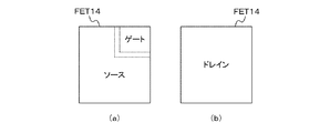
- the FET 14 is formed in a plate shape, for example, and as shown in FIG. 4, a gate and a source are provided on one surface, and a drain is provided on the other surface.
- the FET 14 preferably uses SiC (silicon carbide) as a material.
- the source of the FET 14 is fixed to the recess 151 of the wiring pattern 15 and the gate of the FET 14 is fixed to the recess 160 of the wiring pattern 16 by the conductive bonding agent.
- the conductive bonding agent metal nano paste (for example, silver nano paste) or solder paste can be used.
- the electrode 13 is formed of, for example, Cu or the like in the shape shown in FIG.
- a recess 130 as shown in FIG. 5A is formed on the surface of the electrode 13 connected to the diode 12, and a recess 131 as shown in FIG. 5B is formed on the surface connected to the FET 14. Is done.
- the recess 131 is fixed to the drain of the FET 14 and the leg 132 is fixed to the region 170 of the wiring pattern 17 by a conductive bonding agent such as silver nanopaste.
- the recess 131 is fixed to the FET 14 on the surface (more preferably, the entire surface) where the drain of the FET 14 is provided.
- the diode 12 is formed in a plate shape, for example, and an anode is provided on one surface and a cathode is provided on the other surface.
- the diode 12 preferably uses SiC (silicon carbide) as a material.
- the cathode of the diode 12 is fixed to the recess 130 of the electrode 13 by a conductive bonding agent such as silver nanopaste.
- the diode 12 is fixed to the recess 130 on the surface (more preferably, the entire surface) on which the cathode of the diode 12 is provided.
- the positioning accuracy between the electrode 13 and the FET 14 and the positioning accuracy between the electrode 13 and the diode 12 can be improved, and the conductive bonding agent is used as the electrode. Leakage to other areas on 13 can be prevented.
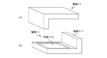
- the electrode 11 is formed of, for example, Cu or the like in the shape shown in FIG.
- a recess 110 as shown in FIG. 6B is formed on the surface of the electrode 11 connected to the diode 12.
- the recess 110 is fixed to the surface of the diode 12 where the anode is provided, and the leg 111 is fixed to the region 150 of the wiring pattern 15.
- the leg 111 is preferably fixed to the diode 12 on the surface (more preferably, the entire surface) on which the anode of the diode 12 is provided.
- the positioning accuracy between the electrode 11 and the diode 12 can be improved, and the conductive bonding agent can be prevented from leaking to other regions on the electrode 13. Can do.
- the semiconductor device 10 of this embodiment is configured by stacking the diode 12 and the FET 14 via the electrode 13, the structure of the conventional power module in which the diode 12 and the FET 14 are arranged side by side on the substrate. As a result, the mounting area can be reduced and the size can be reduced.
- the wiring can be shortened as compared with the case where the diode 12 and the FET 14 are arranged side by side on the substrate. Therefore, loss due to heat of the wiring resistance can be reduced, and power efficiency is improved. Reduction of generated heat can be realized.
- the diode 12 and the FET 14 in the present embodiment may be made using SiC (silicon carbide). In that case, the diode 12 and the FET 14 are at a higher temperature (for example, 300 ° C.) than when made using ordinary silicon. Operation) is possible.
- SiC silicon carbide
- the diode or FET is made using silicon, normal operation can be performed only in a temperature range up to about 150 ° C. Therefore, if a circuit is configured using these diode 12 and FET 14, A cooling device for making the temperature rise less than 150 ° C. must be provided, which may increase the size and complexity of the device.
- the semiconductor device 10 of the present embodiment since SiC (silicon carbide) is used for the diode 12 and the FET 14, operation at a high temperature is possible, a large cooling device is not required, and the device is reduced in size and simplified. Can be realized.
- SiC silicon carbide
- the operating temperature range is up to about 150 ° C., so that the diodes and FETs can be wired by wire bonding.
- SiC silicon carbide
- the diode 12 and the FET 14 can be operated at a temperature of about 300 ° C.
- the wire may melt.
- the diode 12 and the FET 14 are connected not by wires but by a wide electrode or wiring pattern, so that the diode 12 or the FET 14 reaches about 300 ° C. during operation. Even if it exists, a connection state can be maintained without disconnection.
- the diode 12 and the FET 14 are connected not by wires but by wide electrodes and wiring patterns, so that the resistance is low. Wiring becomes possible.
- the FET 14 is used as an example of the switching element.
- a bipolar transistor such as an IGBT (Insulated Gate Bipolar Transistor) may be used instead of the FET 14.
- IGBT Insulated Gate Bipolar Transistor
- FIG. 1 a base is connected to the wiring pattern 16, an emitter is connected to the wiring pattern 15, and a collector is connected to the electrode 13.
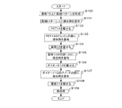
- FIG. 7 is a flowchart showing an example of the manufacturing process of the semiconductor device 10.
- the wiring pattern 15, the wiring pattern 16, and the wiring pattern 17 are formed on the substrate 18 by using, for example, plating or sputtering. For example, it is formed by etching or the like (S100).
- a conductive bonding agent such as a silver nano paste is applied to the wiring pattern 15, the wiring pattern 16, and the wiring pattern 17 (S101). More specifically, a conductive bonding agent such as silver nano paste is applied to the region 150 and the recess 151 of the wiring pattern 15, the recess 160 of the wiring pattern 16, and the region 170 of the wiring pattern 17.
- the FET 14 is placed on the wiring pattern 15 and the wiring pattern 16 coated with the conductive bonding agent (S102). More specifically, the source of the FET 14 is placed on the concave portion 151 of the wiring pattern 15 and the gate of the FET 14 is placed on the concave portion 160 of the wiring pattern 16, resulting in a state as shown in FIG.
- a conductive bonding agent such as silver nano paste is applied to the drain surface of the FET 14 (S103).
- the electrode 13 is placed on the FET 14 and the wiring pattern 17 (S104). More specifically, the concave portion 131 of the electrode 13 is placed on the drain surface of the FET 14 and the leg portion 132 of the electrode 13 is placed on the region 170 of the wiring pattern 17, resulting in a state as shown in FIG.
- a conductive bonding agent such as silver nanopaste is applied to the recess 130 of the electrode 13 (S105).
- the diode 12 is placed on the recess 130 of the electrode 13 (S106). More specifically, the cathode surface of the diode 12 is placed on the concave portion 130 of the electrode 13, for example, as shown in FIG. 10.
- a conductive bonding agent such as silver nano paste is applied to the surface of the anode of the diode 12 (S107).
- the electrode 11 is placed on the diode 12 and the wiring pattern 15 (S108). More specifically, the concave portion 110 of the electrode 11 is placed on the anode surface of the diode 12, and the leg portion 111 of the electrode 11 is placed on the region 150 of the wiring pattern 15, for example, as shown in FIG. It becomes a state.
- the entire semiconductor device 10 is heat-treated, and the conductive bonding agent such as silver nanopaste is solidified (S109), and the manufacturing process of the semiconductor device 10 shown in this flowchart is completed.
- the semiconductor device 10 of the present embodiment it is possible to further reduce the size of the semiconductor device having the switching element and the diode.
- the semiconductor device 10 may be configured as shown in FIG. 11, for example, by providing the source and drain of the FET 14 on the opposite surfaces and attaching the diode 12 on the opposite side.
- the semiconductor device 10 is provided with an insulating layer 192 such as a highly insulating resin on the electrode 11, a heat radiating plate 191 is provided on the insulating layer 192, and the whole is sealed with a mold resin 190.
- the semiconductor module 19 may be configured.
- 12B is a bottom view of the semiconductor module 19, and FIG. 12A is a cross-sectional view taken along the line BB of FIG. 12B.
- the surface of the heat radiating plate 191 opposite to the surface in contact with the insulating layer 192 is exposed to the outside of the semiconductor module 19. Therefore, the heat of the semiconductor module 19 can be released to the outside more efficiently by bringing the heat radiating plate 191 into contact with the metal housing or the like of the device to which the semiconductor module 19 is attached. Further, by providing unevenness and fins on the surface of the heat radiating plate 191 opposite to the surface in contact with the insulating layer 192 to increase the surface area, the heat of the semiconductor module 19 can be released more efficiently to the outside.
- a plurality of through holes 180 are provided in the substrate 18, and solder balls 181 for connecting to the respective through holes 180 on the surface opposite to the surface of the substrate 18 on which the wiring pattern is provided. Is provided.
- a solder ball 181 of a through hole 180 connected to the wiring pattern 15 is disposed in the region 182
- a solder ball 181 of a through hole 180 connected to the wiring pattern 16 is disposed in the region 183
- a wiring is disposed in the region 184.
- Solder balls 181 of the through holes 180 connected to the pattern 17 are arranged. With such a configuration, the semiconductor module 19 can be easily surface-mounted on another circuit board.
- the semiconductor device 10 is provided with a heat radiating plate 191 on the electrode 11 via an insulating layer 192, and the whole is sealed with a mold resin 190 and connected to a wiring pattern on the substrate 18.
- You may comprise as the semiconductor module 19 which provided the lead 40 and the lead 41.
- FIG. 13 a lead connected to the wiring pattern 16 of the gate of the FET 14 is also provided.
- the electrode 11, the electrode 13, the wiring pattern 15, and the wiring pattern 16 are provided with recesses, thereby improving the positioning accuracy of the diode 12 and the FET 14 and preventing positional deviation in the manufacturing process.
- leakage to other regions of the conductive bonding agent such as silver nanopaste can be blocked, the present invention is not limited to this.
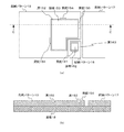
- FIG. 14A is a plan view of the wiring pattern 15, the wiring pattern 16, and the wiring pattern 17, and FIG. 14B is a cross-sectional view taken along the line CC of FIG. 14A.
- a groove 152 is provided along a region 153 where the source of the FET 14 is disposed in the wiring pattern 15, and a protrusion 161 is formed along the region 162 where the gate of the FET 14 is disposed in the wiring pattern 16. Is provided.
- the groove does not need to completely surround the region 153 where the source of the FET 14 is disposed and the region 162 where the gate of the FET 14 is disposed, and the leakage of the conductive adhesive such as a short distance from other signal lines. You may make it provide a groove
- protrusions 154 to 156 are provided along the region 153 where the source of the FET 14 is disposed, and in the wiring pattern 16, the region along the region 162 where the gate of the FET 14 is disposed.
- the protrusion 161 may be provided.
- the protrusions 154 to 156 in FIG. 14 exemplify those having a length in the direction along the region 153 longer than the height from the wiring pattern 15, but the length in the direction along the region 153 than the height from the wiring pattern 15. May be the same or shorter.
- the electrodes 11 and 13 may be provided with the above-described grooves, protrusions, or both instead of the recesses.
- the semiconductor device 10 in which the FET 14 and the diode 12 are stacked one by one is illustrated.
- the present invention is not limited to this, and the semiconductor device 10 is stacked by stacking two or more FETs and diodes. It may be configured.
- 15 to 17 are conceptual diagrams showing an example of the structure of the semiconductor device 20 when two FETs and two diodes are stacked.
- 15B is a plan view of the semiconductor device 20
- FIG. 15A is a DD cross-sectional view of the semiconductor device 20 of FIG. 15B
- FIG. 16 is FIG. 15B.
- FIG. 6 is an EE cross-sectional view of the semiconductor device 20 of FIG.
- the semiconductor device 20 includes an electrode 21, an FET 22, an electrode 23, a diode 24, an electrode 25, a diode 26, an electrode 27, an FET 28, a wiring pattern 29, a wiring pattern 30, a wiring pattern 31, a substrate 32, a wiring pattern 33, and a wiring pattern 34. Is provided.
- a wiring pattern 29, a wiring pattern 30, a wiring pattern 31, a wiring pattern 33, and a wiring pattern are formed on the substrate 32 formed using ceramics such as aluminum nitride having high thermal conductivity and high insulation, for example, using Cu or the like. 34 is formed.
- the FET 28 is formed in, for example, a plate shape, and the source of the FET 28 is fixed to the concave portion of the wiring pattern 29 and the gate of the FET 28 is fixed to the concave portion of the wiring pattern 30 by a conductive bonding agent such as silver nanopaste.
- the electrode 27 is formed, for example, with Cu or the like in the shape shown in FIG. 5, and one recess is fixed to the drain of the FET 28 with a conductive bonding agent such as silver nanopaste, and the other recess is the cathode of the diode 26.
- the leg portion is fixed to the wiring pattern 31.
- the diode 26 is formed in, for example, a plate shape, and the cathode provided on one surface is in the concave portion of the electrode 27, the anode provided on the other surface is in the concave portion of the electrode 25, and a conductive bonding agent such as silver nano paste. It is fixed by.
- the electrode 25 is formed, for example, with Cu or the like in the shape shown in FIG. 5, and one recess is fixed to the anode of the diode 26 and the other recess is the diode 24 with a conductive bonding agent such as silver nanopaste.
- the leg is fixed to the wiring pattern 29 and fixed to the cathode.
- the diode 24 is formed in, for example, a plate shape, and a cathode provided on one surface is in the recess of the electrode 25, an anode provided on the other surface is in the recess of the electrode 23, and a conductive bonding agent such as silver nano paste. It is fixed by.
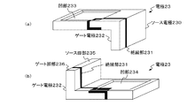
- the electrode 23 is formed of, for example, Cu or the like in the shape shown in FIG.
- the electrode 23 includes a source electrode 230, an insulating portion 231, and a gate electrode 232.
- a recess 233 as shown in FIG. 18A is formed on the surface of the electrode 23 connected to the FET 22, and a recess 234 as shown in FIG. 18B is formed on the surface connected to the diode 24. Is done.
- the source electrode 230 is connected to the anode of the diode 24 at the surface of the recess 234 and is connected to the source of the FET 22 at a part of the surface of the recess 233.
- the gate electrode 232 is connected to the gate of the FET 22 on a part of the surface of the recess 233.
- the insulating part 231 insulates the source electrode 230 and the insulating part 231.
- the source electrode 230 of the electrode 23 is connected to the wiring pattern 33 at the source leg 235, and the gate electrode 232 is connected to the wiring pattern 34 at the gate leg 236 (see FIG. 17B).
- the FET 22 is formed in a plate shape, for example, and the source of the FET 22 is fixed to the insulating portion 231 of the electrode 23 and the gate of the FET 22 is fixed to the gate electrode 232 by a conductive bonding agent such as silver nanopaste.
- the electrode 21 is formed in, for example, the shape shown in FIG. 6 with Cu or the like, for example, and the recess is fixed to the drain of the FET 22 and the leg is fixed to the electrode 25 with a conductive bonding agent such as silver nanopaste.
- each phase output unit having two semiconductor devices 10 can be configured by one semiconductor device 20. Thereby, further miniaturization of the circuit shown in FIG. 2 can be realized.
Landscapes
- Metal-Oxide And Bipolar Metal-Oxide Semiconductor Integrated Circuits (AREA)
- Junction Field-Effect Transistors (AREA)
- Physics & Mathematics (AREA)
- Geometry (AREA)
Abstract
Description
Claims (9)
- 半導体装置であって、
基板上に設けられたFET(Field effect transistor)と、
前記FETを挟んで前記基板と反対側に設けられた第1の電極と、
前記第1の電極を挟んで前記FETと反対側に設けられたダイオードと、
前記ダイオードを挟んで前記第1の電極と反対側に設けられた第2の電極と、
を備え、
前記FETは、板状に形成されており、
一方の面にソースおよびゲートが設けられ、他方の面にドレインが設けられ、
前記ソースが前記基板上の第1の配線パターンに接続され、
前記ゲートが前記基板上の第2の配線パターンに接続され、
前記ドレインが前記第1の電極に接続され、
前記第1の電極の脚部と、前記基板上の前記第1の配線パターン及び前記第2の配線パターンとは異なる配線パターンとが接続され、
前記ダイオードは、板状に形成されており、
一方の面にアノードが設けられ、他方の面にカソードが設けられ、
前記カソードが前記第1の電極に接続され、
前記アノードが前記第2の電極に接続され、
前記第2の電極の脚部と、前記第1の配線パターンとが接続され、
前記第1の電極の脚部と、前記第2の電極の脚部とは、前記FETを挟んで対向している
ことを特徴とする半導体装置。 - 半導体装置であって、
基板上に設けられたFET(Field effect transistor)と、
前記FETを挟んで前記基板と反対側に設けられた第1の電極と、
前記第1の電極を挟んで前記FETと反対側に設けられたダイオードと、
前記ダイオードを挟んで前記第1の電極と反対側に設けられた第2の電極と、
を備え、
前記FETは、板状に形成されており、
一方の面にソースおよびゲートが設けられ、他方の面にドレインが設けられ、
前記ソースが前記基板上の第1の配線パターンに接続され、
前記ゲートが前記基板上の第2の配線パターンに接続され、
前記ドレインが前記第1の電極に接続され、
前記ダイオードは、板状に形成されており、
一方の面にアノードが設けられ、他方の面にカソードが設けられ、
前記カソードが前記第1の電極に接続され、
前記アノードが前記第2の電極に接続され、
前記第2の電極と前記第1の配線パターンとが接続され、
前記第1の電極の前記ダイオードと接続する面は、前記FET及び前記ダイオードより大きく、
前記FETの辺と平行かつ前記ソース及び前記ゲートを通る線を含み、前記FETの前記一方の面に直交する面で前記半導体装置を切断した断面において、前記カソードの長さは、前記ソースの長さと前記ゲートの長さの和よりも長い
ことを特徴とする半導体装置。 - 請求項1又は2に記載の半導体装置であって、
前記FETの辺と平行かつ前記ソース及び前記ゲートを通る線を含み、前記FETの前記一方の面に直交する面で前記半導体装置を切断した断面において、前記第1の電極及び前記第2の電極はL字形状であり、
前記第1の電極及び前記第2の電極は、前記L字形状のうちの長辺に相当する部分が前記基板と平行、かつ前記L字形状のうちの短辺に相当する部分の先端が前記基板上のパターンと当接するように設けられる
ことを特徴とする半導体装置。 - 請求項1から3のいずれかに記載の半導体装置であって、
前記第1および第2の電極は、少なくとも一部が板状の電極であり、
前記第1の電極は、
前記FETにおける前記ドレインの面で前記FETと接続し、前記ダイオードにおける前記カソードの面で前記ダイオードと接続し、
前記第2の電極は、
前記ダイオードにおける前記アノードの面で前記ダイオードと接続し、
前記第1の配線パターンは、
前記FETにおける前記ソースの面で前記FETと接続していることを特徴とする半導体装置。 - 請求項1から4のいずれかに記載の半導体装置であって、
前記第1の電極には、
前記FETと接続される面に、前記第1の電極と前記FETとの位置を合わせるための窪みまたは突起が設けられ、
前記ダイオードと接続される面に、前記第1の電極と前記ダイオードとの位置を合わせるための窪みまたは突起が設けられており、
前記第2の電極には、
前記ダイオードと接続される面に、前記第2の電極と前記ダイオードとの位置を合わせるための窪みまたは突起が設けられており、
前記1の配線パターンには、
前記FETと接続される面に、前記第1の配線パターンと前記FETとの位置を合わせるための窪みまたは突起が設けられていることを特徴とする半導体装置。 - 請求項1から5のいずれか一項に記載の半導体装置であって、
前記第1の電極と前記FET、前記第1の電極と前記ダイオード、前記第2の電極と前記ダイオード、前記第1の配線パターンと前記FETは、それぞれ導電性の接合剤で接続され、
前記第1の電極における前記FETが接続される側および前記ダイオードが接続される側、前記第2の電極における前記ダイオードが接続される側、ならびに、前記第1の配線パターンにおける前記FETが接続される側には、それぞれ、前記導電性の接合剤の広がりを抑えるための堰き止め部が設けられていることを特徴とする半導体装置。 - 請求項1から6のいずれか一項に記載の半導体装置において、
前記第2の電極を挟んで前記ダイオードと反対側に設けられ絶縁層と、
前記絶縁層を挟んで前記第2の電極と反対側に設けられた放熱板と
をさらに備え、
前記半導体装置を樹脂封止し、前記放熱板において前記絶縁層に接する面と反対側の部分を外部に露出させたことを特徴とする半導体装置。 - 半導体装置であって、
基板上に設けられた第1のFET(Field effect transistor)と、
前記第1のFETを挟んで前記基板と反対側に設けられた第1の電極と、
前記第1の電極を挟んで前記第1のFETと反対側に設けられた第1のダイオードと、
前記第1のダイオードを挟んで前記第1の電極と反対側に設けられた第2の電極と、
前記第2の電極を挟んで前記第1のダイオードと反対側に設けられた第2のダイオードと、
前記第2のダイオードを挟んで前記第2の電極と反対側に設けられた第3の電極と、
前記第3の電極を挟んで前記第2のダイオードと反対側に設けられた第2のFETと、
前記第2のFETを挟んで前記第3の電極と反対側に設けられた第4の電極と
を備え、
前記第1および第2のFETは、それぞれ板状に形成されており、一方の面にソースおよびゲートが設けられ、他方の面にドレインが設けられ、
前記第1のFETのソースが前記基板上に設けられた第1の配線パターンに接続され、
前記第1のFETのゲートが前記基板上に設けられた第2の配線パターンに接続され、
前記第1のFETのドレインが前記第1の電極に接続され、
前記第1の電極の脚部と、前記基板上の前記第1の配線パターン及び前記第2の配線パターンとは異なる配線パターンとが接続され、
前記第2のFETのソースが前記第3の電極に接続され、
前記第2のFETのゲートが第5の電極に接続され、
前記第2のFETのドレインが前記第4の電極に接続され、
前記第1および第2のダイオードは、それぞれ、少なくとも一部が板状に形成されており、一方の面にアノードが設けられ、他方の面にカソードが設けられ、
前記第1のダイオードのカソードが前記第1の電極に接続され、
前記第1のダイオードのアノードが前記第2の電極に接続され、
前記第2のダイオードのカソードが前記第2の電極に接続され、
前記第2のダイオードのアノードが前記第3の電極に接続され、
前記第2の電極の脚部と前記第1の配線パターンとが接続され、
前記第1の電極の脚部と、前記第2の電極の脚部及び前記第4の電極の脚部とは、前記第1のFET、前記第2のFET、前記第1のダイオード及び前記第2のダイオードを挟んで対向している
ことを特徴とする半導体装置。 - 半導体装置であって、
基板上に設けられた第1のFET(Field effect transistor)と、
前記第1のFETを挟んで前記基板と反対側に設けられた第1の電極と、
前記第1の電極を挟んで前記第1のFETと反対側に設けられた第1のダイオードと、
前記第1のダイオードを挟んで前記第1の電極と反対側に設けられた第2の電極と、
前記第2の電極を挟んで前記第1のダイオードと反対側に設けられた第2のダイオードと、
前記第2のダイオードを挟んで前記第2の電極と反対側に設けられた第3の電極と、
前記第3の電極を挟んで前記第2のダイオードと反対側に設けられた第2のFETと、
前記第2のFETを挟んで前記第3の電極と反対側に設けられた第4の電極と
を備え、
前記第1および第2のFETは、それぞれ板状に形成されており、一方の面にソースおよびゲートが設けられ、他方の面にドレインが設けられ、
前記第1のFETのソースが前記基板上に設けられた第1の配線パターンに接続され、
前記第1のFETのゲートが前記基板上に設けられた第2の配線パターンに接続され、
前記第1のFETのドレインが前記第1の電極に接続され、
前記第2のFETのソースが前記第3の電極に接続され、
前記第2のFETのゲートが第5の電極に接続され、
前記第2のFETのドレインが前記第4の電極に接続され、
前記第1および第2のダイオードは、それぞれ、少なくとも一部が板状に形成されており、一方の面にアノードが設けられ、他方の面にカソードが設けられ、
前記第1のダイオードのカソードが前記第1の電極に接続され、
前記第1のダイオードのアノードが前記第2の電極に接続され、
前記第2のダイオードのカソードが前記第2の電極に接続され、
前記第2のダイオードのアノードが前記第3の電極に接続され、
前記第2の電極と前記第4の電極と前記第1の配線パターンとが接続され、
前記第1の電極の前記第1のダイオードと接続する面は、前記第1のFET及び前記第1のダイオードより大きく、
前記第1のFETの辺と平行かつ前記第1のFETのソース及び前記第1のFETのゲートを通る線を含み、前記第1のFETの前記一方の面に直交する面で前記半導体装置を切断した断面において、前記第1のダイオードのカソードの長さは、前記第1のFETのソースの長さと前記第1のFETのゲートの長さの和よりも長い
ことを特徴とする半導体装置。
Priority Applications (4)
| Application Number | Priority Date | Filing Date | Title |
|---|---|---|---|
| KR1020147002501A KR20150056496A (ko) | 2012-09-19 | 2013-08-30 | 반도체 장치 |
| US14/236,228 US9159715B2 (en) | 2012-09-19 | 2013-08-30 | Miniaturized semiconductor device |
| EP13823908.2A EP2899756A4 (en) | 2012-09-19 | 2013-08-30 | SEMICONDUCTOR COMPONENT |
| CN201380002517.8A CN103828044A (zh) | 2012-09-19 | 2013-08-30 | 半导体器件 |
Applications Claiming Priority (2)
| Application Number | Priority Date | Filing Date | Title |
|---|---|---|---|
| JP2012-205618 | 2012-09-19 | ||
| JP2012205618A JP5357315B1 (ja) | 2012-09-19 | 2012-09-19 | 半導体装置 |
Publications (1)
| Publication Number | Publication Date |
|---|---|
| WO2014045842A1 true WO2014045842A1 (ja) | 2014-03-27 |
Family
ID=49850243
Family Applications (1)
| Application Number | Title | Priority Date | Filing Date |
|---|---|---|---|
| PCT/JP2013/073335 Ceased WO2014045842A1 (ja) | 2012-09-19 | 2013-08-30 | 半導体装置 |
Country Status (6)
| Country | Link |
|---|---|
| US (1) | US9159715B2 (ja) |
| EP (1) | EP2899756A4 (ja) |
| JP (1) | JP5357315B1 (ja) |
| KR (1) | KR20150056496A (ja) |
| CN (1) | CN103828044A (ja) |
| WO (1) | WO2014045842A1 (ja) |
Cited By (1)
| Publication number | Priority date | Publication date | Assignee | Title |
|---|---|---|---|---|
| WO2016024333A1 (ja) * | 2014-08-12 | 2016-02-18 | 新電元工業株式会社 | 半導体モジュール |
Families Citing this family (10)
| Publication number | Priority date | Publication date | Assignee | Title |
|---|---|---|---|---|
| CN105720030B (zh) * | 2014-12-04 | 2018-07-31 | 万国半导体股份有限公司 | 基于小型栅极金属片的封装方法及封装结构及金属片框架 |
| US9922970B2 (en) * | 2015-02-13 | 2018-03-20 | Qualcomm Incorporated | Interposer having stacked devices |
| KR102563860B1 (ko) * | 2015-12-02 | 2023-08-03 | 마이크로 모듈 테크놀로지 가부시키가이샤 | 광학 장치 및 광학 장치의 제조 방법 |
| US11276663B2 (en) * | 2017-05-19 | 2022-03-15 | Shindengen Electric Manufacturing Co., Ltd. | Electronic module |
| JP6997552B2 (ja) * | 2017-07-28 | 2022-01-17 | 日立Astemo株式会社 | 電力変換装置及び電力変換装置の製造方法 |
| WO2019082333A1 (ja) * | 2017-10-26 | 2019-05-02 | 新電元工業株式会社 | 電子部品 |
| JP7204174B2 (ja) * | 2018-07-19 | 2023-01-16 | マイクロモジュールテクノロジー株式会社 | 半導体装置及び半導体装置の製造方法 |
| US11037917B1 (en) * | 2019-12-11 | 2021-06-15 | Littelfuse, Inc. | Semiconductor device module and method of assembly |
| CN111244074B (zh) * | 2020-03-10 | 2025-07-11 | 英诺赛科(苏州)半导体有限公司 | 氮化镓半导体器件及其封装方法 |
| US20240282668A1 (en) * | 2023-02-22 | 2024-08-22 | Semiconductor Components Industries, Llc | Protection dam for a power module with spacers |
Citations (4)
| Publication number | Priority date | Publication date | Assignee | Title |
|---|---|---|---|---|
| JP2005302951A (ja) * | 2004-04-09 | 2005-10-27 | Toshiba Corp | 電力用半導体装置パッケージ |
| JP2006134990A (ja) * | 2004-11-04 | 2006-05-25 | Fuji Electric Holdings Co Ltd | 半導体装置 |
| WO2009020061A1 (ja) * | 2007-08-07 | 2009-02-12 | Rohm Co., Ltd. | 高効率モジュール |
| JP2009295794A (ja) * | 2008-06-05 | 2009-12-17 | Mitsubishi Electric Corp | 樹脂封止型半導体装置とその製造方法 |
Family Cites Families (4)
| Publication number | Priority date | Publication date | Assignee | Title |
|---|---|---|---|---|
| US7554188B2 (en) * | 2006-04-13 | 2009-06-30 | International Rectifier Corporation | Low inductance bond-wireless co-package for high power density devices, especially for IGBTs and diodes |
| JP2009105389A (ja) | 2007-10-02 | 2009-05-14 | Rohm Co Ltd | パワーモジュール |
| JP5691475B2 (ja) * | 2010-12-15 | 2015-04-01 | 富士電機株式会社 | 半導体装置およびその製造方法 |
| US8431979B2 (en) * | 2011-04-01 | 2013-04-30 | Texas Instruments Incorporated | Power converter having integrated capacitor |
-
2012
- 2012-09-19 JP JP2012205618A patent/JP5357315B1/ja active Active
-
2013
- 2013-08-30 KR KR1020147002501A patent/KR20150056496A/ko not_active Withdrawn
- 2013-08-30 WO PCT/JP2013/073335 patent/WO2014045842A1/ja not_active Ceased
- 2013-08-30 US US14/236,228 patent/US9159715B2/en active Active
- 2013-08-30 CN CN201380002517.8A patent/CN103828044A/zh active Pending
- 2013-08-30 EP EP13823908.2A patent/EP2899756A4/en not_active Withdrawn
Patent Citations (4)
| Publication number | Priority date | Publication date | Assignee | Title |
|---|---|---|---|---|
| JP2005302951A (ja) * | 2004-04-09 | 2005-10-27 | Toshiba Corp | 電力用半導体装置パッケージ |
| JP2006134990A (ja) * | 2004-11-04 | 2006-05-25 | Fuji Electric Holdings Co Ltd | 半導体装置 |
| WO2009020061A1 (ja) * | 2007-08-07 | 2009-02-12 | Rohm Co., Ltd. | 高効率モジュール |
| JP2009295794A (ja) * | 2008-06-05 | 2009-12-17 | Mitsubishi Electric Corp | 樹脂封止型半導体装置とその製造方法 |
Non-Patent Citations (1)
| Title |
|---|
| See also references of EP2899756A4 * |
Cited By (2)
| Publication number | Priority date | Publication date | Assignee | Title |
|---|---|---|---|---|
| WO2016024333A1 (ja) * | 2014-08-12 | 2016-02-18 | 新電元工業株式会社 | 半導体モジュール |
| JP5930565B1 (ja) * | 2014-08-12 | 2016-06-08 | 新電元工業株式会社 | 半導体モジュール |
Also Published As
| Publication number | Publication date |
|---|---|
| EP2899756A4 (en) | 2016-11-02 |
| JP5357315B1 (ja) | 2013-12-04 |
| JP2014060325A (ja) | 2014-04-03 |
| US20150206864A1 (en) | 2015-07-23 |
| US9159715B2 (en) | 2015-10-13 |
| EP2899756A1 (en) | 2015-07-29 |
| CN103828044A (zh) | 2014-05-28 |
| KR20150056496A (ko) | 2015-05-26 |
Similar Documents
| Publication | Publication Date | Title |
|---|---|---|
| JP5357315B1 (ja) | 半導体装置 | |
| EP3107120B1 (en) | Power semiconductor module | |
| JP5841500B2 (ja) | スタック型ハーフブリッジ電力モジュール | |
| JP6520437B2 (ja) | 半導体装置 | |
| EP2814059B1 (en) | Semiconductor device | |
| EP3104412B1 (en) | Power semiconductor module | |
| WO2013021647A1 (ja) | 半導体モジュール、半導体モジュールを備えた半導体装置、および半導体モジュールの製造方法 | |
| US10720383B2 (en) | Semiconductor device configuring upper and lower arms including auxiliary terminals | |
| TWI716075B (zh) | 功率模組 | |
| JP7163828B2 (ja) | 半導体モジュールとそれを備えた半導体装置 | |
| JP6490027B2 (ja) | 半導体装置 | |
| WO2022059251A1 (ja) | 半導体装置 | |
| JPWO2013171946A1 (ja) | 半導体装置の製造方法および半導体装置 | |
| JP6480856B2 (ja) | 半導体モジュール | |
| WO2016203743A1 (ja) | 半導体装置 | |
| WO2014192093A1 (ja) | 半導体装置 | |
| JPWO2013047231A1 (ja) | 半導体装置及びその製造方法 | |
| JP2017054842A (ja) | 配線基板、半導体装置、及び半導体パッケージ | |
| KR101776425B1 (ko) | 파워 모듈 | |
| CN105529309A (zh) | 半导体装置 | |
| JP2017054855A (ja) | 半導体装置、及び半導体パッケージ | |
| WO2018047485A1 (ja) | パワーモジュールおよびインバータ装置 | |
| JP7012453B2 (ja) | ブリッジレッグ回路組立品およびフルブリッジ回路組立品 | |
| WO2013105456A1 (ja) | 回路基板および電子デバイス | |
| US20160351469A1 (en) | Semiconductor device |
Legal Events
| Date | Code | Title | Description |
|---|---|---|---|
| ENP | Entry into the national phase |
Ref document number: 20147002501 Country of ref document: KR Kind code of ref document: A |
|
| WWE | Wipo information: entry into national phase |
Ref document number: 14236228 Country of ref document: US |
|
| REEP | Request for entry into the european phase |
Ref document number: 2013823908 Country of ref document: EP |
|
| WWE | Wipo information: entry into national phase |
Ref document number: 2013823908 Country of ref document: EP |
|
| 121 | Ep: the epo has been informed by wipo that ep was designated in this application |
Ref document number: 13823908 Country of ref document: EP Kind code of ref document: A1 |
|
| NENP | Non-entry into the national phase |
Ref country code: DE |