WO2014046093A1 - 異方性導電接着剤 - Google Patents
異方性導電接着剤 Download PDFInfo
- Publication number
- WO2014046093A1 WO2014046093A1 PCT/JP2013/075048 JP2013075048W WO2014046093A1 WO 2014046093 A1 WO2014046093 A1 WO 2014046093A1 JP 2013075048 W JP2013075048 W JP 2013075048W WO 2014046093 A1 WO2014046093 A1 WO 2014046093A1
- Authority
- WO
- WIPO (PCT)
- Prior art keywords
- particles
- anisotropic conductive
- conductive adhesive
- solder
- led
- Prior art date
- Legal status (The legal status is an assumption and is not a legal conclusion. Google has not performed a legal analysis and makes no representation as to the accuracy of the status listed.)
- Ceased
Links
Images



Classifications
-
- B—PERFORMING OPERATIONS; TRANSPORTING
- B23—MACHINE TOOLS; METAL-WORKING NOT OTHERWISE PROVIDED FOR
- B23K—SOLDERING OR UNSOLDERING; WELDING; CLADDING OR PLATING BY SOLDERING OR WELDING; CUTTING BY APPLYING HEAT LOCALLY, e.g. FLAME CUTTING; WORKING BY LASER BEAM
- B23K35/00—Rods, electrodes, materials, or media, for use in soldering, welding, or cutting
- B23K35/22—Rods, electrodes, materials, or media, for use in soldering, welding, or cutting characterised by the composition or nature of the material
- B23K35/36—Selection of non-metallic compositions, e.g. coatings or fluxes; Selection of soldering or welding materials, conjoint with selection of non-metallic compositions, both selections being of interest
-
- B—PERFORMING OPERATIONS; TRANSPORTING
- B23—MACHINE TOOLS; METAL-WORKING NOT OTHERWISE PROVIDED FOR
- B23K—SOLDERING OR UNSOLDERING; WELDING; CLADDING OR PLATING BY SOLDERING OR WELDING; CUTTING BY APPLYING HEAT LOCALLY, e.g. FLAME CUTTING; WORKING BY LASER BEAM
- B23K1/00—Soldering, e.g. brazing, or unsoldering
- B23K1/0008—Soldering, e.g. brazing, or unsoldering specially adapted for particular articles or work
- B23K1/0016—Soldering of electronic components
-
- B—PERFORMING OPERATIONS; TRANSPORTING
- B23—MACHINE TOOLS; METAL-WORKING NOT OTHERWISE PROVIDED FOR
- B23K—SOLDERING OR UNSOLDERING; WELDING; CLADDING OR PLATING BY SOLDERING OR WELDING; CUTTING BY APPLYING HEAT LOCALLY, e.g. FLAME CUTTING; WORKING BY LASER BEAM
- B23K35/00—Rods, electrodes, materials, or media, for use in soldering, welding, or cutting
- B23K35/02—Rods, electrodes, materials, or media, for use in soldering, welding, or cutting characterised by mechanical features, e.g. shape
- B23K35/0222—Rods, electrodes, materials, or media, for use in soldering, welding, or cutting characterised by mechanical features, e.g. shape for use in soldering or brazing
- B23K35/0244—Powders, particles or spheres; Preforms made therefrom
- B23K35/025—Pastes, creams or slurries
-
- B—PERFORMING OPERATIONS; TRANSPORTING
- B23—MACHINE TOOLS; METAL-WORKING NOT OTHERWISE PROVIDED FOR
- B23K—SOLDERING OR UNSOLDERING; WELDING; CLADDING OR PLATING BY SOLDERING OR WELDING; CUTTING BY APPLYING HEAT LOCALLY, e.g. FLAME CUTTING; WORKING BY LASER BEAM
- B23K35/00—Rods, electrodes, materials, or media, for use in soldering, welding, or cutting
- B23K35/22—Rods, electrodes, materials, or media, for use in soldering, welding, or cutting characterised by the composition or nature of the material
- B23K35/24—Selection of soldering or welding materials proper
-
- C—CHEMISTRY; METALLURGY
- C09—DYES; PAINTS; POLISHES; NATURAL RESINS; ADHESIVES; COMPOSITIONS NOT OTHERWISE PROVIDED FOR; APPLICATIONS OF MATERIALS NOT OTHERWISE PROVIDED FOR
- C09J—ADHESIVES; NON-MECHANICAL ASPECTS OF ADHESIVE PROCESSES IN GENERAL; ADHESIVE PROCESSES NOT PROVIDED FOR ELSEWHERE; USE OF MATERIALS AS ADHESIVES
- C09J11/00—Features of adhesives not provided for in group C09J9/00, e.g. additives
-
- C—CHEMISTRY; METALLURGY
- C09—DYES; PAINTS; POLISHES; NATURAL RESINS; ADHESIVES; COMPOSITIONS NOT OTHERWISE PROVIDED FOR; APPLICATIONS OF MATERIALS NOT OTHERWISE PROVIDED FOR
- C09J—ADHESIVES; NON-MECHANICAL ASPECTS OF ADHESIVE PROCESSES IN GENERAL; ADHESIVE PROCESSES NOT PROVIDED FOR ELSEWHERE; USE OF MATERIALS AS ADHESIVES
- C09J9/00—Adhesives characterised by their physical nature or the effects produced, e.g. glue sticks
- C09J9/02—Electrically-conducting adhesives
-
- H—ELECTRICITY
- H01—ELECTRIC ELEMENTS
- H01B—CABLES; CONDUCTORS; INSULATORS; SELECTION OF MATERIALS FOR THEIR CONDUCTIVE, INSULATING OR DIELECTRIC PROPERTIES
- H01B1/00—Conductors or conductive bodies characterised by the conductive materials; Selection of materials as conductors
- H01B1/20—Conductive material dispersed in non-conductive organic material
- H01B1/22—Conductive material dispersed in non-conductive organic material the conductive material comprising metals or alloys
-
- H—ELECTRICITY
- H05—ELECTRIC TECHNIQUES NOT OTHERWISE PROVIDED FOR
- H05K—PRINTED CIRCUITS; CASINGS OR CONSTRUCTIONAL DETAILS OF ELECTRIC APPARATUS; MANUFACTURE OF ASSEMBLAGES OF ELECTRICAL COMPONENTS
- H05K13/00—Apparatus or processes specially adapted for manufacturing or adjusting assemblages of electric components
- H05K13/04—Mounting of components, e.g. of leadless components
- H05K13/046—Surface mounting
- H05K13/0465—Surface mounting by soldering
-
- H—ELECTRICITY
- H05—ELECTRIC TECHNIQUES NOT OTHERWISE PROVIDED FOR
- H05K—PRINTED CIRCUITS; CASINGS OR CONSTRUCTIONAL DETAILS OF ELECTRIC APPARATUS; MANUFACTURE OF ASSEMBLAGES OF ELECTRICAL COMPONENTS
- H05K3/00—Apparatus or processes for manufacturing printed circuits
- H05K3/30—Assembling printed circuits with electric components, e.g. with resistors
- H05K3/32—Assembling printed circuits with electric components, e.g. with resistors electrically connecting electric components or wires to printed circuits
- H05K3/34—Assembling printed circuits with electric components, e.g. with resistors electrically connecting electric components or wires to printed circuits by soldering
- H05K3/3465—Application of solder
- H05K3/3485—Application of solder paste, slurry or powder
-
- H—ELECTRICITY
- H10—SEMICONDUCTOR DEVICES; ELECTRIC SOLID-STATE DEVICES NOT OTHERWISE PROVIDED FOR
- H10H—INORGANIC LIGHT-EMITTING SEMICONDUCTOR DEVICES HAVING POTENTIAL BARRIERS
- H10H20/00—Individual inorganic light-emitting semiconductor devices having potential barriers, e.g. light-emitting diodes [LED]
- H10H20/80—Constructional details
- H10H20/85—Packages
- H10H20/857—Interconnections, e.g. lead-frames, bond wires or solder balls
-
- H—ELECTRICITY
- H10—SEMICONDUCTOR DEVICES; ELECTRIC SOLID-STATE DEVICES NOT OTHERWISE PROVIDED FOR
- H10W—GENERIC PACKAGES, INTERCONNECTIONS, CONNECTORS OR OTHER CONSTRUCTIONAL DETAILS OF DEVICES COVERED BY CLASS H10
- H10W20/00—Interconnections in chips, wafers or substrates
- H10W20/40—Interconnections external to wafers or substrates, e.g. back-end-of-line [BEOL] metallisations or vias connecting to gate electrodes
- H10W20/41—Interconnections external to wafers or substrates, e.g. back-end-of-line [BEOL] metallisations or vias connecting to gate electrodes characterised by their conductive parts
- H10W20/44—Conductive materials thereof
- H10W20/4473—Conductive organic materials, e.g. conductive adhesives or conductive inks
-
- C—CHEMISTRY; METALLURGY
- C08—ORGANIC MACROMOLECULAR COMPOUNDS; THEIR PREPARATION OR CHEMICAL WORKING-UP; COMPOSITIONS BASED THEREON
- C08K—Use of inorganic or non-macromolecular organic substances as compounding ingredients
- C08K2201/00—Specific properties of additives
- C08K2201/001—Conductive additives
-
- C—CHEMISTRY; METALLURGY
- C08—ORGANIC MACROMOLECULAR COMPOUNDS; THEIR PREPARATION OR CHEMICAL WORKING-UP; COMPOSITIONS BASED THEREON
- C08K—Use of inorganic or non-macromolecular organic substances as compounding ingredients
- C08K9/00—Use of pretreated ingredients
- C08K9/02—Ingredients treated with inorganic substances
-
- H—ELECTRICITY
- H10—SEMICONDUCTOR DEVICES; ELECTRIC SOLID-STATE DEVICES NOT OTHERWISE PROVIDED FOR
- H10W—GENERIC PACKAGES, INTERCONNECTIONS, CONNECTORS OR OTHER CONSTRUCTIONAL DETAILS OF DEVICES COVERED BY CLASS H10
- H10W40/00—Arrangements for thermal protection or thermal control
- H10W40/20—Arrangements for cooling
- H10W40/25—Arrangements for cooling characterised by their materials
- H10W40/251—Organics
-
- H—ELECTRICITY
- H10—SEMICONDUCTOR DEVICES; ELECTRIC SOLID-STATE DEVICES NOT OTHERWISE PROVIDED FOR
- H10W—GENERIC PACKAGES, INTERCONNECTIONS, CONNECTORS OR OTHER CONSTRUCTIONAL DETAILS OF DEVICES COVERED BY CLASS H10
- H10W72/00—Interconnections or connectors in packages
- H10W72/071—Connecting or disconnecting
- H10W72/072—Connecting or disconnecting of bump connectors
-
- H—ELECTRICITY
- H10—SEMICONDUCTOR DEVICES; ELECTRIC SOLID-STATE DEVICES NOT OTHERWISE PROVIDED FOR
- H10W—GENERIC PACKAGES, INTERCONNECTIONS, CONNECTORS OR OTHER CONSTRUCTIONAL DETAILS OF DEVICES COVERED BY CLASS H10
- H10W72/00—Interconnections or connectors in packages
- H10W72/071—Connecting or disconnecting
- H10W72/072—Connecting or disconnecting of bump connectors
- H10W72/07231—Techniques
- H10W72/07236—Soldering or alloying
-
- H—ELECTRICITY
- H10—SEMICONDUCTOR DEVICES; ELECTRIC SOLID-STATE DEVICES NOT OTHERWISE PROVIDED FOR
- H10W—GENERIC PACKAGES, INTERCONNECTIONS, CONNECTORS OR OTHER CONSTRUCTIONAL DETAILS OF DEVICES COVERED BY CLASS H10
- H10W72/00—Interconnections or connectors in packages
- H10W72/071—Connecting or disconnecting
- H10W72/072—Connecting or disconnecting of bump connectors
- H10W72/07251—Connecting or disconnecting of bump connectors characterised by changes in properties of the bump connectors during connecting
- H10W72/07252—Connecting or disconnecting of bump connectors characterised by changes in properties of the bump connectors during connecting changes in structures or sizes
-
- H—ELECTRICITY
- H10—SEMICONDUCTOR DEVICES; ELECTRIC SOLID-STATE DEVICES NOT OTHERWISE PROVIDED FOR
- H10W—GENERIC PACKAGES, INTERCONNECTIONS, CONNECTORS OR OTHER CONSTRUCTIONAL DETAILS OF DEVICES COVERED BY CLASS H10
- H10W72/00—Interconnections or connectors in packages
- H10W72/071—Connecting or disconnecting
- H10W72/072—Connecting or disconnecting of bump connectors
- H10W72/07251—Connecting or disconnecting of bump connectors characterised by changes in properties of the bump connectors during connecting
- H10W72/07253—Connecting or disconnecting of bump connectors characterised by changes in properties of the bump connectors during connecting changes in shapes
-
- H—ELECTRICITY
- H10—SEMICONDUCTOR DEVICES; ELECTRIC SOLID-STATE DEVICES NOT OTHERWISE PROVIDED FOR
- H10W—GENERIC PACKAGES, INTERCONNECTIONS, CONNECTORS OR OTHER CONSTRUCTIONAL DETAILS OF DEVICES COVERED BY CLASS H10
- H10W72/00—Interconnections or connectors in packages
- H10W72/071—Connecting or disconnecting
- H10W72/073—Connecting or disconnecting of die-attach connectors
- H10W72/07331—Connecting techniques
- H10W72/07337—Connecting techniques using a polymer adhesive, e.g. an adhesive based on silicone or epoxy
-
- H—ELECTRICITY
- H10—SEMICONDUCTOR DEVICES; ELECTRIC SOLID-STATE DEVICES NOT OTHERWISE PROVIDED FOR
- H10W—GENERIC PACKAGES, INTERCONNECTIONS, CONNECTORS OR OTHER CONSTRUCTIONAL DETAILS OF DEVICES COVERED BY CLASS H10
- H10W72/00—Interconnections or connectors in packages
- H10W72/071—Connecting or disconnecting
- H10W72/074—Connecting or disconnecting of anisotropic conductive adhesives
-
- H—ELECTRICITY
- H10—SEMICONDUCTOR DEVICES; ELECTRIC SOLID-STATE DEVICES NOT OTHERWISE PROVIDED FOR
- H10W—GENERIC PACKAGES, INTERCONNECTIONS, CONNECTORS OR OTHER CONSTRUCTIONAL DETAILS OF DEVICES COVERED BY CLASS H10
- H10W72/00—Interconnections or connectors in packages
- H10W72/071—Connecting or disconnecting
- H10W72/075—Connecting or disconnecting of bond wires
- H10W72/07551—Connecting or disconnecting of bond wires characterised by changes in properties of the bond wires during the connecting
- H10W72/07554—Connecting or disconnecting of bond wires characterised by changes in properties of the bond wires during the connecting changes in dispositions
-
- H—ELECTRICITY
- H10—SEMICONDUCTOR DEVICES; ELECTRIC SOLID-STATE DEVICES NOT OTHERWISE PROVIDED FOR
- H10W—GENERIC PACKAGES, INTERCONNECTIONS, CONNECTORS OR OTHER CONSTRUCTIONAL DETAILS OF DEVICES COVERED BY CLASS H10
- H10W72/00—Interconnections or connectors in packages
- H10W72/20—Bump connectors, e.g. solder bumps or copper pillars; Dummy bumps; Thermal bumps
-
- H—ELECTRICITY
- H10—SEMICONDUCTOR DEVICES; ELECTRIC SOLID-STATE DEVICES NOT OTHERWISE PROVIDED FOR
- H10W—GENERIC PACKAGES, INTERCONNECTIONS, CONNECTORS OR OTHER CONSTRUCTIONAL DETAILS OF DEVICES COVERED BY CLASS H10
- H10W72/00—Interconnections or connectors in packages
- H10W72/20—Bump connectors, e.g. solder bumps or copper pillars; Dummy bumps; Thermal bumps
- H10W72/221—Structures or relative sizes
- H10W72/227—Multiple bumps having different sizes
-
- H—ELECTRICITY
- H10—SEMICONDUCTOR DEVICES; ELECTRIC SOLID-STATE DEVICES NOT OTHERWISE PROVIDED FOR
- H10W—GENERIC PACKAGES, INTERCONNECTIONS, CONNECTORS OR OTHER CONSTRUCTIONAL DETAILS OF DEVICES COVERED BY CLASS H10
- H10W72/00—Interconnections or connectors in packages
- H10W72/20—Bump connectors, e.g. solder bumps or copper pillars; Dummy bumps; Thermal bumps
- H10W72/231—Shapes
- H10W72/237—Multiple bump connectors having different shapes
-
- H—ELECTRICITY
- H10—SEMICONDUCTOR DEVICES; ELECTRIC SOLID-STATE DEVICES NOT OTHERWISE PROVIDED FOR
- H10W—GENERIC PACKAGES, INTERCONNECTIONS, CONNECTORS OR OTHER CONSTRUCTIONAL DETAILS OF DEVICES COVERED BY CLASS H10
- H10W72/00—Interconnections or connectors in packages
- H10W72/20—Bump connectors, e.g. solder bumps or copper pillars; Dummy bumps; Thermal bumps
- H10W72/241—Dispositions, e.g. layouts
-
- H—ELECTRICITY
- H10—SEMICONDUCTOR DEVICES; ELECTRIC SOLID-STATE DEVICES NOT OTHERWISE PROVIDED FOR
- H10W—GENERIC PACKAGES, INTERCONNECTIONS, CONNECTORS OR OTHER CONSTRUCTIONAL DETAILS OF DEVICES COVERED BY CLASS H10
- H10W72/00—Interconnections or connectors in packages
- H10W72/20—Bump connectors, e.g. solder bumps or copper pillars; Dummy bumps; Thermal bumps
- H10W72/261—Functions other than electrical connecting
-
- H—ELECTRICITY
- H10—SEMICONDUCTOR DEVICES; ELECTRIC SOLID-STATE DEVICES NOT OTHERWISE PROVIDED FOR
- H10W—GENERIC PACKAGES, INTERCONNECTIONS, CONNECTORS OR OTHER CONSTRUCTIONAL DETAILS OF DEVICES COVERED BY CLASS H10
- H10W72/00—Interconnections or connectors in packages
- H10W72/20—Bump connectors, e.g. solder bumps or copper pillars; Dummy bumps; Thermal bumps
- H10W72/29—Bond pads specially adapted therefor
-
- H—ELECTRICITY
- H10—SEMICONDUCTOR DEVICES; ELECTRIC SOLID-STATE DEVICES NOT OTHERWISE PROVIDED FOR
- H10W—GENERIC PACKAGES, INTERCONNECTIONS, CONNECTORS OR OTHER CONSTRUCTIONAL DETAILS OF DEVICES COVERED BY CLASS H10
- H10W72/00—Interconnections or connectors in packages
- H10W72/30—Die-attach connectors
- H10W72/321—Structures or relative sizes of die-attach connectors
- H10W72/325—Die-attach connectors having a filler embedded in a matrix
-
- H—ELECTRICITY
- H10—SEMICONDUCTOR DEVICES; ELECTRIC SOLID-STATE DEVICES NOT OTHERWISE PROVIDED FOR
- H10W—GENERIC PACKAGES, INTERCONNECTIONS, CONNECTORS OR OTHER CONSTRUCTIONAL DETAILS OF DEVICES COVERED BY CLASS H10
- H10W72/00—Interconnections or connectors in packages
- H10W72/30—Die-attach connectors
- H10W72/351—Materials of die-attach connectors
- H10W72/352—Materials of die-attach connectors comprising metals or metalloids, e.g. solders
-
- H—ELECTRICITY
- H10—SEMICONDUCTOR DEVICES; ELECTRIC SOLID-STATE DEVICES NOT OTHERWISE PROVIDED FOR
- H10W—GENERIC PACKAGES, INTERCONNECTIONS, CONNECTORS OR OTHER CONSTRUCTIONAL DETAILS OF DEVICES COVERED BY CLASS H10
- H10W72/00—Interconnections or connectors in packages
- H10W72/30—Die-attach connectors
- H10W72/351—Materials of die-attach connectors
- H10W72/353—Materials of die-attach connectors not comprising solid metals or solid metalloids, e.g. ceramics
- H10W72/354—Materials of die-attach connectors not comprising solid metals or solid metalloids, e.g. ceramics comprising polymers
-
- H—ELECTRICITY
- H10—SEMICONDUCTOR DEVICES; ELECTRIC SOLID-STATE DEVICES NOT OTHERWISE PROVIDED FOR
- H10W—GENERIC PACKAGES, INTERCONNECTIONS, CONNECTORS OR OTHER CONSTRUCTIONAL DETAILS OF DEVICES COVERED BY CLASS H10
- H10W72/00—Interconnections or connectors in packages
- H10W72/50—Bond wires
- H10W72/541—Dispositions of bond wires
- H10W72/547—Dispositions of multiple bond wires
-
- H—ELECTRICITY
- H10—SEMICONDUCTOR DEVICES; ELECTRIC SOLID-STATE DEVICES NOT OTHERWISE PROVIDED FOR
- H10W—GENERIC PACKAGES, INTERCONNECTIONS, CONNECTORS OR OTHER CONSTRUCTIONAL DETAILS OF DEVICES COVERED BY CLASS H10
- H10W72/00—Interconnections or connectors in packages
- H10W72/851—Dispositions of multiple connectors or interconnections
- H10W72/874—On different surfaces
- H10W72/884—Die-attach connectors and bond wires
-
- H—ELECTRICITY
- H10—SEMICONDUCTOR DEVICES; ELECTRIC SOLID-STATE DEVICES NOT OTHERWISE PROVIDED FOR
- H10W—GENERIC PACKAGES, INTERCONNECTIONS, CONNECTORS OR OTHER CONSTRUCTIONAL DETAILS OF DEVICES COVERED BY CLASS H10
- H10W72/00—Interconnections or connectors in packages
- H10W72/90—Bond pads, in general
-
- H—ELECTRICITY
- H10—SEMICONDUCTOR DEVICES; ELECTRIC SOLID-STATE DEVICES NOT OTHERWISE PROVIDED FOR
- H10W—GENERIC PACKAGES, INTERCONNECTIONS, CONNECTORS OR OTHER CONSTRUCTIONAL DETAILS OF DEVICES COVERED BY CLASS H10
- H10W72/00—Interconnections or connectors in packages
- H10W72/90—Bond pads, in general
- H10W72/941—Dispositions of bond pads
- H10W72/944—Dispositions of multiple bond pads
-
- H—ELECTRICITY
- H10—SEMICONDUCTOR DEVICES; ELECTRIC SOLID-STATE DEVICES NOT OTHERWISE PROVIDED FOR
- H10W—GENERIC PACKAGES, INTERCONNECTIONS, CONNECTORS OR OTHER CONSTRUCTIONAL DETAILS OF DEVICES COVERED BY CLASS H10
- H10W74/00—Encapsulations, e.g. protective coatings
- H10W74/10—Encapsulations, e.g. protective coatings characterised by their shape or disposition
- H10W74/15—Encapsulations, e.g. protective coatings characterised by their shape or disposition on active surfaces of flip-chip devices, e.g. underfills
-
- H—ELECTRICITY
- H10—SEMICONDUCTOR DEVICES; ELECTRIC SOLID-STATE DEVICES NOT OTHERWISE PROVIDED FOR
- H10W—GENERIC PACKAGES, INTERCONNECTIONS, CONNECTORS OR OTHER CONSTRUCTIONAL DETAILS OF DEVICES COVERED BY CLASS H10
- H10W90/00—Package configurations
- H10W90/701—Package configurations characterised by the relative positions of pads or connectors relative to package parts
- H10W90/721—Package configurations characterised by the relative positions of pads or connectors relative to package parts of bump connectors
- H10W90/724—Package configurations characterised by the relative positions of pads or connectors relative to package parts of bump connectors between a chip and a stacked insulating package substrate, interposer or RDL
-
- H—ELECTRICITY
- H10—SEMICONDUCTOR DEVICES; ELECTRIC SOLID-STATE DEVICES NOT OTHERWISE PROVIDED FOR
- H10W—GENERIC PACKAGES, INTERCONNECTIONS, CONNECTORS OR OTHER CONSTRUCTIONAL DETAILS OF DEVICES COVERED BY CLASS H10
- H10W90/00—Package configurations
- H10W90/701—Package configurations characterised by the relative positions of pads or connectors relative to package parts
- H10W90/731—Package configurations characterised by the relative positions of pads or connectors relative to package parts of die-attach connectors
- H10W90/734—Package configurations characterised by the relative positions of pads or connectors relative to package parts of die-attach connectors between a chip and a stacked insulating package substrate, interposer or RDL
-
- H—ELECTRICITY
- H10—SEMICONDUCTOR DEVICES; ELECTRIC SOLID-STATE DEVICES NOT OTHERWISE PROVIDED FOR
- H10W—GENERIC PACKAGES, INTERCONNECTIONS, CONNECTORS OR OTHER CONSTRUCTIONAL DETAILS OF DEVICES COVERED BY CLASS H10
- H10W99/00—Subject matter not provided for in other groups of this subclass
Definitions
- the present invention relates to an anisotropic conductive adhesive in which conductive particles are dispersed, and in particular, can dissipate heat generated by a chip (element) such as a driver IC (Integrated Circuit) or LED (Light Emitting Diode).
- a chip such as a driver IC (Integrated Circuit) or LED (Light Emitting Diode).
- the present invention relates to an anisotropic conductive adhesive.
- the wire bonding method is such that the electrodes (first conductivity type electrode 104a and second conductivity type electrode 102a) of the LED element face upward, and the LED element and the substrate are electrically joined. Is performed by wire bonding (WB) 301a and 301b, and a die bonding material 302 is used for bonding the LED element and the substrate.
- WB wire bonding
- the LED element electrodes (first conductivity type electrode 104a and second conductivity type electrode 102a) are directed to the substrate side (face down, flip chip) as shown in FIG.
- the electrode surface of the LED element is directed to the substrate side (face down, flip chip), and the electrical connection and adhesion between the LED element and the substrate are insulative.
- an anisotropic conductive adhesive in which conductive particles 306 are dispersed in an adhesive binder 305. Since the anisotropic conductive adhesive has a short bonding process, the production efficiency is good.
- An anisotropic conductive adhesive is inexpensive and excellent in transparency, adhesiveness, heat resistance, mechanical strength, electrical insulation, and the like.
- FC mounting LED element can be designed to have a large electrode area by the passivation 105, bumpless mounting is possible. Further, the light extraction efficiency is improved by providing a reflective film under the light emitting layer.
- Gold-tin eutectic bonding is a method in which a chip electrode is formed of an alloy 307 of gold and tin, a flux is applied to a substrate, the chip is mounted and heated, and eutectic bonding is performed with the substrate electrode.
- solder connection method has a bad yield because there is an adverse effect on reliability due to chip displacement during heating or flux that could not be cleaned.
- advanced mounting technology is required.
- solder connection method As a method not using gold-tin eutectic, there is a solder connection method using a solder paste for electrical connection between the electrode surface of the LED element and the substrate, as shown in FIG.
- solder connection method since the paste has isotropic conductivity, the pn electrodes are short-circuited and the yield is poor.
- the electrical connection and adhesion between the LED element and the substrate are different from each other, such as ACF in which conductive particles are dispersed in an insulating binder, as in FIG.
- ACF in which conductive particles are dispersed in an insulating binder
- anisotropic conductive adhesive is filled with an insulating binder between the pn electrodes. Accordingly, the yield is good because short-circuiting hardly occurs. Moreover, since the bonding process is short, the production efficiency is good.
- the active layer 103 is located on the substrate side, so that heat is efficiently transferred to the substrate side.
- FIGS. 7 and 10 when the electrodes are joined with the conductive pastes 303a and 303b, heat can be radiated with high efficiency, but the connection with the conductive pastes 303a and 303b is connected as described above. Reliability is bad. Further, as shown in FIG. 9, even when gold-tin eutectic bonding is performed, the connection reliability is poor as described above.
- the thermal conductivity of the cured product of the conventional anisotropic conductive adhesive is about 0.2 W / (m ⁇ K)
- the heat generated from the LED element cannot be sufficiently released to the substrate side.
- the conductive particles in the electrical connection portion serve as a heat dissipation path, so that the heat dissipation is poor.
- the present invention has been proposed in view of such conventional circumstances, and provides an anisotropic conductive adhesive capable of obtaining high heat dissipation.
- the present inventor has found that the above object can be achieved by blending conductive particles having a conductive metal layer formed on the surface of resin particles with solder particles. It came to complete.
- the anisotropic conductive adhesive according to the present invention is characterized in that conductive particles in which a conductive metal layer is formed on the surface of resin particles and solder particles are dispersed in an adhesive component.
- connection structure the terminal of the first electronic component and the terminal of the second electronic component are electrically connected via the conductive particles in which the conductive metal layer is formed on the surface of the resin particles.
- the terminal of the first electronic component and the terminal of the second electronic component are solder-bonded.
- the conductive particles are flattened by pressing at the time of pressure bonding, and the solder particles are crushed and soldered, so that the contact area between the opposing terminals is increased and high heat dissipation is obtained.
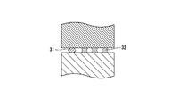
- FIG. 1 is a cross-sectional view schematically showing between opposing terminals before crimping.
- FIG. 2 is a cross-sectional view schematically showing between terminals facing each other after crimping.
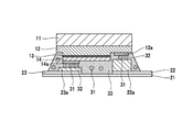
- FIG. 3 is a cross-sectional view showing an example of an LED mounting body according to an embodiment of the present invention.
- FIG. 4 is a cross-sectional view showing an example of an LED mounting body according to another embodiment of the present invention.
- FIG. 5 is a graph showing the thermal resistance value with respect to the blending amount of solder particles.
- FIG. 6 is a cross-sectional view showing an example of an LED mounting body by a wire bond method.
- FIG. 7 is a cross-sectional view showing an example of an LED mounting body using a conductive paste.
- FIG. 8 is a cross-sectional view showing an example of an LED mounting body using an anisotropic conductive adhesive.
- FIG. 9 is a cross-sectional view showing an example of an LED mounting body in which an FC mounting LED is mounted by gold-tin eutectic bonding.
- FIG. 10 is a cross-sectional view illustrating an example of an LED mounting body in which an FC mounting LED is mounted using a conductive paste.
- FIG. 11 is a cross-sectional view showing an example of an LED mounting body in which an FC mounting LED is mounted with an anisotropic conductive adhesive.
- the anisotropic conductive adhesive in the present embodiment is a conductive particle in which a conductive metal layer is formed on the surface of resin particles and solder particles dispersed in a binder (adhesive component).
- the shape is a paste, a film, etc., and can be appropriately selected according to the purpose.
- FIG. 1 and FIG. 2 are cross-sectional views schematically showing the terminals facing each other before and after crimping, respectively.
- the conductive particles 31 and the solder particles 32 can be present between the terminals before the pressure bonding by adopting a configuration in which the anisotropic conductive adhesive is described later.
- bonding since the electroconductive particle 31 which uses the resin particle for a core material deform
- the solder particles 32 are crushed following the flat deformation of the conductive particles and are metal-bonded by soldering by heating, so that the area in contact with the terminals is increased, and heat dissipation and electrical characteristics can be improved. it can.
- the conductive particles of the resin core relieve stress generated due to the difference in thermal expansion between the substrate and the element, it is possible to prevent cracks from occurring in the solder joints and improve connection reliability.
- Conductive particles are coated with metal such as Au, Ni, Zn on the surface of resin particles such as epoxy resin, phenol resin, acrylic resin, acrylonitrile / styrene (AS) resin, benzoguanamine resin, divinylbenzene resin, styrene resin, etc.
- resin particles such as epoxy resin, phenol resin, acrylic resin, acrylonitrile / styrene (AS) resin, benzoguanamine resin, divinylbenzene resin, styrene resin, etc.
- Metal-coated resin particles Since the metal-coated resin particles are easily crushed and easily deformed during compression, the contact area with the wiring pattern can be increased, and variations in the height of the wiring pattern can be absorbed.
- the blending amount of the conductive particles is preferably 1 to 30% by volume with respect to the binder from the viewpoint of connection reliability and insulation reliability.
- the average particle diameter (D50) of the conductive particles is preferably 1 to 10 ⁇ m, more preferably 2 to 6 ⁇ m.
- the solder particles are, for example, Sn—Pb, Pb—Sn—Sb, Sn—Sb, Sn—Pb—Bi, Bi—Sn, Sn—Cu, Sn, Cu, JISZ 3282-1999. It can be appropriately selected from —Pb—Cu, Sn—In, Sn—Ag, Sn—Pb—Ag, Pb—Ag, and the like according to the electrode material, connection conditions, and the like. Further, the shape of the solder particles can be appropriately selected from granular, flake shaped, and the like. Note that the solder particles may be covered with an insulating layer in order to improve anisotropy.
- the amount of solder particles is preferably 1 to 30% by volume. If the blending amount of the solder particles is too small, excellent heat dissipation cannot be obtained, and if the blending amount is too large, anisotropy is impaired and connection reliability cannot be obtained.
- the average particle size (D50) of the solder particles is preferably 25 to 400% of the average particle size of the conductive particles. If the solder particles are too small with respect to the conductive particles, the solder particles are not captured between the terminals facing each other at the time of pressure bonding, and good solder bonding is not performed, so that excellent heat dissipation cannot be obtained. On the other hand, if the solder particles are too large relative to the conductive particles, the anisotropy is impaired and connection reliability cannot be obtained.
- an adhesive composition used in a conventional anisotropic conductive adhesive or anisotropic conductive film can be used.
- Preferred examples of the adhesive composition include an epoxy curable adhesive mainly composed of an alicyclic epoxy compound, a heterocyclic epoxy compound, a hydrogenated epoxy compound, or the like.
- Preferred examples of the alicyclic epoxy compound include those having two or more epoxy groups in the molecule. These may be liquid or solid. Specific examples include glycidyl hexahydrobisphenol A, 3,4-epoxycyclohexenylmethyl-3 ', 4'-epoxycyclohexene carboxylate, and the like. Among these, 3,4-epoxycyclohexenylmethyl-3 ′, 4′-epoxycyclohexenecarboxylate is preferred because it can ensure light transmission suitable for mounting LED elements on the cured product and is excellent in rapid curing. Can be preferably used.
- heterocyclic epoxy compound examples include an epoxy compound having a triazine ring, and particularly preferably 1,3,5-tris (2,3-epoxypropyl) -1,3,5-triazine-2,4, Mention may be made of 6- (1H, 3H, 5H) -trione.
- water-added epoxy compound hydrogenated products of the above-described alicyclic epoxy compounds and heterocyclic epoxy compounds, and other known hydrogenated epoxy resins can be used.
- the alicyclic epoxy compound, heterocyclic epoxy compound and hydrogenated epoxy compound may be used alone, but two or more kinds may be used in combination.
- other epoxy compounds may be used in combination as long as the effects of the present invention are not impaired.
- the curing agent examples include acid anhydrides, imidazole compounds, and dicyan.
- acid anhydrides that are difficult to discolor the cured product particularly alicyclic acid anhydride-based curing agents, can be preferably used.
- methylhexahydrophthalic anhydride etc. can be mentioned preferably.
- the amount of each used is an uncured epoxy compound if there is too little alicyclic acid anhydride curing agent. If the amount is too large, corrosion of the adherend material tends to be accelerated due to the influence of the excess curing agent. Therefore, the alicyclic acid anhydride curing agent is added to 100 parts by mass of the alicyclic epoxy compound.
- the ratio is preferably 80 to 120 parts by mass, more preferably 95 to 105 parts by mass.
- the anisotropic conductive adhesive having such a structure has high heat dissipation and high connection reliability because the conductive particles are flattened by pressing during crimping, and the solder particles are crushed and are metal-bonded by soldering by heating. Can be obtained.
- anisotropic conductive adhesive in the present embodiment can be manufactured by uniformly mixing the adhesive composition, conductive particles, and solder particles.
- connection structure and manufacturing method thereof> Next, a connection structure using the above-described anisotropic conductive adhesive will be described.
- the terminals of the first electronic component and the terminals of the second electronic component are electrically connected via conductive particles in which a conductive metal layer is formed on the surface of the resin particles.
- the solder particles having an average particle size smaller than the conductive particles are captured between the terminals of the first electronic component and the terminals of the second electronic component.
- a chip such as a driver IC (Integrated Circuit) or LED (Light Emitting) Diode) that generates heat is suitable.
- FIG. 3 is a cross-sectional view showing a configuration example of the LED mounting body.
- an LED element and a substrate are connected using an anisotropic conductive adhesive in which the above-described conductive particles and solder particles are dispersed in an adhesive component.
- the LED element includes, for example, a first conductive clad layer 12 made of, for example, n-GaN, an active layer 13 made of, for example, an In x Al y Ga 1-xy N layer, on an element substrate 11 made of, for example, sapphire, and a second conductivity type cladding layer 14 made of p-GaN, and has a so-called double heterostructure. Further, a first conductivity type electrode 12 a is provided on a part of the first conductivity type cladding layer 12, and a second conductivity type electrode 14 a is provided on a part of the second conductivity type cladding layer 14. When a voltage is applied between the first conductivity type electrode 12a and the second conductivity type electrode 14a of the LED element, carriers are concentrated on the active layer 13 and recombination causes light emission.
- the substrate includes a circuit pattern 22 for the first conductivity type and a circuit pattern 23 for the second conductivity type on the base material 21, and positions corresponding to the first conductivity type electrode 12a and the second conductivity type electrode 14a of the LED element. Each have an electrode 22a and an electrode 23a.
- conductive particles 31 and solder particles 32 are dispersed in a binder 33 as described above.
- the LED mounting body has the LED element terminals (electrodes 12 a, 14 a) and the substrate terminals (electrodes 22 a, 23 a) electrically connected via conductive particles 31.
- the terminals of the board and the terminals of the board are soldered together.
- the heat generated in the active layer 13 of the LED element can be efficiently released to the substrate side, the decrease in light emission efficiency can be prevented, and the life of the LED mounting body can be extended.
- the solder particles 32 are white or gray achromatic, the light from the active layer 13 is reflected and high brightness can be obtained.
- the LED element for flip chip mounting is designed such that the terminals (electrodes 12a, 14a) of the LED element are large due to the passivation 105, and therefore the terminals (electrodes 12a, 14a) of the LED element. ) And the terminals (circuit patterns 22 and 23) of the substrate, more conductive particles 31 and solder particles 32 are captured. Thereby, the heat generated in the active layer 13 of the LED element can be released to the substrate side more efficiently.
- the method for manufacturing a mounting body in the present embodiment includes an anisotropic conductive adhesive in which the conductive particles described above and solder particles having an average particle size smaller than the conductive particles are dispersed in an adhesive component.
- the first electronic component and the second electronic component are thermocompression-bonded between the terminals of the first electronic component and the second electronic component.
- the terminal of the first electronic component and the terminal of the second electronic component are electrically connected via the conductive particles, and the terminal of the first electronic component and the terminal of the second electronic component are connected.
- a connection structure in which the gaps are soldered can be obtained.
- the conductive particles are flattened by pressing at the time of pressure bonding, and the solder particles are crushed and are metal-bonded by soldering by heating. Increase, and high heat dissipation and high connection reliability can be obtained. Moreover, since the conductive particles of the resin core relieve stress generated due to the difference in thermal expansion between the substrate and the element, it is possible to prevent cracks from occurring in the solder joint.
- Example> Examples of the present invention will be described in detail below, but the present invention is not limited to these examples.
- the production of the anisotropic conductive adhesive was performed as follows.
- anisotropic conductive adhesive In an epoxy curing adhesive (epoxy resin (trade name: CEL2021P, manufactured by Daicel Chemical Industries, Ltd.) and acid anhydride (MeHHPA, trade name: MH700, manufactured by Shin Nippon Rika Co., Ltd.)) Conductive particles (product name: AUL705, manufactured by Sekisui Chemical Co., Ltd.) having a mean particle size (D50) of 5 ⁇ m coated with Au on the surface of crosslinked polystyrene resin particles and solder particles (trade name) having an average particle size (D50) of 5 ⁇ m : M707, manufactured by Senju Metal Industry Co., Ltd.) to produce an anisotropic conductive adhesive having thermal conductivity.
- epoxy curing adhesive epoxy curing adhesive
- epoxy resin trade name: CEL2021P, manufactured by Daicel Chemical Industries, Ltd.
- Acid anhydride MeHHPA, trade name: MH700, manufactured by Shin Nippon Rika Co., Ltd.
- Conductive particles product name
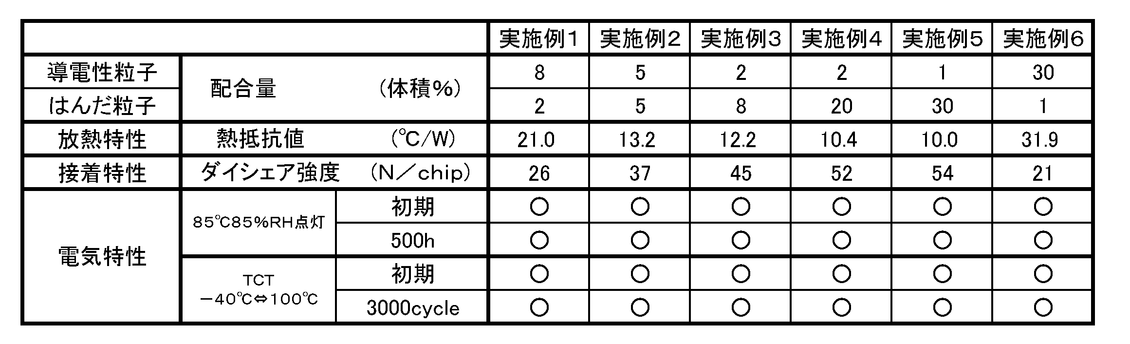
- Example 1 An anisotropic conductive adhesive having thermal conductivity was prepared by blending 8% by volume of conductive particles and 2% by volume of solder particles with the resin composition described above.
- the measurement result of the thermal resistance of the LED mounting body produced using this anisotropic conductive adhesive was 21.0 ° C./W, and the die shear strength was 26 N / chip.
- the evaluation result of the high-temperature and high-humidity test for electrical characteristics was ⁇ in the initial stage and ⁇ after the test, and the evaluation result of the thermal shock test for electrical characteristics was ⁇ in the initial stage and ⁇ after the test.
- Example 2 An anisotropic conductive adhesive having thermal conductivity was prepared by blending 5% by volume of conductive particles and 5% by volume of solder particles with the above resin composition.
- the measurement results of the thermal resistance of the LED package manufactured using this anisotropic conductive adhesive were 13.2 ° C./W, and the die shear strength was 37 N / chip.
- the evaluation result of the high-temperature and high-humidity test for electrical characteristics was ⁇ in the initial stage and ⁇ after the test, and the evaluation result of the thermal shock test for electrical characteristics was ⁇ in the initial stage and ⁇ after the test.
- Example 3 An anisotropic conductive adhesive having thermal conductivity was prepared by blending 2% by volume of conductive particles and 8% by volume of solder particles with the resin composition described above.
- the measurement result of the thermal resistance of the LED mounting body produced using this anisotropic conductive adhesive was 12.2 ° C./W, and the die shear strength was 45 N / chip.
- the evaluation result of the high-temperature and high-humidity test for electrical characteristics was ⁇ in the initial stage and ⁇ after the test, and the evaluation result of the thermal shock test for electrical characteristics was ⁇ in the initial stage and ⁇ after the test.
- Example 4 An anisotropic conductive adhesive having thermal conductivity was prepared by blending 2% by volume of conductive particles and 20% by volume of solder particles with the above resin composition.
- the measurement result of the thermal resistance of the LED mounting body produced using this anisotropic conductive adhesive was 10.4 ° C./W, and the die shear strength was 52 N / chip.
- the evaluation result of the high-temperature and high-humidity test for electrical characteristics was ⁇ in the initial stage and ⁇ after the test, and the evaluation result of the thermal shock test for electrical characteristics was ⁇ in the initial stage and ⁇ after the test.
- Example 5 An anisotropic conductive adhesive having thermal conductivity was prepared by blending 1% by volume of conductive particles and 30% by volume of solder particles with the above resin composition.
- the measurement result of the thermal resistance of the LED mounting body produced using this anisotropic conductive adhesive was 10.0 ° C./W, and the die shear strength was 54 N / chip.
- the evaluation result of the high-temperature and high-humidity test for electrical characteristics was ⁇ in the initial stage and ⁇ after the test, and the evaluation result of the thermal shock test for electrical characteristics was ⁇ in the initial stage and ⁇ after the test.
- Example 6 An anisotropic conductive adhesive having thermal conductivity was prepared by blending 30% by volume of conductive particles and 1% by volume of solder particles with the above resin composition.
- the measurement result of the thermal resistance of the LED mounting body produced using this anisotropic conductive adhesive was 31.9 ° C./W, and the die shear strength was 21 N / chip.
- the evaluation result of the high-temperature and high-humidity test for electrical characteristics was ⁇ in the initial stage and ⁇ after the test, and the evaluation result of the thermal shock test for electrical characteristics was ⁇ in the initial stage and ⁇ after the test.
- An anisotropic conductive adhesive having thermal conductivity was prepared by blending 10% by volume of solder particles without blending conductive particles with the resin composition described above.
- the measurement result of the thermal resistance of the LED mounting body produced using this anisotropic conductive adhesive was 11.8 ° C./W, and the die shear strength was 48 N / chip.
- the evaluation result of the electrical property high temperature and high humidity test was ⁇ at the initial stage and ⁇ after the test, and the evaluation result of the thermal shock test of the electrical property was ⁇ at the initial stage and ⁇ after the test.
- An anisotropic conductive adhesive having thermal conductivity was prepared by blending 40% by volume of solder particles without blending conductive particles into the resin composition described above.
- the die mounting strength of the LED mounting body manufactured using this anisotropic conductive adhesive was 55 N / chip.
- the evaluation result of the high temperature and high humidity test for electrical characteristics was ⁇ in the initial stage, and the evaluation result of the thermal shock test for electrical characteristics was ⁇ in the initial stage.
- FIG. 5 shows the thermal resistance value with respect to the amount of solder particles.
- FIG. 5 is a plot of the thermal resistance value versus the blending amount of the solder particles of Examples 1 to 6 and Comparative Examples 1 and 2.
- the thermal resistance value of the LED mounting body using ACP in which 8% by volume of conductive particles and 2% by volume of solder particles are added to the binder resin is 21.0 (° C./W).
- the thermal resistance value could be lowered as compared with Comparative Example 2 in which no solder particles were added, and the heat dissipation characteristics of the LED package were improved.
- the die shear strength was 26 N / chip, which was improved as compared with Comparative Example 2.
- the electrical connection reliability was good in the test 500 h.
- the electrical connection reliability was good even after the thermal shock test 3000 cycles.
- the thermal resistance value of the LED package using ACP in which 5% by volume of conductive particles and 5% by volume of solder particles are added to the binder resin is 13.2 (° C./W).
- the thermal resistance value could be lowered as compared with Comparative Example 2 in which no solder particles were added, and the heat dissipation characteristics of the LED package were improved.
- the die shear strength was 37 N / chip, which was improved as compared with Comparative Example 2.
- the electrical connection reliability was good in the test 500 h.
- the electrical connection reliability was good even after the thermal shock test 3000 cycles.
- the thermal resistance value of the LED mounting body using ACP in which 2% by volume of conductive particles and 8% by volume of solder particles are added to the binder resin is 12.2 (° C./W).
- the thermal resistance value could be lowered as compared with Comparative Example 2 in which no solder particles were added, and the heat dissipation characteristics of the LED package were improved.
- the die shear strength was 45 N / chip, which was improved as compared with Comparative Example 2.
- the electrical connection reliability was good in the test 500 h.
- the electrical connection reliability was good even after the thermal shock test 3000 cycles.
- the thermal resistance value of the LED mounting body using ACP in which 2% by volume of conductive particles and 20% by volume of solder particles are added to the binder resin is 10.4 (° C./W).
- the thermal resistance value could be lowered as compared with Comparative Example 2 in which no solder particles were added, and the heat dissipation characteristics of the LED package were improved.
- the die shear strength was 52 N / chip, which was improved as compared with Comparative Example 2.
- the electrical connection reliability was good in the test 500 h.
- the electrical connection reliability was good even after the thermal shock test 3000 cycles.
- the thermal resistance value of the LED package using ACP in which 1% by volume of conductive particles and 30% by volume of solder particles are added to the binder resin is 10.0 (° C./W).
- the thermal resistance value could be lowered as compared with Comparative Example 2 in which no solder particles were added, and the heat dissipation characteristics of the LED package were improved.
- the die shear strength was 54 N / chip, which was improved as compared with Comparative Example 2.
- the electrical connection reliability was good in the test 500 h.
- the electrical connection reliability was good even after the thermal shock test 3000 cycles.
- the thermal resistance value of the LED mounting body using ACP in which 30% by volume of conductive particles and 1% by volume of solder particles are added to the binder resin is 31.9 (° C./W).
- the thermal resistance value could be lowered as compared with Comparative Example 2 in which no solder particles were added, and the heat dissipation characteristics of the LED package were improved.
- the die shear strength was 21 N / chip, which was improved as compared with Comparative Example 2.
- the electrical connection reliability was good in the test 500 h.
- the electrical connection reliability was good even after the thermal shock test 3000 cycles.
- the thermal resistance value of the LED mounting sample using ACP in which 10% by volume of solder particles are added without adding conductive particles to the binder resin is 11.8 (° C./W).
- the thermal resistance value could be lowered as compared with Comparative Example 2 in which no solder particles were added, and the heat dissipation characteristics of the LED package were improved.
- the die shear strength was 48 N / chip, which was higher than that of Comparative Example 2.
- the electrical connection reliability was good in the test 500 h.
- OPEN was generated, and good electrical connection reliability could not be obtained.
- the LED mounting sample using ACP in which 8% by volume of conductive particles are added to the binder resin and no solder particles are added is stored under lighting in an environment of 85 ° C. and 85% RH.
- the electrical connection reliability was good at 500 hours of the test.
- the electrical connection reliability was good even after the thermal shock test 3000 cycles.
- the die shear strength was as low as 15 N / chip.
- the heat resistance value was 40.0 (° C./W), and good heat dissipation could not be obtained.
- solder particles and conductive particles in combination with the anisotropic conductive adhesive, it is possible to impart high heat dissipation to the LED package and to have high connection reliability.
- the agent could be obtained.
Landscapes
- Engineering & Computer Science (AREA)
- Mechanical Engineering (AREA)
- Chemical & Material Sciences (AREA)
- Organic Chemistry (AREA)
- Spectroscopy & Molecular Physics (AREA)
- Dispersion Chemistry (AREA)
- Physics & Mathematics (AREA)
- Manufacturing & Machinery (AREA)
- Microelectronics & Electronic Packaging (AREA)
- Wire Bonding (AREA)
- Adhesives Or Adhesive Processes (AREA)
- Led Device Packages (AREA)
- Conductive Materials (AREA)
- Electric Connection Of Electric Components To Printed Circuits (AREA)
- Non-Insulated Conductors (AREA)
Abstract
Description
本出願は、日本国において2012年9月24日に出願された日本特許出願番号特願2012-210224を基礎として優先権を主張するものであり、この出願は参照されることにより、本出願に援用される。
1.異方性導電接着剤及びその製造方法
2.接続構造体及びその製造方法
3.実施例
本実施の形態における異方性導電接着剤は、樹脂粒子の表面に導電性金属層が形成された導電性粒子と、はんだ粒子とがバインダー(接着剤成分)中に分散されたものであり、その形状は、ペースト、フィルムなどであり、目的に応じて適宜選択することができる。
次に、前述した異方性導電接着剤を用いた接続構造体について説明する。本実施の形態における接続構造体は、第1の電子部品の端子と、第2の電子部品の端子とが、樹脂粒子の表面に導電性金属層が形成された導電性粒子を介して電気的に接続されてなる接続構造体において、第1の電子部品の端子と前記第2の電子部品の端子との間に、導電性粒子よりも平均粒径が小さいはんだ粒子が捕捉されている。
以下、本発明の実施例について詳細に説明するが、本発明はこれらの実施例に限定されるものではない。
エポキシ硬化系接着剤(エポキシ樹脂(商品名:CEL2021P、(株)ダイセル化学製)及び酸無水物(MeHHPA、商品名:MH700、新日本理化(株)製)を主成分としたバインダー)中に、架橋ポリスチレン樹脂粒子の表面にAuが被覆された平均粒径(D50)5μmの導電性粒子(品名:AUL705、積水化学工業社製)と、平均粒径(D50)5μmのはんだ粒子(商品名:M707、千住金属工業社製)とを配合し、熱伝導性を有する異方性導電接着剤を作製した。
異方性導電接着剤を用いてFC実装用LEDチップ(商品名:DA700、CREE社製、Vf=3.2V(If=350mA))をAu電極基板(セラミック基板、導体スペース=100μmP、Ni/Auメッキ=5.0/0.3μm)に搭載した。異方性導電接着剤をAu電極基板に塗布した後、LEDチップをアライメントして搭載し、150℃/10秒→230℃-30秒、荷重1000g/chipの条件で加熱圧着を行った。
過渡熱抵抗測定装置(CATS電子設計社製)を用いて、LED実装体の熱抵抗値(℃/W)を測定した。測定条件はIf=350mA(定電流制御)で行った。
LED実装体の接着強度をダイショア強度測定器(PTR-1100:RHESCA社製)を用いて測定した。
初期Vf値として、If=350mA時のVf値を測定した。また、85℃、85%RH環境下でLED実装体をIf=350mAで500時間点灯させ(高温高湿試験)、If=350mA時のVf値を測定した。また、-40℃/30min<>100℃/30min、3000サイクルの熱衝撃試験に投入し、If=350mA時のVf値を測定した。
前述の樹脂組成物に導電性粒子を8体積%及びはんだ粒子を2体積%配合し、熱伝導性を有する異方性導電接着剤を作製した。この異方性導電接着剤を用いて作製したLED実装体の熱抵抗の測定結果は21.0℃/W、ダイシェア強度は26N/chipであった。また、電気特性の高温高湿試験の評価結果は、初期で○、試験後で○であり、電気特性の熱衝撃試験の評価結果は、初期で○、試験後で○であった。
前述の樹脂組成物に導電性粒子を5体積%及びはんだ粒子を5体積%配合し、熱伝導性を有する異方性導電接着剤を作製した。この異方性導電接着剤を用いて作製したLED実装体の熱抵抗の測定結果は13.2℃/W、ダイシェア強度は37N/chipであった。また、電気特性の高温高湿試験の評価結果は、初期で○、試験後で○であり、電気特性の熱衝撃試験の評価結果は、初期で○、試験後で○であった。
前述の樹脂組成物に導電性粒子を2体積%及びはんだ粒子を8体積%配合し、熱伝導性を有する異方性導電接着剤を作製した。この異方性導電接着剤を用いて作製したLED実装体の熱抵抗の測定結果は12.2℃/W、ダイシェア強度は45N/chipであった。また、電気特性の高温高湿試験の評価結果は、初期で○、試験後で○であり、電気特性の熱衝撃試験の評価結果は、初期で○、試験後で○であった。
前述の樹脂組成物に導電性粒子を2体積%及びはんだ粒子を20体積%配合し、熱伝導性を有する異方性導電接着剤を作製した。この異方性導電接着剤を用いて作製したLED実装体の熱抵抗の測定結果は10.4℃/W、ダイシェア強度は52N/chipであった。また、電気特性の高温高湿試験の評価結果は、初期で○、試験後で○であり、電気特性の熱衝撃試験の評価結果は、初期で○、試験後で○であった。
前述の樹脂組成物に導電性粒子を1体積%及びはんだ粒子を30体積%配合し、熱伝導性を有する異方性導電接着剤を作製した。この異方性導電接着剤を用いて作製したLED実装体の熱抵抗の測定結果は10.0℃/W、ダイシェア強度は54N/chipであった。また、電気特性の高温高湿試験の評価結果は、初期で○、試験後で○であり、電気特性の熱衝撃試験の評価結果は、初期で○、試験後で○であった。
前述の樹脂組成物に導電性粒子を30体積%及びはんだ粒子を1体積%配合し、熱伝導性を有する異方性導電接着剤を作製した。この異方性導電接着剤を用いて作製したLED実装体の熱抵抗の測定結果は31.9℃/W、ダイシェア強度は21N/chipであった。また、電気特性の高温高湿試験の評価結果は、初期で○、試験後で○であり、電気特性の熱衝撃試験の評価結果は、初期で○、試験後で○であった。
前述の樹脂組成物に導電性粒子を配合せずに、はんだ粒子を10体積%配合して熱伝導性を有する異方性導電接着剤を作製した。この異方性導電接着剤を用いて作製したLED実装体の熱抵抗の測定結果は11.8℃/W、ダイシェア強度は48N/chipであった。また、電気特性の高温高湿試験の評価結果は、初期で○、試験後で○であり、電気特性の熱衝撃試験の評価結果は、初期で○、試験後で×であった。
前述の樹脂組成物に導電性粒子を5体積%配合し、はんだ粒子を配合せずに熱伝導性を有する異方性導電接着剤を作製した。この異方性導電接着剤を用いて作製したLED実装体の熱抵抗の測定結果は40.0℃/W、ダイシェア強度は15N/chipであった。
また、電気特性の高温高湿試験の評価結果は、初期で○、試験後で○であり、電気特性の熱衝撃試験の評価結果は、初期で○、試験後で○であった。
前述の樹脂組成物に導電性粒子を配合せずに、はんだ粒子を40体積%配合して熱伝導性を有する異方性導電接着剤を作製した。この異方性導電接着剤を用いて作製したLED実装体のダイシェア強度は55N/chipであった。また、電気特性の高温高湿試験の評価結果は、初期で△であり、電気特性の熱衝撃試験の評価結果は、初期で△であった。
前述の樹脂組成物に導電性粒子を40体積%配合し、はんだ粒子を配合せずに熱伝導性を有する異方性導電接着剤を作製した。この異方性導電接着剤を用いて作製したLED実装体のダイシェア強度は15N/chipであった。また、電気特性の高温高湿試験の評価結果は、初期で△であり、電気特性の熱衝撃試験の評価結果は、初期で△であった。

Claims (6)
- 樹脂粒子の表面に導電性金属層が形成された導電性粒子と、はんだ粒子とが接着剤成分に分散されてなる異方性導電接着剤。
- 前記導電性粒子の配合量が、1~30体積%であり、
前記はんだ粒子の配合量が、1~30体積%である請求項1記載の異方性導電接着剤。 - 前記はんだ粒子の配合量が、5体積%以上である請求項2記載の異方性導電接着剤。
- 前記はんだ粒子の平均粒径が、前記導電性粒子の平均粒径の25~400%である請求項1乃至3のいずれか1項に記載の異方性導電接着剤。
- 第1の電子部品の端子と、第2の電子部品の端子とが、樹脂粒子の表面に導電性金属層が形成された導電性粒子を介して電気的に接続されてなる接続構造体において、
前記第1の電子部品の端子と前記第2の電子部品の端子との間が、はんだ接合されてなる接続構造体。 - 第1の電子部品が、LED素子であり、
第2の電子部品が、基板である請求項5記載の接続構造体。
Priority Applications (5)
| Application Number | Priority Date | Filing Date | Title |
|---|---|---|---|
| KR1020157009198A KR102159992B1 (ko) | 2012-09-24 | 2013-09-17 | 이방성 도전 접착제 |
| CN201380049646.2A CN104662118B (zh) | 2012-09-24 | 2013-09-17 | 各向异性导电粘接剂 |
| HK15110096.5A HK1209450A1 (en) | 2012-09-24 | 2013-09-17 | Anisotropic conductive adhesive |
| EP13840056.9A EP2899245B1 (en) | 2012-09-24 | 2013-09-17 | Anisotropic conductive adhesive |
| US14/423,887 US9676066B2 (en) | 2012-09-24 | 2013-09-17 | Anisotropic conductive adhesive |
Applications Claiming Priority (2)
| Application Number | Priority Date | Filing Date | Title |
|---|---|---|---|
| JP2012-210224 | 2012-09-24 | ||
| JP2012210224A JP2014065766A (ja) | 2012-09-24 | 2012-09-24 | 異方性導電接着剤 |
Publications (1)
| Publication Number | Publication Date |
|---|---|
| WO2014046093A1 true WO2014046093A1 (ja) | 2014-03-27 |
Family
ID=50341403
Family Applications (1)
| Application Number | Title | Priority Date | Filing Date |
|---|---|---|---|
| PCT/JP2013/075048 Ceased WO2014046093A1 (ja) | 2012-09-24 | 2013-09-17 | 異方性導電接着剤 |
Country Status (8)
| Country | Link |
|---|---|
| US (1) | US9676066B2 (ja) |
| EP (1) | EP2899245B1 (ja) |
| JP (1) | JP2014065766A (ja) |
| KR (1) | KR102159992B1 (ja) |
| CN (1) | CN104662118B (ja) |
| HK (1) | HK1209450A1 (ja) |
| TW (1) | TWI626293B (ja) |
| WO (1) | WO2014046093A1 (ja) |
Cited By (3)
| Publication number | Priority date | Publication date | Assignee | Title |
|---|---|---|---|---|
| WO2015056754A1 (ja) * | 2013-10-17 | 2015-04-23 | デクセリアルズ株式会社 | 異方性導電接着剤及び接続構造体 |
| CN106459717A (zh) * | 2014-05-23 | 2017-02-22 | 迪睿合株式会社 | 粘接剂及连接结构体 |
| EP3696866B1 (en) * | 2014-04-14 | 2023-11-01 | Nichia Corporation | Semiconductor device |
Families Citing this family (29)
| Publication number | Priority date | Publication date | Assignee | Title |
|---|---|---|---|---|
| JP6450923B2 (ja) * | 2013-12-20 | 2019-01-16 | パナソニックIpマネジメント株式会社 | 電子部品実装システムおよび電子部品実装方法ならびに電子部品実装装置 |
| JP6419457B2 (ja) * | 2014-05-23 | 2018-11-07 | デクセリアルズ株式会社 | 接着剤及び接続構造体 |
| JP6430148B2 (ja) * | 2014-05-23 | 2018-11-28 | デクセリアルズ株式会社 | 接着剤及び接続構造体 |
| CN107006131A (zh) * | 2014-07-28 | 2017-08-01 | 通用汽车环球科技运作有限责任公司 | 用于增强的粘合剂结合的系统和方法 |
| KR102055114B1 (ko) * | 2015-06-02 | 2019-12-12 | 데쿠세리아루즈 가부시키가이샤 | 접착제 조성물 |
| JP6519407B2 (ja) * | 2015-08-26 | 2019-05-29 | 日亜化学工業株式会社 | 発光装置及び発光装置の製造方法 |
| JP6710120B2 (ja) * | 2015-09-30 | 2020-06-17 | 太陽インキ製造株式会社 | 導電性接着剤、電子部品および電子部品の製造方法 |
| CN105336275A (zh) * | 2015-10-28 | 2016-02-17 | 江苏新广联半导体有限公司 | 高密rgb倒装led显示屏封装结构及制造方法 |
| CN106132086A (zh) * | 2016-07-08 | 2016-11-16 | 广东小天才科技有限公司 | 一种电路板结构及电子元件焊接方法 |
| CN105921909A (zh) * | 2016-07-18 | 2016-09-07 | 浙江亚通焊材有限公司 | 一种用于制备高温粘带纤料的粘结剂及高温粘带纤料 |
| JP2018088498A (ja) * | 2016-11-29 | 2018-06-07 | デクセリアルズ株式会社 | 異方性導電接着剤 |
| KR102555383B1 (ko) * | 2016-12-07 | 2023-07-12 | 엘지디스플레이 주식회사 | 유기발광소자를 이용한 조명장치 및 그 제조방법 |
| TWI761477B (zh) * | 2017-03-30 | 2022-04-21 | 日商太陽油墨製造股份有限公司 | 導電性接著劑、硬化物、電子零件及電子零件之製造方法 |
| TWI736695B (zh) * | 2017-10-24 | 2021-08-21 | 啟耀光電股份有限公司 | 電子裝置與其製造方法 |
| CN109728022B (zh) * | 2017-10-31 | 2023-06-20 | 英属开曼群岛商錼创科技股份有限公司 | 微型发光二极管显示面板及其制造方法 |
| TWI650854B (zh) * | 2017-10-31 | 2019-02-11 | 英屬開曼群島商錼創科技股份有限公司 | 微型發光二極體顯示面板及其製造方法 |
| KR101985499B1 (ko) * | 2017-12-28 | 2019-06-03 | 삼화콘덴서공업 주식회사 | 과전류 보호 기능을 가지는 금속 산화물 바리스터 |
| JP7185252B2 (ja) | 2018-01-31 | 2022-12-07 | 三国電子有限会社 | 接続構造体の作製方法 |
| JP7046351B2 (ja) | 2018-01-31 | 2022-04-04 | 三国電子有限会社 | 接続構造体の作製方法 |
| JP7160302B2 (ja) * | 2018-01-31 | 2022-10-25 | 三国電子有限会社 | 接続構造体および接続構造体の作製方法 |
| KR102769519B1 (ko) | 2018-02-14 | 2025-02-17 | 에피스타 코포레이션 | 발광 장치, 그 제조 방법 및 디스플레이 모듈 |
| TW202349704A (zh) * | 2018-02-14 | 2023-12-16 | 晶元光電股份有限公司 | 發光裝置、其製造方法及顯示模組 |
| CN110880544B (zh) * | 2018-09-06 | 2021-09-03 | 深圳市斯迈得半导体有限公司 | 一种用于玻璃基板的芯片及其制作方法 |
| CN110635017B (zh) * | 2019-08-09 | 2021-07-09 | 惠州市志金电子科技有限公司 | 一种miniled背光基板封装方法 |
| TWI819073B (zh) * | 2019-08-22 | 2023-10-21 | 晶元光電股份有限公司 | 發光裝置、其製造方法及顯示模組 |
| KR102270303B1 (ko) * | 2019-08-23 | 2021-06-30 | 삼성전기주식회사 | 적층형 커패시터 및 그 실장 기판 |
| CN111048499B (zh) * | 2019-12-16 | 2022-05-13 | 业成科技(成都)有限公司 | 微发光二极管显示面板及其制备方法 |
| US11901497B2 (en) * | 2019-12-24 | 2024-02-13 | Seoul Viosys Co., Ltd. | Method of repairing light emitting device, apparatus for repairing light emitting device, and display panel having repaired light emitting device |
| CN116631294A (zh) * | 2023-05-22 | 2023-08-22 | 业成科技(成都)有限公司 | 透明显示面板及其拼接方法 |
Citations (13)
| Publication number | Priority date | Publication date | Assignee | Title |
|---|---|---|---|---|
| JPS60178690A (ja) | 1984-02-24 | 1985-09-12 | ソニ−ケミカル株式会社 | 配線基板 |
| JPS6459786A (en) * | 1987-08-31 | 1989-03-07 | Hitachi Chemical Co Ltd | Connection member of circuit |
| JPH03129607A (ja) * | 1989-10-14 | 1991-06-03 | Sony Chem Corp | 異方性導電膜 |
| JPH04180029A (ja) * | 1990-11-15 | 1992-06-26 | Seiko Epson Corp | 回路の接続構造体 |
| JPH06187834A (ja) * | 1992-12-18 | 1994-07-08 | Sumitomo Bakelite Co Ltd | 異方導電フィルム |
| JPH08186156A (ja) | 1994-12-30 | 1996-07-16 | Casio Comput Co Ltd | 電子部品の接続方法 |
| JPH114064A (ja) | 1997-06-12 | 1999-01-06 | Nec Corp | 異方性導電樹脂及びこれを用いた電子部品の実装構造 |
| JPH11176879A (ja) | 1997-12-12 | 1999-07-02 | Citizen Watch Co Ltd | 半導体装置の実装方法およびこれに用いる異方性導電接着剤 |
| JPH11245082A (ja) * | 1997-12-29 | 1999-09-14 | Mitsui High Tec Inc | 電子部品の面実装用接続部材 |
| JP2006108523A (ja) * | 2004-10-08 | 2006-04-20 | Hitachi Chem Co Ltd | 異方性導電フィルムを用いた電気部品の接続方法 |
| JP2008072038A (ja) * | 2006-09-15 | 2008-03-27 | Matsushita Electric Ind Co Ltd | 電気部品の接続方法 |
| JP2013118181A (ja) * | 2011-11-02 | 2013-06-13 | Sekisui Chem Co Ltd | 異方性導電材料及び接続構造体 |
| JP2013118180A (ja) * | 2011-11-02 | 2013-06-13 | Sekisui Chem Co Ltd | 異方性導電材料及び接続構造体 |
Family Cites Families (8)
| Publication number | Priority date | Publication date | Assignee | Title |
|---|---|---|---|---|
| US5001542A (en) * | 1988-12-05 | 1991-03-19 | Hitachi Chemical Company | Composition for circuit connection, method for connection using the same, and connected structure of semiconductor chips |
| JPH08102218A (ja) * | 1994-09-30 | 1996-04-16 | Nec Corp | 異方性導電フィルム |
| US5965064A (en) * | 1997-10-28 | 1999-10-12 | Sony Chemicals Corporation | Anisotropically electroconductive adhesive and adhesive film |
| JP3119230B2 (ja) * | 1998-03-03 | 2000-12-18 | 日本電気株式会社 | 樹脂フィルムおよびこれを用いた電子部品の接続方法 |
| JP2002299378A (ja) * | 2001-03-30 | 2002-10-11 | Lintec Corp | 導電体付接着シート、半導体装置製造方法および半導体装置 |
| WO2006103918A1 (ja) * | 2005-03-28 | 2006-10-05 | Matsushita Electric Industrial Co., Ltd. | フリップチップ実装体とフリップチップ実装方法及びフリップチップ実装装置 |
| JP5499448B2 (ja) * | 2008-07-16 | 2014-05-21 | デクセリアルズ株式会社 | 異方性導電接着剤 |
| US10141084B2 (en) * | 2010-10-08 | 2018-11-27 | Cheil Industries, Inc. | Electronic device |
-
2012
- 2012-09-24 JP JP2012210224A patent/JP2014065766A/ja active Pending
-
2013
- 2013-09-17 EP EP13840056.9A patent/EP2899245B1/en active Active
- 2013-09-17 HK HK15110096.5A patent/HK1209450A1/xx unknown
- 2013-09-17 KR KR1020157009198A patent/KR102159992B1/ko active Active
- 2013-09-17 CN CN201380049646.2A patent/CN104662118B/zh active Active
- 2013-09-17 TW TW102133614A patent/TWI626293B/zh active
- 2013-09-17 WO PCT/JP2013/075048 patent/WO2014046093A1/ja not_active Ceased
- 2013-09-17 US US14/423,887 patent/US9676066B2/en active Active
Patent Citations (13)
| Publication number | Priority date | Publication date | Assignee | Title |
|---|---|---|---|---|
| JPS60178690A (ja) | 1984-02-24 | 1985-09-12 | ソニ−ケミカル株式会社 | 配線基板 |
| JPS6459786A (en) * | 1987-08-31 | 1989-03-07 | Hitachi Chemical Co Ltd | Connection member of circuit |
| JPH03129607A (ja) * | 1989-10-14 | 1991-06-03 | Sony Chem Corp | 異方性導電膜 |
| JPH04180029A (ja) * | 1990-11-15 | 1992-06-26 | Seiko Epson Corp | 回路の接続構造体 |
| JPH06187834A (ja) * | 1992-12-18 | 1994-07-08 | Sumitomo Bakelite Co Ltd | 異方導電フィルム |
| JPH08186156A (ja) | 1994-12-30 | 1996-07-16 | Casio Comput Co Ltd | 電子部品の接続方法 |
| JPH114064A (ja) | 1997-06-12 | 1999-01-06 | Nec Corp | 異方性導電樹脂及びこれを用いた電子部品の実装構造 |
| JPH11176879A (ja) | 1997-12-12 | 1999-07-02 | Citizen Watch Co Ltd | 半導体装置の実装方法およびこれに用いる異方性導電接着剤 |
| JPH11245082A (ja) * | 1997-12-29 | 1999-09-14 | Mitsui High Tec Inc | 電子部品の面実装用接続部材 |
| JP2006108523A (ja) * | 2004-10-08 | 2006-04-20 | Hitachi Chem Co Ltd | 異方性導電フィルムを用いた電気部品の接続方法 |
| JP2008072038A (ja) * | 2006-09-15 | 2008-03-27 | Matsushita Electric Ind Co Ltd | 電気部品の接続方法 |
| JP2013118181A (ja) * | 2011-11-02 | 2013-06-13 | Sekisui Chem Co Ltd | 異方性導電材料及び接続構造体 |
| JP2013118180A (ja) * | 2011-11-02 | 2013-06-13 | Sekisui Chem Co Ltd | 異方性導電材料及び接続構造体 |
Non-Patent Citations (1)
| Title |
|---|
| See also references of EP2899245A4 |
Cited By (6)
| Publication number | Priority date | Publication date | Assignee | Title |
|---|---|---|---|---|
| WO2015056754A1 (ja) * | 2013-10-17 | 2015-04-23 | デクセリアルズ株式会社 | 異方性導電接着剤及び接続構造体 |
| EP3696866B1 (en) * | 2014-04-14 | 2023-11-01 | Nichia Corporation | Semiconductor device |
| CN106459717A (zh) * | 2014-05-23 | 2017-02-22 | 迪睿合株式会社 | 粘接剂及连接结构体 |
| EP3147340A4 (en) * | 2014-05-23 | 2018-01-03 | Dexerials Corporation | Adhesive agent and connection structure |
| US10435601B2 (en) | 2014-05-23 | 2019-10-08 | Dexerials Corporation | Adhesive agent and connection structure |
| CN106459717B (zh) * | 2014-05-23 | 2021-01-15 | 迪睿合株式会社 | 粘接剂及连接结构体 |
Also Published As
| Publication number | Publication date |
|---|---|
| CN104662118A (zh) | 2015-05-27 |
| KR102159992B1 (ko) | 2020-09-25 |
| CN104662118B (zh) | 2017-08-18 |
| TW201412933A (zh) | 2014-04-01 |
| EP2899245B1 (en) | 2017-11-08 |
| US9676066B2 (en) | 2017-06-13 |
| HK1209450A1 (en) | 2016-04-01 |
| US20150209914A1 (en) | 2015-07-30 |
| KR20150060757A (ko) | 2015-06-03 |
| JP2014065766A (ja) | 2014-04-17 |
| TWI626293B (zh) | 2018-06-11 |
| EP2899245A4 (en) | 2016-06-01 |
| EP2899245A1 (en) | 2015-07-29 |
Similar Documents
| Publication | Publication Date | Title |
|---|---|---|
| WO2014046093A1 (ja) | 異方性導電接着剤 | |
| JP6066643B2 (ja) | 異方性導電接着剤 | |
| JP6176910B2 (ja) | 接続構造体の製造方法 | |
| JP6347635B2 (ja) | 異方性導電接着剤 | |
| WO2015056754A1 (ja) | 異方性導電接着剤及び接続構造体 | |
| JP2015088744A (ja) | 発光装置、異方性導電接着剤、発光装置製造方法 | |
| KR102368748B1 (ko) | 접착제 및 접속 구조체 | |
| TWI669721B (zh) | Anisotropic conductive adhesive | |
| JP6430148B2 (ja) | 接着剤及び接続構造体 | |
| JP2014065765A (ja) | 異方性導電接着剤 |
Legal Events
| Date | Code | Title | Description |
|---|---|---|---|
| 121 | Ep: the epo has been informed by wipo that ep was designated in this application |
Ref document number: 13840056 Country of ref document: EP Kind code of ref document: A1 |
|
| REEP | Request for entry into the european phase |
Ref document number: 2013840056 Country of ref document: EP |
|
| WWE | Wipo information: entry into national phase |
Ref document number: 14423887 Country of ref document: US |
|
| NENP | Non-entry into the national phase |
Ref country code: DE |
|
| ENP | Entry into the national phase |
Ref document number: 20157009198 Country of ref document: KR Kind code of ref document: A |