WO2014057760A1 - Ligne de signal haute fréquence - Google Patents
Ligne de signal haute fréquence Download PDFInfo
- Publication number
- WO2014057760A1 WO2014057760A1 PCT/JP2013/074650 JP2013074650W WO2014057760A1 WO 2014057760 A1 WO2014057760 A1 WO 2014057760A1 JP 2013074650 W JP2013074650 W JP 2013074650W WO 2014057760 A1 WO2014057760 A1 WO 2014057760A1
- Authority
- WO
- WIPO (PCT)
- Prior art keywords
- signal line
- ground conductor
- frequency signal
- axis direction
- adhesive layer
- Prior art date
- Legal status (The legal status is an assumption and is not a legal conclusion. Google has not performed a legal analysis and makes no representation as to the accuracy of the status listed.)
- Ceased
Links
Images






Classifications
-
- H—ELECTRICITY
- H01—ELECTRIC ELEMENTS
- H01P—WAVEGUIDES; RESONATORS, LINES, OR OTHER DEVICES OF THE WAVEGUIDE TYPE
- H01P3/00—Waveguides; Transmission lines of the waveguide type
- H01P3/02—Waveguides; Transmission lines of the waveguide type with two longitudinal conductors
- H01P3/08—Microstrips; Strip lines
- H01P3/081—Microstriplines
- H01P3/082—Multilayer dielectric
-
- H—ELECTRICITY
- H01—ELECTRIC ELEMENTS
- H01P—WAVEGUIDES; RESONATORS, LINES, OR OTHER DEVICES OF THE WAVEGUIDE TYPE
- H01P3/00—Waveguides; Transmission lines of the waveguide type
- H01P3/02—Waveguides; Transmission lines of the waveguide type with two longitudinal conductors
- H01P3/08—Microstrips; Strip lines
- H01P3/085—Triplate lines
-
- H—ELECTRICITY
- H04—ELECTRIC COMMUNICATION TECHNIQUE
- H04M—TELEPHONIC COMMUNICATION
- H04M1/00—Substation equipment, e.g. for use by subscribers
- H04M1/72—Mobile telephones; Cordless telephones, i.e. devices for establishing wireless links to base stations without route selection
- H04M1/725—Cordless telephones
-
- H—ELECTRICITY
- H01—ELECTRIC ELEMENTS
- H01P—WAVEGUIDES; RESONATORS, LINES, OR OTHER DEVICES OF THE WAVEGUIDE TYPE
- H01P3/00—Waveguides; Transmission lines of the waveguide type
- H01P3/02—Waveguides; Transmission lines of the waveguide type with two longitudinal conductors
- H01P3/06—Coaxial lines
Definitions
- the present invention relates to a high-frequency signal line, and more particularly to a high-frequency signal line used for transmission of a high-frequency signal.
- the signal line includes a laminate, a signal line, and two ground conductors.
- the laminate is configured by laminating a plurality of insulating sheets.
- the signal line is provided in the stacked body.
- the two ground conductors sandwich the signal line from the stacking direction in the stack. As a result, the signal line and the two ground conductors form a triplate stripline structure.
- the ground conductor is provided with a plurality of openings that overlap with the signal lines when viewed in plan from the stacking direction. This makes it difficult to form a capacitor between the signal line and the ground conductor at a position overlapping the opening. Therefore, the distance in the stacking direction between the signal line and the ground conductor can be reduced without making the characteristic impedance of the signal line too small. As a result, it is possible to reduce the thickness of the high-frequency signal line.
- the high-frequency signal line as described above is used for connecting two circuit boards.
- the signal line described in Patent Document 1 has a problem in that the distance between the signal line and the ground conductor varies depending on the condition when the laminated body is crimped. More specifically, in the crimping process of the signal line, a heating / pressurizing process is performed in a state where the insulating sheets are stacked. Thereby, the insulating sheet which consists of a liquid crystal polymer and a polyimide softens, and it integrates by what adjoins in the lamination direction.
- the degree to which the insulating sheet softens also varies.
- the thickness of the insulating sheet after the crimping process varies, and the distance between the signal line and the ground conductor varies.
- an object of the present invention is to provide a high-frequency signal line that can suppress the occurrence of variations in the distance between the signal line and the reference ground conductor.
- a high-frequency signal line is a dielectric in which a first dielectric layer, an adhesive layer, and a second dielectric layer are stacked so that they are arranged in this order from one side to the other side in the stacking direction.
- An element body, a linear signal line fixed to one main surface in the stacking direction of the adhesive layer, and a reference provided on one main surface in the stacking direction of the first dielectric layer A ground conductor and an auxiliary ground conductor provided on the second dielectric layer, and the adhesive layer adheres the first dielectric layer and the second dielectric layer.
- the distance between the signal line and the reference ground conductor in the stacking direction is larger than the distance between the signal line and the auxiliary ground conductor in the stacking direction.
- FIG. 4 is a cross-sectional structure diagram along AA in FIG. 3.
- FIG. 4 is a cross-sectional structure diagram along BB in FIG. 3.
- FIG. 1 is an external perspective view of a high-frequency signal transmission line 10 according to an embodiment of the present invention.
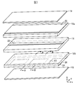
- FIG. 2 is an exploded view of the laminate 12 of the high-frequency signal transmission line 10 of FIG.
- FIG. 3 is an exploded perspective view of the line portion 12 a of the high-frequency signal line 10.
- FIG. 4 is a sectional structural view taken along line AA in FIG.
- FIG. 5 is a cross-sectional structural view taken along line BB in FIG.
- the stacking direction of the high-frequency signal transmission line 10 is defined as the z-axis direction.
- the longitudinal direction of the high-frequency signal transmission line 10 is defined as the x-axis direction, and the direction orthogonal to the x-axis direction and the z-axis direction is defined as the y-axis direction.
- the high-frequency signal line 10 is a flat cable used for connecting two high-frequency circuits in an electronic device such as a mobile phone. As shown in FIGS. 1 to 3, the high-frequency signal line 10 includes a dielectric body 12, external terminals 16a and 16b, a signal line 20, a reference ground conductor 22, an auxiliary ground conductor 24, via-hole conductors b1, b2, B1 to B6 and connectors 100a and 100b are provided.
- the dielectric body 12 is a flexible plate-like member that extends in the x-axis direction when viewed in plan from the z-axis direction, and includes a line portion 12 a, a connection portion 12 b, 12c is included.
- the dielectric body 12 includes a protective layer 14, a dielectric sheet 18 a, an adhesive layer 19, a dielectric sheet 18 b, and a protective layer 15, from the positive side in the z-axis direction to the negative side. It is the laminated body comprised by laminating
- the main surface on the positive side in the z-axis direction of the dielectric body 12 is referred to as the front surface
- the main surface on the negative direction side in the z-axis direction of the dielectric body 12 is referred to as the back surface.
- the line portion 12a extends in the x-axis direction.
- the connecting portions 12b and 12c are respectively connected to the negative end portion in the x-axis direction and the positive end portion in the x-axis direction of the line portion 12a, and have a rectangular shape.
- the width in the y-axis direction of the connection parts 12b and 12c is larger than the width in the y-axis direction of the line part 12a.
- the dielectric sheets 18 a and 18 b extend in the x-axis direction when viewed in plan from the z-axis direction, and have the same shape as the dielectric body 12.
- the dielectric sheets 18a and 18b are sheets made of a flexible thermoplastic resin such as polyimide or liquid crystal polymer.
- the front surface the main surface on the positive side in the z-axis direction of the dielectric sheets 18a and 18b
- the main surface on the negative direction side in the z-axis direction of the dielectric sheets 18a and 18b is referred to as the back surface.
- the adhesive layer 19 extends in the x-axis direction when viewed in plan from the z-axis direction, and has the same shape as the dielectric body 12.
- the adhesive layer 19 is a sheet made of a flexible thermoplastic resin such as polyimide or liquid crystal polymer. That is, the adhesive layer 19 is made of the same material as the dielectric sheets 18a and 18b.
- the softening start temperature of the adhesive layer 19 is lower than the softening start temperature of the dielectric sheets 18a and 18b. In the present embodiment, the softening start temperature of the adhesive layer 19 is 250 ° C., for example, and the softening start temperature of the dielectric sheets 18a and 18b is 280 ° C., for example.
- the adhesive layer 19 bonds the dielectric sheet 18a and the dielectric sheet 18b.
- the main surface on the positive side in the z-axis direction of the adhesive layer 19 is referred to as a front surface
- the main surface on the negative direction side in the z-axis direction of the adhesive layer 19 is referred to as a back surface.
- the thickness D1 of the dielectric sheet 18a is larger than the sum of the thickness D2 of the dielectric sheet 18b and the thickness D3 of the adhesive layer 19 as shown in FIGS.
- the thickness D1 is, for example, 50 ⁇ m to 300 ⁇ m.
- the thickness D1 is 150 ⁇ m.
- the total of the thickness D2 and the thickness D3 is, for example, 10 ⁇ m to 100 ⁇ m.
- the sum of the thickness D2 and the thickness D3 is 50 ⁇ m.
- the thickness D2 is 20 ⁇ m.
- the thickness D3 is 30 ⁇ m.
- the dielectric sheet 18a includes a line portion 18a-a and connecting portions 18a-b and 18a-c.
- the adhesive layer 19 includes a line portion 19-a and connection portions 19-b and 19-c.
- the dielectric sheet 18b includes a line portion 18b-a and connection portions 18b-b and 18b-c.
- the line portions 18a-a, 19-a, and 18b-a constitute the line portion 12a.
- the connecting portions 18a-b, 19-b, and 18b-b constitute a connecting portion 12b.
- the connecting portions 18a-c, 19-c, and 18b-c constitute a connecting portion 12c.
- the signal line 20 is a conductor that transmits a high-frequency signal and is provided in the dielectric body 12 as shown in FIGS. 2 and 3.
- the signal line 20 is a linear conductor that is formed on the surface of the adhesive layer 19 and extends in the x-axis direction. Thereby, the signal line 20 is fixed to the surface of the adhesive layer 19.
- adheresion includes those that are difficult to move from the surface of the adhesive layer 19 due to the anchor effect.
- the end of the signal line 20 on the negative direction side in the x-axis direction is located at the center of the connecting portion 19-b as shown in FIG. As shown in FIG.
- the signal line 20 is made of a metal material having a small specific resistance mainly composed of silver or copper.
- the signal line 20 is formed on the surface of the adhesive layer 19 means that the signal line 20 is formed by patterning a metal foil formed by plating on the surface of the adhesive layer 19, or the adhesive layer. This indicates that the signal line 20 is formed by patterning the metal foil attached to the surface of 19.
- the surface roughness of the surface of the signal line 20 that is in contact with the adhesive layer 19 is the surface roughness of the surface of the signal line 20 that is not in contact with the adhesive layer 19. It will be bigger than that.
- the surface roughness refers to the arithmetic average roughness Ra defined in JIS B 0601-2001 (based on ISO 4287-1997), and the same shall apply hereinafter.
- the reference ground conductor 22 is a solid conductor layer provided on the positive side in the z-axis direction from the signal line 20 as shown in FIGS. More specifically, the reference ground conductor 22 is formed on the surface of the dielectric sheet 18a and faces the signal line 20 via the dielectric sheet 18a. The reference ground conductor 22 is not provided with an opening at a position overlapping the signal line 20.
- the reference ground conductor 22 is made of a metal material having a small specific resistance mainly composed of silver or copper.
- the reference ground conductor 22 is formed on the surface of the dielectric sheet 18a. That is, the reference ground conductor 22 is formed by patterning a metal foil formed by plating on the surface of the dielectric sheet 18a.
- the reference ground conductor 22 is formed by patterning the metal foil attached to the surface of the dielectric sheet 18a. Further, since the surface of the reference ground conductor 22 is smoothed, as shown in FIGS. 4 and 5, the surface roughness of the surface of the reference ground conductor 22 that is in contact with the dielectric sheet 18a is the reference ground. It becomes larger than the surface roughness of the surface of the conductor 22 that is not in contact with the dielectric sheet 18a.
- the reference ground conductor 22 includes a line portion 22a and terminal portions 22b and 22c.
- the line portion 22a is provided on the surface of the line portion 18a-a and extends along the x-axis direction.
- the terminal portion 22b is provided on the surface of the line portion 18a-b and forms a rectangular ring.
- the terminal portion 22b is connected to the end portion on the negative direction side in the x-axis direction of the line portion 22a.
- the terminal portion 22c is provided on the surface of the connection portion 18a-c and forms a rectangular ring.
- the terminal portion 22c is connected to the end portion on the positive direction side in the x-axis direction of the line portion 22a.
- the auxiliary ground conductor 24 is a conductor layer provided on the negative side in the z-axis direction from the signal line 20. More specifically, the auxiliary ground conductor 24 is formed on the back surface of the dielectric sheet 18 b and faces the signal line 20 through the dielectric sheet 18 b and the adhesive layer 19.
- the auxiliary ground conductor 24 is made of a metal material having a small specific resistance mainly composed of silver or copper.
- the auxiliary ground conductor 24 is formed on the back surface of the dielectric sheet 18b means that the auxiliary ground conductor 24 is formed by patterning a metal foil formed by plating on the back surface of the dielectric sheet 18b.
- the auxiliary ground conductor 24 is formed by patterning the metal foil attached to the back surface of the dielectric sheet 18b. Further, since the surface of the auxiliary ground conductor 24 is smoothed, as shown in FIGS. 4 and 5, the surface roughness of the surface of the auxiliary ground conductor 24 that is in contact with the dielectric sheet 18b is the auxiliary ground conductor 24. It becomes larger than the surface roughness of the surface of the conductor 24 that is not in contact with the dielectric sheet 18b.
- the auxiliary ground conductor 24 includes a line portion 24a and terminal portions 24b and 24c.
- the line portion 24a is provided on the back surface of the line portion 18b-a and extends along the x-axis direction.
- the terminal portion 24b is provided on the back surface of the line portion 18b-b and forms a rectangular ring.
- the terminal portion 24b is connected to the end portion on the negative direction side in the x-axis direction of the line portion 24a.
- the terminal portion 24c is provided on the back surface of the connection portion 18b-c and forms a rectangular ring.
- the terminal portion 24c is connected to the end portion on the positive direction side in the x-axis direction of the line portion 24a.
- the line portion 24a is provided with a plurality of openings 30 that are arranged along the x-axis direction and have a rectangular shape.
- the line portion 24a has a ladder shape.
- a portion of the auxiliary ground conductor 24 sandwiched between adjacent openings 30 is referred to as a bridge portion 60.
- the bridge part 60 extends in the y-axis direction.
- the plurality of openings 30 and the plurality of bridge portions 60 alternately overlap the signal lines 20 when viewed in plan from the z-axis direction.
- the signal line 20 crosses the center of the opening 30 and the bridge portion 60 in the y-axis direction in the x-axis direction.
- the reference ground conductor 22 is not provided with an opening, and the auxiliary ground conductor 24 is provided with an opening. Therefore, the area where the reference ground conductor 22 and the signal line 20 overlap is larger than the area where the auxiliary ground conductor 24 and the signal line 20 overlap.
- the external terminal 16a is a rectangular conductor formed in the center on the surface of the connecting portion 18a-b. Therefore, the external terminal 16a overlaps the end of the signal line 20 on the negative direction side in the x-axis direction when viewed in plan from the z-axis direction.
- the external terminal 16b is a rectangular conductor formed at the center on the surface of the connecting portion 18a-c. Therefore, the external terminal 16b overlaps the end portion of the signal line 20 on the positive direction side in the x-axis direction when viewed in plan from the z-axis direction.
- the external terminals 16a and 16b are made of a metal material having a small specific resistance mainly composed of silver or copper.
- Ni / Au plating is applied to the surfaces of the external terminals 16a and 16b.
- the external terminals 16a and 16b are formed on the surface of the dielectric sheet 18a.
- the metal foil formed by plating on the surface of the dielectric sheet 18a is patterned to form the external terminals 16a and 16b. It indicates that the external terminals 16a and 16b are formed by patterning the metal foil attached to the surface of the dielectric sheet 18a. Since the surfaces of the external terminals 16a and 16b are smoothed, the surface roughness of the surface where the external terminals 16a and 16b are in contact with the dielectric sheet 18a is the same as that of the external terminals 16a and 16b. It becomes larger than the surface roughness of the non-contact surface.
- External terminals 16a and 16b, signal line 20, reference ground conductor 22 and auxiliary ground conductor 24 have substantially the same thickness.
- the thicknesses of the external terminals 16a and 16b, the signal line 20, the reference ground conductor 22, and the auxiliary ground conductor 24 are, for example, 10 ⁇ m to 20 ⁇ m.
- the signal line 20 is sandwiched between the reference ground conductor 22 and the auxiliary ground conductor 24 from both sides in the z-axis direction. That is, the signal line 20, the reference ground conductor 22, and the auxiliary ground conductor 24 have a triplate stripline structure. Further, the distance (distance in the z-axis direction) between the signal line 20 and the reference ground conductor 22 is substantially equal to the thickness D1 of the dielectric sheet 18a as shown in FIGS. 4 and 5, for example, 50 ⁇ m to 300 ⁇ m. . In the present embodiment, the distance between the signal line 20 and the reference ground conductor 22 is 150 ⁇ m.
- the distance between the signal line 20 and the auxiliary ground conductor 24 is the sum of the thickness D2 of the dielectric sheet 18b and the thickness D3 of the adhesive layer 19 as shown in FIGS. For example, they are 10 ⁇ m to 100 ⁇ m. In the present embodiment, the distance between the signal line 20 and the auxiliary ground conductor 24 is 50 ⁇ m. Therefore, the distance in the z-axis direction between the signal line 20 and the reference ground conductor 22 is larger than the distance in the z-axis direction between the signal line 20 and the auxiliary ground conductor 24.
- the plurality of via-hole conductors B1 pass through the dielectric sheet 18a in the z-axis direction on the positive side in the y-axis direction from the signal line 20, and are equally spaced in a line in the x-axis direction. Are lined up.
- the plurality of via-hole conductors B2 pass through the adhesive layer 19 in the z-axis direction on the positive side in the y-axis direction from the signal line 20, and are arranged at equal intervals in the x-axis direction. It is out. As shown in FIG.
- the plurality of via-hole conductors B3 pass through the dielectric sheet 18b in the z-axis direction on the positive side in the y-axis direction from the signal line 20, and are equally spaced in a line in the x-axis direction. Are lined up.
- the via hole conductors B1 to B3 are connected to each other to form one via hole conductor.
- the end of the via-hole conductor B1 on the positive side in the z-axis direction is connected to the reference ground conductor 22.
- the end of the via-hole conductor B3 on the negative side in the z-axis direction is connected to the auxiliary ground conductor 24.
- the via-hole conductor B3 is connected to the auxiliary ground conductor 24 on the positive side in the y-axis direction from the bridge portion 60.
- the via-hole conductors B1 to B3 are filled with a conductive paste mainly composed of silver, tin, copper, or the like in the via-holes formed in the dielectric sheet 18a, the adhesive layer 19, and the dielectric sheet 18b, and solidified. Formed by.
- the plurality of via-hole conductors B4 pass through the dielectric sheet 18a in the z-axis direction on the negative side in the y-axis direction from the signal line 20, and are evenly spaced in a line in the x-axis direction. Are lined up.
- the plurality of via-hole conductors B5 pass through the adhesive layer 19 in the z-axis direction on the negative side in the y-axis direction from the signal line 20, and are arranged at equal intervals in the x-axis direction. It is out. As shown in FIG.
- the plurality of via-hole conductors B6 pass through the dielectric sheet 18b in the z-axis direction on the negative side in the y-axis direction from the signal line 20, and are equally spaced in a line in the x-axis direction. Are lined up. Via-hole conductors B4 to B6 are connected to each other to form one via-hole conductor. The end of the via-hole conductor B4 on the positive side in the z-axis direction is connected to the reference ground conductor 22. The end of the via-hole conductor B6 on the negative side in the z-axis direction is connected to the auxiliary ground conductor 24.
- the via-hole conductor B6 is connected to the auxiliary ground conductor 24 on the negative direction side in the y-axis direction from the bridge portion 60.
- the via-hole conductors B4 to B6 are filled with a conductive paste mainly composed of silver, tin, copper, or the like in the via holes formed in the dielectric sheet 18a, the adhesive layer 19, and the dielectric sheet 18b, and solidified. Formed by.
- the via-hole conductor b1 passes through the dielectric sheet 18a in the z-axis direction, and connects the external terminal 16a and the end of the signal line 20 on the negative direction side in the x-axis direction.
- the via-hole conductor b2 passes through the dielectric sheet 18a in the z-axis direction, and connects the external terminal 16b and the end of the signal line 20 on the positive side in the x-axis direction. .
- the signal line 20 is connected between the external terminals 16a and 16b.
- the via-hole conductors b1 and b2 are formed by filling a via-hole formed in the dielectric sheet 18a with a conductive paste mainly composed of silver, tin, copper, or the like and solidifying it.
- the protective layer 14 is an insulating film that covers substantially the entire surface of the dielectric sheet 18a. Thereby, the protective layer 14 covers the reference ground conductor 22.
- the protective layer 14 is made of a flexible resin such as a resist material, for example.
- the protective layer 14 includes a line portion 14a and connecting portions 14b and 14c.
- the line portion 14a covers the line portion 22a by covering the entire surface of the line portion 18a-a.
- the connecting portion 14b is connected to the end portion on the negative side in the x-axis direction of the line portion 14a and covers the surface of the connecting portion 18a-b.
- openings Ha to Hd are provided in the connection portion 14b.
- the opening Ha is a rectangular opening provided in the center of the connection portion 14b.
- the external terminal 16a is exposed to the outside through the opening Ha.
- the opening Hb is a rectangular opening provided on the positive side in the y-axis direction with respect to the opening Ha.
- the opening Hc is a rectangular opening provided on the negative direction side in the x-axis direction from the opening Ha.
- the opening Hd is a rectangular opening provided on the negative side in the y-axis direction with respect to the opening Ha.
- the terminal portion 22b functions as an external terminal by being exposed to the outside through the openings Hb to Hd.
- the connecting portion 14c is connected to the end portion on the positive side in the x-axis direction of the line portion 14a and covers the surface of the connecting portion 18a-c.
- openings He to Hh are provided in the connection portion 14c.
- the opening He is a rectangular opening provided in the center of the connection portion 14c.
- the external terminal 16b is exposed to the outside through the opening He.
- the opening Hf is a rectangular opening provided on the positive direction side in the y-axis direction with respect to the opening He.
- the opening Hg is a rectangular opening provided closer to the positive direction side in the x-axis direction than the opening He.
- the opening Hh is a rectangular opening provided on the negative side in the y-axis direction with respect to the opening He.
- the terminal portion 22c functions as an external terminal by being exposed to the outside through the openings Hf to Hh.
- the protective layer 15 is an insulating film covering substantially the entire back surface of the dielectric sheet 18b. Thereby, the protective layer 15 covers the auxiliary ground conductor 24.
- the protective layer 15 is made of a flexible resin such as a resist material, for example.
- the characteristic impedance of the signal line 20 periodically varies between the impedance Z1 and the impedance Z2. More specifically, a relatively small capacitance is formed between the signal line 20 and the auxiliary ground conductor 24 in the section A1 that overlaps the opening 30 in the signal line 20. Therefore, the characteristic impedance of the signal line 20 in the section A1 is a relatively high impedance Z1.
- the characteristic impedance of the signal line 20 in the section A2 is a relatively low impedance Z2.
- the section A1 and the section A2 are alternately arranged in the x-axis direction. Therefore, the characteristic impedance of the signal line 20 periodically varies between the impedance Z1 and the impedance Z2.
- the impedance Z1 is, for example, 55 ⁇
- the impedance Z2 is, for example, 45 ⁇ .
- the average characteristic impedance of the entire signal line 20 is, for example, 50 ⁇ .
- FIG. 6 is an external perspective view of the connector 100 b of the high-frequency signal transmission line 10.
- FIG. 7 is a cross-sectional structure diagram of the connector 100 b of the high-frequency signal transmission line 10.
- the connector 100b includes a connector main body 102, external terminals 104 and 106, a central conductor 108, and an external conductor 110, as shown in FIGS.
- the connector main body 102 has a shape in which a cylindrical member is connected to a rectangular plate member, and is made of an insulating material such as a resin.
- the external terminal 104 is provided at a position facing the external terminal 16b on the negative side surface in the z-axis direction of the plate member of the connector main body 102.
- the external terminal 106 is provided at a position corresponding to the terminal portion 22c exposed through the openings Hf to Hh on the negative surface side in the z-axis direction of the plate member of the connector main body 102.
- the center conductor 108 is provided at the center of the cylindrical member of the connector main body 102 and is connected to the external terminal 104.
- the center conductor 108 is a signal terminal for inputting or outputting a high frequency signal.
- the external conductor 110 is provided on the inner peripheral surface of the cylindrical member of the connector main body 102 and is connected to the external terminal 106.
- the outer conductor 110 is a ground terminal that is maintained at a ground potential.
- the connector 100b configured as described above includes the connection portion 12c such that the external terminal 104 is connected to the external terminal 16b and the external terminal 106 is connected to the terminal portion 22c. Mounted on the surface. Thereby, the signal line 20 is electrically connected to the central conductor 108. Further, the reference ground conductor 22 and the auxiliary ground conductor 24 are electrically connected to the external conductor 110.
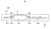
- FIG. 8 is a plan view of the electronic device 200 using the high-frequency signal transmission line 10 from the y-axis direction.
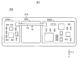
- FIG. 9 is a plan view of the electronic device 200 using the high-frequency signal transmission line 10 from the z-axis direction.
- the electronic device 200 includes the high-frequency signal line 10, circuit boards 202 a and 202 b, receptacles 204 a and 204 b, a battery pack (metal body) 206, and a housing 210.
- the circuit board 202a is provided with a transmission circuit or a reception circuit including an antenna, for example.
- a power supply circuit is provided on the circuit board 202b.
- the battery pack 206 is a lithium ion secondary battery, for example, and has a structure in which the surface is covered with a metal cover.
- the circuit board 202a, the battery pack 206, and the circuit board 202b are arranged in this order from the negative direction side to the positive direction side in the x-axis direction.
- the receptacles 204a and 204b are provided on the main surfaces of the circuit boards 202a and 202b on the negative side in the z-axis direction, respectively.
- Connectors 100a and 100b are connected to receptacles 204a and 204b, respectively.
- a high frequency signal having a frequency of, for example, 2 GHz transmitted between the circuit boards 202a and 202b is applied to the central conductor 108 of the connectors 100a and 100b via the receptacles 204a and 204b.
- the external conductor 110 of the connectors 100a and 100b is kept at the ground potential via the circuit boards 202a and 202b and the receptacles 204a and 204b.
- the high-frequency signal transmission line 10 connects between the circuit boards 202a and 202b.
- the surface of the dielectric body 12 (more precisely, the protective layer 14) is in contact with the battery pack 206.
- the dielectric body 12 and the battery pack 206 are fixed with an adhesive or the like.
- dielectric sheets 18a and 18b made of a thermoplastic resin having a copper foil (metal film) formed on the entire surface of one main surface are prepared. Specifically, a copper foil is attached to one main surface of the dielectric sheets 18a and 18b. Furthermore, the surface of the copper foil of the dielectric sheets 18a and 18b is smoothed by, for example, applying a zinc plating for rust prevention. Thereby, copper-clad dielectric sheets 18a and 18c having a non-fixed surface (shiny surface) with a small surface roughness and a fixed surface (matt surface) with a large surface roughness are obtained.
- the dielectric sheets 18a and 18b are liquid crystal polymers.
- the thickness of the copper foil is 10 ⁇ m to 20 ⁇ m.
- an adhesive layer 19 made of a thermoplastic resin having a copper foil (metal film) formed on the entire main surface is prepared. Specifically, a copper foil is attached to one main surface of the adhesive layer 19. Furthermore, the surface of the copper foil of the adhesive layer 19 is smoothed by applying, for example, zinc plating for rust prevention.
- the adhesive layer 19 is a liquid crystal polymer. The thickness of the copper foil is 10 ⁇ m to 20 ⁇ m.
- the external terminals 16a and 16b and the reference ground conductor 22 are formed on the surface of the dielectric sheet 18a as shown in FIG. .
- a resist having the same shape as the external terminals 16a and 16b and the reference ground conductor 22 shown in FIG. 2 is printed on the copper foil on the surface of the dielectric sheet 18a.
- the copper foil of the part which is not covered with the resist is removed by performing an etching process with respect to copper foil. Thereafter, a resist solution is sprayed to remove the resist.
- the external terminals 16a and 16b and the reference ground conductor 22 as shown in FIG. 2 are formed on the surface of the dielectric sheet 18a by a photolithography process.
- the signal line 20 is formed on the surface of the adhesive layer 19. Further, as shown in FIG. 2, the auxiliary ground conductor 24 is formed on the back surface of the dielectric sheet 18b.
- the process of forming the signal line 20 and the auxiliary ground conductor 24 is the same as the process of forming the external terminals 16a and 16b, the signal line 20 and the reference ground conductor 22, and thus the description thereof is omitted.
- through holes are formed by irradiating the dielectric sheets 18a and 18b and the positions where the via hole conductors b1, b2 and B1 to B6 of the adhesive layer 19 are formed with a laser beam. Then, the through holes are filled with a conductive paste to form via-hole conductors b1, b2, B1 to B6.
- the dielectric element body 12 is formed by stacking the dielectric sheet 18a, the adhesive layer 19 and the dielectric sheet 18b in this order from the positive direction side to the negative direction side in the z-axis direction.
- the dielectric sheet 18a, the adhesive layer 19 and the dielectric material are applied.
- the sheet 18b is crimped.
- the heating temperature is, for example, a temperature not lower than 250 ° C. and lower than 280.
- the dielectric sheets 18a and 18b are not softened, and only the adhesive layer 19 is softened.
- the dielectric sheets 18 a and 18 b are bonded by the adhesive layer 19.
- a protective layer 14 covering the reference ground conductor 22 is formed on the surface of the dielectric sheet 18a by applying a resin (resist) paste by screen printing.
- a protective layer 15 covering the auxiliary ground conductor 24 is formed on the back surface of the dielectric sheet 18b by applying a resin (resist) paste by screen printing.
- the connectors 100a and 100b are mounted on the external terminals 16a and 16b on the connection parts 12b and 12c and the terminal parts 22b and 22c by using solder. Thereby, the high frequency signal track 10 shown in FIG. 1 is obtained.
- the softening start temperature of the adhesive layer 19 is lower than the softening start temperature of the dielectric sheets 18a and 18b. Therefore, the temperature at the time of pressure bonding of the dielectric sheet 18a, the adhesive layer 19 and the dielectric sheet 18b is set to a temperature which is equal to or higher than the softening start temperature of the adhesive layer 19 and lower than the softening start temperature of the dielectric sheets 18a and 18b.
- the adhesive layer 19 is softened and the dielectric sheet 18a is not softened when the dielectric sheet 18a, the adhesive layer 19, and the dielectric sheet 18b are pressure-bonded.
- the signal line 20 is fixed on the surface of the adhesive layer 19, and the reference ground conductor 22 is provided on the surface of the dielectric sheet 18a.
- the softening of the dielectric sheet 18a suppresses the occurrence of variations in the distance between the signal line 20 and the reference ground conductor 22.
- the area where the reference ground conductor 22 and the signal line 20 overlap is larger than the area where the auxiliary ground conductor 24 and the signal line 20 overlap.
- the capacitance formed between the signal line 20 and the reference ground conductor 22 is larger than the capacitance formed between the signal line 20 and the auxiliary ground conductor 22. Therefore, when the variation in the distance between the signal line 20 and the reference ground conductor 22 is suppressed, the variation in the characteristic impedance of the signal line 20 is suppressed.
- the dielectric element body 12 can be thinned and desired electrical characteristics can be easily obtained. More specifically, in a general high-frequency signal line, as described above, in order to suppress the occurrence of variations in the distance between the ground conductor and the signal line, for example, using an adhesive layer, the dielectric sheets are connected to each other. It is conceivable to adhere these. The use of the adhesive layer eliminates the need to soften the dielectric sheet during pressure bonding. Thereby, the temperature at the time of crimping is lowered, and the dielectric sheet is not softened. As a result, the occurrence of variations in the distance between the signal line and the ground conductor is suppressed.
- a dielectric sheet on which signal lines are formed and a two-layer dielectric sheet on which two ground conductors are formed are required. That is, a three-layer dielectric sheet is required. For this reason, the thickness of the dielectric body is increased. Further, two adhesive layers are required to adhere the three dielectric sheets.
- the adhesive layer is greatly different from the dielectric sheet in characteristics such as dielectric constant, dielectric loss, and water absorption. For this reason, when the proportion of the adhesive layer included in the dielectric body increases, it becomes difficult to obtain desired electrical characteristics in the high-frequency signal line.
- the signal line 20 is formed on the adhesive layer 19. Therefore, the dielectric sheet on which the signal line 20 is formed becomes unnecessary, and only the two-layer dielectric sheets 18a and 18b are sufficient. As a result, in the high-frequency signal transmission line 10, the dielectric element body 12 can be thinned. In the high-frequency signal transmission line 10, only one adhesive layer 19 is provided. Therefore, in the high-frequency signal transmission line 10, desired electrical characteristics can be easily obtained.
- the dielectric sheets are connected to each other. It is conceivable to adhere these.
- a dielectric sheet in which a ground conductor is formed on one main surface and a signal line is formed on the other main surface is bonded to a two-layer dielectric sheet on which a ground conductor is formed by an adhesive layer. It is possible.
- the use of the adhesive layer eliminates the need to soften the dielectric sheet during pressure bonding. Thereby, the temperature at the time of crimping is lowered, and the dielectric sheet is not softened. As a result, the occurrence of variations in the distance between the signal line and the ground conductor is suppressed.
- the dielectric sheet in which a signal line is formed on one main surface and a ground conductor is formed on the other main surface it is necessary to use a dielectric sheet having copper foil formed on both main surfaces.
- the dielectric sheet in which the copper foil is formed on both main surfaces is harder than the dielectric sheet in which the copper foil is formed on one main surface.
- the patterning process of the signal line and the ground conductor is more complicated than the dielectric sheet in which the copper foil is formed on one main surface.
- the signal line 20 is formed on the adhesive layer 19. Therefore, the reference ground conductor 22 is formed on the surface of the dielectric sheet 18a, and the auxiliary ground conductor 24 is formed on the back surface of the dielectric sheet 18b. Therefore, in the high frequency signal transmission line 10, it is not necessary to use the dielectric sheet 18 in which the copper foil is formed on both main surfaces.
- the high-frequency signal transmission line 10 it is possible to reduce the thickness. More specifically, in the high-frequency signal transmission line 10, in the section A1, the signal line 20 does not overlap the auxiliary ground conductor 24 when viewed in plan from the z-axis direction. Therefore, it is difficult to form a capacitance between the signal line 20 and the auxiliary ground conductor 24. Therefore, even if the distance between the signal line 20 and the auxiliary ground conductor 24 in the z-axis direction is reduced, the capacitance formed between the signal line 20 and the auxiliary ground conductor 24 does not become too large. Therefore, the characteristic impedance of the signal line 20 is unlikely to deviate from a predetermined characteristic impedance (for example, 50 ⁇ ). As a result, according to the high-frequency signal transmission line 10, it is possible to reduce the thickness while maintaining the characteristic impedance of the signal line 20 at a predetermined characteristic impedance.
- a predetermined characteristic impedance for example, 50 ⁇
- the high-frequency signal line 10 when the high-frequency signal line 10 is attached to a metal body such as the battery pack 206, fluctuations in the characteristic impedance of the signal line 20 are suppressed. More specifically, the high-frequency signal line 10 is attached to the battery pack 206 so that the solid reference ground conductor 22 is located between the signal line 20 and the battery pack 206. As a result, the signal line 20 and the battery pack 206 do not face each other through the opening, and the formation of a capacity between the signal line 20 and the battery pack 206 is suppressed. As a result, the high-frequency signal line 10 is affixed to the battery pack 206, thereby suppressing the characteristic impedance of the signal line 20 from being lowered.
- FIG. 10 is an exploded view of the multilayer body 12 of the high-frequency signal transmission line 10a according to the modification.
- FIG. 11 is a cross-sectional structure diagram in the opening 30 of the high-frequency signal transmission line 10a.
- FIG. 12 is a cross-sectional structure diagram of the bridge portion 60 of the high-frequency signal transmission line 10a.
- FIG. 1 is used for an external perspective view of the high-frequency signal transmission line 10a.
- the high-frequency signal line 10a is different from the high-frequency signal line 10 in that the material of the adhesive layer 19 is different and through-hole conductors T1 to T4 are used. More specifically, in the high-frequency signal line 10a, the adhesive layer 19 is made of an epoxy-based thermosetting resin. The curing start temperature of the adhesive layer 19 is lower than the softening start temperature of the dielectric sheets 18a and 18b. As a result, the signal line 20 cannot be formed directly on the surface of the adhesive layer 19. Therefore, a rolled metal plate having a linear shape is used as the signal line 20. The signal line 20 is fixed to the surface of the adhesive layer 19.
- the signal line 20 is a rolled metal plate, the surface on the positive direction side in the z-axis direction and the surface on the negative direction side in the z-axis direction are smooth in the signal line 20 as shown in FIGS. is there. Therefore, the signal line 20 is bonded to the adhesive layer 19 by the adhesive force of the adhesive layer 19 and is not fixed by the anchor effect.
- thermosetting resin used for the adhesive layer 19
- a via-hole conductor cannot be formed. Therefore, in the high-frequency signal transmission line 10a, as shown in FIGS. 10 and 12, through-hole conductors T1 to T4 are formed.
- the plurality of through-hole conductors T1 penetrate the dielectric sheet 18a, the adhesive layer 19, and the dielectric sheet 18b in the z-axis direction on the positive side in the y-axis direction from the signal line 20. Are arranged at equal intervals in a line in the x-axis direction.
- the end of the through-hole conductor T1 on the positive side in the z-axis direction is connected to the reference ground conductor 22.
- the end of the through-hole conductor T1 on the negative direction side in the z-axis direction is connected to the auxiliary ground conductor 24.
- the through-hole conductor T1 connects the reference ground conductor 22 and the auxiliary ground conductor 24.
- a metal film mainly composed of nickel or gold is formed by plating on the inner peripheral surface of the through-hole penetrating the laminated dielectric sheet 18a, the adhesive layer 19, and the dielectric sheet 18b. Is formed by.
- the plurality of through-hole conductors T2 penetrate the dielectric sheet 18a, the adhesive layer 19, and the dielectric sheet 18b in the z-axis direction on the negative side in the y-axis direction from the signal line 20.
- the end of the through-hole conductor T2 on the positive side in the z-axis direction is connected to the reference ground conductor 22.
- the end of the through-hole conductor T2 on the negative side in the z-axis direction is connected to the auxiliary ground conductor 24.
- the through-hole conductor T2 connects the reference ground conductor 22 and the auxiliary ground conductor 24.
- a metal film mainly composed of nickel or gold is formed by plating on the inner peripheral surface of the through-hole penetrating the laminated dielectric sheet 18a, adhesive layer 19, and dielectric sheet 18b. Is formed by.
- the through-hole conductor T3 passes through the dielectric sheet 18a, the adhesive layer 19, and the dielectric sheet 18b in the z-axis direction, and the negative direction of the external terminal 16a and the signal line 20 in the x-axis direction.
- the end of the side is connected.
- the through-hole conductor T4 passes through the dielectric sheet 18a, the adhesive layer 19, and the dielectric sheet 18b in the z-axis direction, and the positive direction of the external terminal 16b and the signal line 20 in the x-axis direction.
- the end of the side is connected.
- the signal line 20 is connected between the external terminals 16a and 16b.
- a metal film mainly composed of nickel or gold is formed by plating on the inner peripheral surface of the through-hole penetrating the dielectric sheet 18a, the adhesive layer 19 and the dielectric sheet 18b after lamination. Is formed by.
- openings O1 and O2 are provided at positions overlapping the through-hole conductors T1 and T2.
- openings O3 to O6 are provided at positions overlapping with the through holes T1 to T4.
- the high-frequency signal transmission line 10 a configured as described above, it is possible to suppress the occurrence of variations in the distance between the signal line 20 and the reference ground conductor 22. More specifically, in the high-frequency signal line 10a, an adhesive layer 19 made of a thermosetting resin is used. The curing start temperature of the adhesive layer 19 is lower than the softening start temperature of the dielectric sheets 18a and 18b. Therefore, the temperature at the time of pressure bonding of the dielectric sheet 18a, the adhesive layer 19 and the dielectric sheet 18b is set to a temperature equal to or higher than the curing start temperature of the adhesive layer 19 and lower than the softening start temperature of the dielectric sheets 18a and 18b.
- the adhesive sheet 19 is cured by heating without softening the dielectric sheets 18a and 18b, and the dielectric sheets 18a and 18b. Can be bonded.
- the signal line 20 is fixed on the surface of the adhesive layer 19, and the reference ground conductor 22 is provided on the surface of the dielectric sheet 18a.
- the softening of the dielectric sheet 18a suppresses the occurrence of variations in the distance between the signal line 20 and the reference ground conductor 22.
- the area where the reference ground conductor 22 and the signal line 20 overlap is larger than the area where the auxiliary ground conductor 24 and the signal line 20 overlap. For this reason, the capacitance formed between the signal line 20 and the reference ground conductor 22 is larger than the capacitance formed between the signal line 20 and the auxiliary ground conductor 22. Therefore, if the occurrence of variation in the distance between the signal line 20 and the reference ground conductor 22 is suppressed, the occurrence of variation in the characteristic impedance of the signal line 20 is suppressed.
- the dielectric sheet 18b and the adhesive layer 19 positioned between the signal line 20 and the auxiliary ground conductor 24 are not softened by heating. Therefore, the occurrence of variations in the distance between the signal line 20 and the auxiliary ground conductor 24 is also suppressed.
- the dielectric element body 12 can be thinned and desired electrical characteristics can be easily obtained.
- the dielectric sheet 18 having copper foils formed on both main surfaces.
- the characteristic impedance of the signal line 20 may fluctuate. It is suppressed.
- the high-frequency signal line according to the present invention is not limited to the high-frequency signal lines 10 and 10a, and can be changed within the scope of the gist thereof.
- the protective layers 14 and 15 are formed by screen printing, but may be formed by a photolithography process.
- the connectors 100a and 100b may not be mounted on the high-frequency signal transmission lines 10 and 10a. In this case, the ends of the high-frequency signal transmission lines 10 and 10a and the circuit board are connected by solder. Note that the connector 100a may be mounted only on one end of the high-frequency signal transmission lines 10 and 10a.
- the connectors 100a and 100b are mounted on the front surface of the high-frequency signal lines 10 and 10a, but may be mounted on the back surface of the high-frequency signal lines 10 and 10a. Further, the connector 100a may be mounted on the surface of the high-frequency signal lines 10, 10a, and the connector 100b may be mounted on the back surface of the high-frequency signal lines 10, 10a.
- At least one of the reference ground conductor 22 and the auxiliary ground conductor 24 may not be provided.
- auxiliary ground conductor 24 may not have an opening.
- the auxiliary ground conductor 24 may be provided on the surface of the dielectric sheet 18b.
- the high-frequency signal lines 10 and 10a may be used as high-frequency signal lines in an RF circuit board such as an antenna front end module.
- the present invention is useful for a high-frequency signal line, and is particularly excellent in that variation in the distance between the signal line and the reference ground conductor can be suppressed.
Landscapes
- Engineering & Computer Science (AREA)
- Computer Networks & Wireless Communication (AREA)
- Signal Processing (AREA)
- Structure Of Printed Boards (AREA)
- Waveguides (AREA)
Priority Applications (3)
| Application Number | Priority Date | Filing Date | Title |
|---|---|---|---|
| CN201390000520.1U CN204361242U (zh) | 2012-10-12 | 2013-09-12 | 高频信号线路 |
| JP2014540785A JP5862790B2 (ja) | 2012-10-12 | 2013-09-12 | 高周波信号線路 |
| US14/547,374 US9490515B2 (en) | 2012-10-12 | 2014-11-19 | High-frequency signal line |
Applications Claiming Priority (2)
| Application Number | Priority Date | Filing Date | Title |
|---|---|---|---|
| JP2012226567 | 2012-10-12 | ||
| JP2012-226567 | 2012-10-12 |
Related Child Applications (1)
| Application Number | Title | Priority Date | Filing Date |
|---|---|---|---|
| US14/547,374 Continuation US9490515B2 (en) | 2012-10-12 | 2014-11-19 | High-frequency signal line |
Publications (1)
| Publication Number | Publication Date |
|---|---|
| WO2014057760A1 true WO2014057760A1 (fr) | 2014-04-17 |
Family
ID=50477231
Family Applications (1)
| Application Number | Title | Priority Date | Filing Date |
|---|---|---|---|
| PCT/JP2013/074650 Ceased WO2014057760A1 (fr) | 2012-10-12 | 2013-09-12 | Ligne de signal haute fréquence |
Country Status (4)
| Country | Link |
|---|---|
| US (1) | US9490515B2 (fr) |
| JP (1) | JP5862790B2 (fr) |
| CN (1) | CN204361242U (fr) |
| WO (1) | WO2014057760A1 (fr) |
Citations (3)
| Publication number | Priority date | Publication date | Assignee | Title |
|---|---|---|---|---|
| JPH11289204A (ja) * | 1991-08-21 | 1999-10-19 | General Electric Co <Ge> | マイクロ波装置 |
| JP2009016521A (ja) * | 2007-07-04 | 2009-01-22 | Nippon Mektron Ltd | マイクロストリップライン構造およびその製造方法 |
| WO2012074100A1 (fr) * | 2010-12-03 | 2012-06-07 | 株式会社村田製作所 | Circuit d'acheminement des signaux haute fréquence |
Family Cites Families (4)
| Publication number | Priority date | Publication date | Assignee | Title |
|---|---|---|---|---|
| JP2009032874A (ja) * | 2007-07-26 | 2009-02-12 | Toshiba Corp | プリント配線基板 |
| TWI379621B (en) * | 2007-08-02 | 2012-12-11 | Shinetsu Polymer Co | Conductive noise suppressing structure and wiring circuit substrate |
| KR101378027B1 (ko) | 2009-07-13 | 2014-03-25 | 가부시키가이샤 무라타 세이사쿠쇼 | 신호선로 및 회로기판 |
| JP5041108B2 (ja) | 2010-12-03 | 2012-10-03 | 株式会社村田製作所 | 高周波信号線路 |
-
2013
- 2013-09-12 JP JP2014540785A patent/JP5862790B2/ja active Active
- 2013-09-12 CN CN201390000520.1U patent/CN204361242U/zh not_active Expired - Lifetime
- 2013-09-12 WO PCT/JP2013/074650 patent/WO2014057760A1/fr not_active Ceased
-
2014
- 2014-11-19 US US14/547,374 patent/US9490515B2/en active Active
Patent Citations (3)
| Publication number | Priority date | Publication date | Assignee | Title |
|---|---|---|---|---|
| JPH11289204A (ja) * | 1991-08-21 | 1999-10-19 | General Electric Co <Ge> | マイクロ波装置 |
| JP2009016521A (ja) * | 2007-07-04 | 2009-01-22 | Nippon Mektron Ltd | マイクロストリップライン構造およびその製造方法 |
| WO2012074100A1 (fr) * | 2010-12-03 | 2012-06-07 | 株式会社村田製作所 | Circuit d'acheminement des signaux haute fréquence |
Also Published As
| Publication number | Publication date |
|---|---|
| US20150072725A1 (en) | 2015-03-12 |
| JPWO2014057760A1 (ja) | 2016-09-05 |
| US9490515B2 (en) | 2016-11-08 |
| CN204361242U (zh) | 2015-05-27 |
| JP5862790B2 (ja) | 2016-02-16 |
Similar Documents
| Publication | Publication Date | Title |
|---|---|---|
| JP5610110B1 (ja) | フレキシブル基板及び電子機器 | |
| JP5754554B2 (ja) | 高周波信号線路の製造方法 | |
| JP5765468B2 (ja) | 高周波信号線路 | |
| JP6146522B2 (ja) | 高周波信号伝送線路及び電子機器 | |
| JP2014086655A (ja) | フレキシブル基板 | |
| JP5472556B2 (ja) | 高周波信号線路及び電子機器 | |
| WO2014125988A1 (fr) | Ligne de transmission de signaux haute fréquence, appareil électronique et procédé de fabrication de ligne de transmission de signaux haute fréquence | |
| JP5704286B2 (ja) | 高周波信号線路 | |
| WO2014021372A1 (fr) | Câble plat | |
| JP5862774B2 (ja) | 高周波信号線路及び信号線路付き基材層の製造方法 | |
| JP5605528B2 (ja) | 高周波信号伝送線路及び電子機器 | |
| JP5862790B2 (ja) | 高周波信号線路 | |
| CN204230398U (zh) | 高频信号传输线路以及电子设备 | |
| JP5935620B2 (ja) | フラットケーブル | |
| JP5958122B2 (ja) | 高周波信号線路及び信号線路付き基材層の製造方法 | |
| WO2014065172A1 (fr) | Substrat flexible | |
| JP2014078836A (ja) | 高周波信号線路及びその製造方法 | |
| JP2014011046A (ja) | 信号線路付き基材層の製造方法及び高周波信号線路の製造方法 |
Legal Events
| Date | Code | Title | Description |
|---|---|---|---|
| WWE | Wipo information: entry into national phase |
Ref document number: 201390000520.1 Country of ref document: CN |
|
| 121 | Ep: the epo has been informed by wipo that ep was designated in this application |
Ref document number: 13845249 Country of ref document: EP Kind code of ref document: A1 |
|
| ENP | Entry into the national phase |
Ref document number: 2014540785 Country of ref document: JP Kind code of ref document: A |
|
| NENP | Non-entry into the national phase |
Ref country code: DE |
|
| 122 | Ep: pct application non-entry in european phase |
Ref document number: 13845249 Country of ref document: EP Kind code of ref document: A1 |