WO2014068811A1 - 半導体パッケージ及びその実装構造 - Google Patents
半導体パッケージ及びその実装構造 Download PDFInfo
- Publication number
- WO2014068811A1 WO2014068811A1 PCT/JP2013/003956 JP2013003956W WO2014068811A1 WO 2014068811 A1 WO2014068811 A1 WO 2014068811A1 JP 2013003956 W JP2013003956 W JP 2013003956W WO 2014068811 A1 WO2014068811 A1 WO 2014068811A1
- Authority
- WO
- WIPO (PCT)
- Prior art keywords
- semiconductor package
- probe
- layer
- protrusion
- pattern
- Prior art date
- Legal status (The legal status is an assumption and is not a legal conclusion. Google has not performed a legal analysis and makes no representation as to the accuracy of the status listed.)
- Ceased
Links
Images






Classifications
-
- H—ELECTRICITY
- H01—ELECTRIC ELEMENTS
- H01P—WAVEGUIDES; RESONATORS, LINES, OR OTHER DEVICES OF THE WAVEGUIDE TYPE
- H01P5/00—Coupling devices of the waveguide type
- H01P5/08—Coupling devices of the waveguide type for linking dissimilar lines or devices
- H01P5/10—Coupling devices of the waveguide type for linking dissimilar lines or devices for coupling balanced lines or devices with unbalanced lines or devices
- H01P5/107—Hollow-waveguide/strip-line transitions
-
- H—ELECTRICITY
- H10—SEMICONDUCTOR DEVICES; ELECTRIC SOLID-STATE DEVICES NOT OTHERWISE PROVIDED FOR
- H10W—GENERIC PACKAGES, INTERCONNECTIONS, CONNECTORS OR OTHER CONSTRUCTIONAL DETAILS OF DEVICES COVERED BY CLASS H10
- H10W44/00—Electrical arrangements for controlling or matching impedance
- H10W44/20—Electrical arrangements for controlling or matching impedance at high-frequency [HF] or radio frequency [RF]
-
- H—ELECTRICITY
- H10—SEMICONDUCTOR DEVICES; ELECTRIC SOLID-STATE DEVICES NOT OTHERWISE PROVIDED FOR
- H10W—GENERIC PACKAGES, INTERCONNECTIONS, CONNECTORS OR OTHER CONSTRUCTIONAL DETAILS OF DEVICES COVERED BY CLASS H10
- H10W70/00—Package substrates; Interposers; Redistribution layers [RDL]
- H10W70/60—Insulating or insulated package substrates; Interposers; Redistribution layers
-
- H—ELECTRICITY
- H10—SEMICONDUCTOR DEVICES; ELECTRIC SOLID-STATE DEVICES NOT OTHERWISE PROVIDED FOR
- H10W—GENERIC PACKAGES, INTERCONNECTIONS, CONNECTORS OR OTHER CONSTRUCTIONAL DETAILS OF DEVICES COVERED BY CLASS H10
- H10W70/00—Package substrates; Interposers; Redistribution layers [RDL]
- H10W70/60—Insulating or insulated package substrates; Interposers; Redistribution layers
- H10W70/62—Insulating or insulated package substrates; Interposers; Redistribution layers characterised by their interconnections
- H10W70/65—Shapes or dispositions of interconnections
-
- H—ELECTRICITY
- H10—SEMICONDUCTOR DEVICES; ELECTRIC SOLID-STATE DEVICES NOT OTHERWISE PROVIDED FOR
- H10W—GENERIC PACKAGES, INTERCONNECTIONS, CONNECTORS OR OTHER CONSTRUCTIONAL DETAILS OF DEVICES COVERED BY CLASS H10
- H10W70/00—Package substrates; Interposers; Redistribution layers [RDL]
- H10W70/60—Insulating or insulated package substrates; Interposers; Redistribution layers
- H10W70/67—Insulating or insulated package substrates; Interposers; Redistribution layers characterised by their insulating layers or insulating parts
- H10W70/68—Shapes or dispositions thereof
- H10W70/685—Shapes or dispositions thereof comprising multiple insulating layers
-
- H—ELECTRICITY
- H10—SEMICONDUCTOR DEVICES; ELECTRIC SOLID-STATE DEVICES NOT OTHERWISE PROVIDED FOR
- H10W—GENERIC PACKAGES, INTERCONNECTIONS, CONNECTORS OR OTHER CONSTRUCTIONAL DETAILS OF DEVICES COVERED BY CLASS H10
- H10W76/00—Containers; Fillings or auxiliary members therefor; Seals
- H10W76/10—Containers or parts thereof
- H10W76/12—Containers or parts thereof characterised by their shape
- H10W76/13—Containers comprising a conductive base serving as an interconnection
-
- H—ELECTRICITY
- H10—SEMICONDUCTOR DEVICES; ELECTRIC SOLID-STATE DEVICES NOT OTHERWISE PROVIDED FOR
- H10W—GENERIC PACKAGES, INTERCONNECTIONS, CONNECTORS OR OTHER CONSTRUCTIONAL DETAILS OF DEVICES COVERED BY CLASS H10
- H10W44/00—Electrical arrangements for controlling or matching impedance
- H10W44/20—Electrical arrangements for controlling or matching impedance at high-frequency [HF] or radio frequency [RF]
- H10W44/203—Electrical connections
- H10W44/216—Waveguides, e.g. strip lines
-
- H—ELECTRICITY
- H10—SEMICONDUCTOR DEVICES; ELECTRIC SOLID-STATE DEVICES NOT OTHERWISE PROVIDED FOR
- H10W—GENERIC PACKAGES, INTERCONNECTIONS, CONNECTORS OR OTHER CONSTRUCTIONAL DETAILS OF DEVICES COVERED BY CLASS H10
- H10W70/00—Package substrates; Interposers; Redistribution layers [RDL]
- H10W70/60—Insulating or insulated package substrates; Interposers; Redistribution layers
- H10W70/67—Insulating or insulated package substrates; Interposers; Redistribution layers characterised by their insulating layers or insulating parts
- H10W70/68—Shapes or dispositions thereof
- H10W70/682—Shapes or dispositions thereof comprising holes having chips therein
-
- H—ELECTRICITY
- H10—SEMICONDUCTOR DEVICES; ELECTRIC SOLID-STATE DEVICES NOT OTHERWISE PROVIDED FOR
- H10W—GENERIC PACKAGES, INTERCONNECTIONS, CONNECTORS OR OTHER CONSTRUCTIONAL DETAILS OF DEVICES COVERED BY CLASS H10
- H10W70/00—Package substrates; Interposers; Redistribution layers [RDL]
- H10W70/60—Insulating or insulated package substrates; Interposers; Redistribution layers
- H10W70/67—Insulating or insulated package substrates; Interposers; Redistribution layers characterised by their insulating layers or insulating parts
- H10W70/69—Insulating materials thereof
- H10W70/692—Ceramics or glasses
-
- H—ELECTRICITY
- H10—SEMICONDUCTOR DEVICES; ELECTRIC SOLID-STATE DEVICES NOT OTHERWISE PROVIDED FOR
- H10W—GENERIC PACKAGES, INTERCONNECTIONS, CONNECTORS OR OTHER CONSTRUCTIONAL DETAILS OF DEVICES COVERED BY CLASS H10
- H10W90/00—Package configurations
- H10W90/701—Package configurations characterised by the relative positions of pads or connectors relative to package parts
- H10W90/751—Package configurations characterised by the relative positions of pads or connectors relative to package parts of bond wires
- H10W90/754—Package configurations characterised by the relative positions of pads or connectors relative to package parts of bond wires between a chip and a stacked insulating package substrate, interposer or RDL
Definitions
- the present invention relates to a semiconductor package and its mounting structure, and more particularly to a semiconductor package suitable for handling high-frequency signals and its mounting structure.
- Patent Document 1 discloses a millimeter wave LTCC (Low Temperature Co-fired Ceramics) package.
- the LTCC package includes a dielectric layer, a probe formed on the dielectric layer, and a monolithic microwave integrated circuit (MMIC).
- MMIC monolithic microwave integrated circuit
- the probe is connected to the MMIC pad via a microstrip.
- the dielectric layer covers the entire opening of the waveguide.
- Patent Document 2 discloses a microwave integrated circuit multichip module.
- the module includes a package substrate formed of a dielectric material and a plurality of MMICs mounted on the package substrate.
- the package substrate is formed with a non-penetrating square cavity opened on the back side of the package substrate. The square cavity does not reach the surface of the package substrate.
- a microstrip antenna is provided at a position corresponding to the square cavity on the surface of the package substrate.
- the package substrate is provided with a plurality of through via holes so as to surround the square cavity. The rectangular cavity and the plurality of through via holes form a waveguide portion.
- the present invention has been made to solve such problems, and an object of the present invention is to provide a semiconductor package having good high-frequency signal passing characteristics and a mounting structure thereof.
- a semiconductor package mounting structure includes a substrate in which an opening connected to a cavity of a waveguide is formed, and a semiconductor package mounted on the substrate.
- the semiconductor package includes a semiconductor device and a probe connected to the semiconductor device.
- the opening includes a portion that overlaps the probe and a portion that does not overlap the semiconductor package.
- a semiconductor package includes a semiconductor device and a multilayer substrate.
- the multilayer substrate includes a device mounting portion on which the semiconductor device is mounted, a protruding portion protruding from the device mounting portion, and a probe disposed on the protruding portion.
- the probe is connected to the semiconductor device via a high-frequency transmission path.
- the width of the protrusion is narrower than the width of the device mounting portion.
- a semiconductor package includes a probe and a semiconductor device that inputs a high-frequency signal from a waveguide through the probe or outputs a high-frequency signal to the waveguide.
- the probe protrudes into the hollow tube constituting the waveguide, and the first tube is divided into a first space and a second space by a surface including the probe protruding into the hollow tube.
- the dielectric covering the probe is configured so that the second space is connected to the second space.
- FIG. 3 is a partial cross-sectional view of the semiconductor package mounting structure according to the first embodiment;
- FIG. 3 is a perspective view showing an internal structure of a multilayer substrate included in the semiconductor package according to the first embodiment.
- 1 is a perspective view of a multilayer substrate according to a first embodiment.
- 3 is a plan view of a metal pattern layer included in the multilayer substrate according to Embodiment 1.
- FIG. FIG. 3 is a plan view of a dielectric layer included in the multilayer substrate according to the first embodiment.
- 3 is a plan view of a metal pattern layer included in the multilayer substrate according to Embodiment 1.
- FIG. FIG. 3 is a plan view of a dielectric layer included in the multilayer substrate according to the first embodiment.
- FIG. 3 is a plan view of a metal pattern layer included in the multilayer substrate according to Embodiment 1.
- FIG. FIG. 3 is a plan view of a dielectric layer included in the multilayer substrate according to the first embodiment.
- 3 is a plan view of a metal pattern layer included in the multilayer substrate according to Embodiment 1.
- FIG. 6 is a perspective view illustrating a process of mounting the semiconductor package according to the first embodiment on a printed board. It is a perspective view which shows the process of attaching the printed board concerning Embodiment 1 to a case. 4 is a graph of signal transmission characteristics in a protrusion of the semiconductor package according to the first embodiment.
- FIG. 1 is a partial cross-sectional view of a semiconductor package mounting structure according to the first embodiment.
- the mounting structure of the semiconductor package according to the first embodiment is suitable for handling a high-frequency signal such as a millimeter wave signal.
- the mounting structure of the semiconductor package according to the first embodiment is, for example, a millimeter wave transmitter, a millimeter wave up converter, or a millimeter wave down converter.
- the semiconductor package mounting structure includes a semiconductor package 100, a printed board 200, a metal case 300, and a conductor cover 400.
- an X direction, a Y direction, and a Z direction perpendicular to each other are defined for the mounting structure of the semiconductor package.
- the Z direction coincides with the thickness direction of the printed board 200.
- the semiconductor package 100 includes a semiconductor device 110, a multilayer substrate 120, and a CAP (not shown).
- the semiconductor device 110 is disposed in a cavity 121a formed in the multilayer substrate 120, and a CAP (not shown) seals the cavity 121a.
- the printed board 200 includes a front surface and a back surface opposite to the front surface.
- the semiconductor package 100 is mounted on the surface of the printed board 200, and the metal case 300 is attached to the back surface of the printed board 200.
- a waveguide 310 is formed in the metal case 300.
- An opening 210 connected to the cavity of the waveguide 310 is formed in the printed board 200.
- the opening 210 is, for example, a rectangular through hole.
- the opening 210 may be referred to as a long hole through hole.
- the conductor cover 400 is attached to the surface of the printed board 200 so as to cover at least a part of the multilayer substrate 120 and the opening 210.
- the conductor cover 400 is provided for short-circuiting the waveguide 310. In other words, the conductor cover 400 provides a back short for the waveguide 310.
- the multilayer substrate 120 includes a probe 152.
- the probe 152 is connected to the semiconductor device 110 via the high frequency transmission path 155.
- the opening 210 includes a portion that overlaps the probe 152 and a portion that does not overlap the semiconductor package 100 when viewed in the Z direction. Since the opening 210 includes a portion overlapping the probe 152, an interface for transmitting a high-frequency signal is formed between the high-frequency transmission path 155 and the waveguide 310. Since the opening 210 includes a portion that does not overlap the semiconductor package 100, the opening 210 connected to the cavity of the waveguide 310 is not blocked by the dielectric included in the semiconductor package 100. For this reason, even when the relative permittivity of the dielectric is large, it is difficult for discontinuous points to be formed in the transmission path of the high-frequency signal. Therefore, the semiconductor package mounting structure according to the first embodiment has good high-frequency signal transmission characteristics.
- the waveguide 310 of the metal case 300, the opening 210 of the printed board 200, the metal cover 400, and a part of the multilayer substrate 120 are used.
- a hollow tube-shaped waveguide is formed.
- the semiconductor device 110 inputs or outputs a high-frequency signal from the waveguide through the probe 152 to the waveguide.
- the probe 152 protrudes into the hollow tube constituting the waveguide.
- the semiconductor package mounting structure according to the first embodiment has good high-frequency signal transmission characteristics.
- the multilayer substrate 120 is formed as a ceramic multilayer substrate.
- the stacking direction of the multilayer substrate coincides with the Z direction.
- the multilayer substrate 120 includes a device mounting portion 121 on which the semiconductor device 110 is mounted, and a protruding portion 122 that protrudes from the device mounting portion 110 toward the opening 210 in the X direction.
- the cavity 121a is formed in the device mounting portion 121.
- the cavity 121a has a two-stage structure.
- the multilayer substrate 120 includes metal pattern layers 130, 150, 170, and 190 and through holes 125 and 127.
- the metal pattern layer 190 is used for mounting the semiconductor package 100 on the printed board 200 by surface mounting technology.
- the metal pattern layer 170 is disposed farther from the printed board 200 than the metal pattern layer 190.
- the metal pattern layer 150 is disposed farther from the printed board 200 than the metal pattern layer 170.
- the metal pattern layer 130 is disposed farther from the printed board 200 than the metal pattern layer 150.
- the metal pattern layer 190 includes a ground pattern main portion 191 disposed on the device mounting portion 121 and a ground pattern protrusion 192 disposed on the protrusion 122.
- the ground pattern protrusion 192 protrudes from the ground pattern main part 191 in the X direction.
- the metal pattern layer 170 includes a ground pattern main portion 171 disposed on the device mounting portion 121 and a ground pattern protrusion 172 disposed on the protrusion 122.
- the ground pattern protrusion 172 protrudes from the ground pattern main part 171 in the X direction.
- the ground pattern main portion 171 is disposed at the bottom of the cavity 121a.
- the semiconductor device 110 is mounted on the ground pattern main part 171.
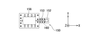
- the metal pattern layer 150 includes a probe 152 disposed on the protrusion 122 and a signal line pattern 153.
- the signal line pattern 153 includes a portion disposed in the cavity 121 a and a portion disposed in the protrusion 122.
- the probe 152 is connected to the semiconductor device 110 via the signal line pattern 153 and the bonding wire 199.
- the metal pattern layer 130 includes a ground pattern frame shape portion 131 disposed on the device mounting portion 121 and a ground pattern protrusion 132 disposed on the protrusion 122.
- the ground pattern protrusion 132 protrudes from the ground pattern frame shape portion 131 in the X direction.
- the ground pattern frame shape portion 131 surrounds the cavity 121a.
- the through hole 125 connects the ground pattern main part 171 and the ground pattern main part 191 to each other.
- the through hole 127 connects the ground pattern frame shape part 131, the ground pattern main part 171 and the ground pattern main part 191 to each other.
- the other through hole 127 connects the ground pattern protrusions 132, 172, and 192 to each other.
- the signal line pattern 153 is disposed between the ground pattern protrusions 132 and 172.
- the ground pattern protrusion 132, the signal line pattern 153, and the ground pattern protrusion 172 form a high-frequency transmission path 155.
- the high-frequency transmission line 155 has a stripline structure.
- the conductor cover 400 is attached to the surface of the printed board 200 so as to cover at least a part of the protrusion 122 and the opening 210.
- the metal case 300 is attached to the back surface of the printed board 200 so that the cavity of the waveguide 310 overlaps the opening 210 when viewed from the Z direction.
- FIG. 2 shows the internal structure in the vicinity of the protrusion 122 of the multilayer substrate 120.
- the multilayer substrate 120 includes dielectric layers 140, 160, and 180.
- the dielectric layers 140, 160, and 180 are represented as if they were transparent to show the internal structure.
- the dielectric layers 140, 160, and 180 are, for example, low temperature fired alumina ceramic substrates.
- the dielectric layer 180 is disposed between the metal pattern layer 190 and the metal pattern layer 170.
- the dielectric layer 160 is disposed between the metal pattern layer 170 and the metal pattern layer 150.
- the dielectric layer 140 is disposed between the metal pattern layer 150 and the metal pattern layer 130.
- the protrusion 122 of the multilayer substrate 120 protrudes from the device mounting portion 121 toward the opening 210 in the X direction.
- the tip of the protrusion 122 (the portion where the probe 152 is disposed) is disposed at a position overlapping the opening 210.
- the ground pattern protrusions 132, 172, and 192 are not disposed at positions that overlap the opening 210.
- the signal line pattern 153 is disposed between the ground pattern protrusions 132 and 172.
- the probe 152 is not disposed between the ground pattern protrusions 132 and 172 but is disposed at a position overlapping the opening 210.
- the signal line pattern 153 is parallel to the X direction.
- the signal line pattern 153 is sandwiched between the first through hole group and the second through hole group.
- the first through hole group includes a plurality of through holes 127 arranged in parallel to the X direction.
- the second through hole group includes a plurality of through holes 127 arranged in parallel with the X direction.
- the semiconductor package 100 according to the first embodiment can be connected to the waveguide 310 in a state where the semiconductor package 100 is mounted on the printed board 200 by surface mounting, and suppresses signal degradation due to the influence of higher-order modes. it can.
- the cavity 121a in which the semiconductor device 110 is disposed and the device mounting portion 121 in which the cavity 121a is formed have a rectangular shape.
- the width W2 of the protrusion 122 in the Y direction is smaller than the width W1 of the device mounting portion 121 in the Y direction.
- the metal pattern layer 150 includes an electrode pattern 156 disposed in the cavity 121a.
- the electrode pattern 156 is connected to the semiconductor device 110 via a bonding wire (not shown).
- the metal pattern layers 130, 150, 170, and 190 and the dielectric layers 140, 160, and 180 will be described with reference to FIGS. 4A to 4G.
- the metal pattern layer 130 includes a ground pattern frame shape portion 131 and a ground pattern projection portion 132 protruding from the ground pattern frame shape portion 131 in the X direction.
- the metal pattern layer 130 is formed on the dielectric layer 140 by firing, for example.
- the dielectric layer 140 includes a dielectric frame shape portion 141 surrounding the rectangular opening 140a and a dielectric protrusion 142 protruding from the dielectric frame shape portion 141 in the X direction.
- the metal pattern layer 150 includes a probe 152, a signal line pattern 153, and an electrode pattern 156.
- the metal pattern layer 150 is formed on the dielectric layer 160 by firing, for example.
- the dielectric layer 160 includes a dielectric frame shape portion 161 surrounding the rectangular opening 160a, and a dielectric protrusion 162 protruding from the dielectric frame shape portion 161 in the X direction.
- the opening 160a is smaller than the opening 140a.
- the metal pattern layer 170 includes a ground pattern main portion 171 and a ground pattern protrusion 172 protruding from the ground pattern main portion 171 in the X direction.
- the metal pattern layer 170 is formed on the dielectric layer 180 by firing, for example.
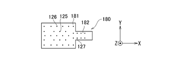
- the dielectric layer 180 includes a dielectric rectangular portion 181 and a dielectric protrusion 182 protruding from the dielectric rectangular portion 181 in the X direction.
- the metal pattern layer 190 includes a ground pattern main portion 191, a ground pattern protrusion 192 protruding from the ground pattern main portion 191 in the X direction, and an electrode pattern 196.
- the electrode pattern 196 is an electrode pattern for applying a DC bias to a circuit in the semiconductor device 110, for example.
- the electrode pattern 196 may be an electrode pattern for a low frequency signal (eg, LO signal or IF signal for an up-converter or down-converter).
- the metal pattern layer 190 is formed on the dielectric layer 180 by firing, for example.
- the ground pattern protrusion 132, the dielectric protrusion 142, the probe 152, another part of the signal line pattern 153, the dielectric protrusion 162, the ground pattern protrusion 172, the dielectric protrusion 182 and the ground pattern protrusion 192 are The multi-layer substrate 120 is disposed on the protrusion 122.
- the metal pattern layer 150 may be formed on the dielectric layer 140.
- the metal pattern layer 170 may be formed on the dielectric layer 160.
- the multilayer substrate 120 includes a through hole 126 in addition to the through holes 125 and 127 described above.
- the through hole 125 passes through the dielectric rectangular portion 181 and connects the ground pattern main portions 171 and 191 to each other.
- the through hole 126 penetrates the dielectric frame shape portion 161 and the dielectric rectangular portion 181 and connects the electrode patterns 156 and 196 to each other.
- the group of through holes 127 penetrates through the dielectric frame shape portion 141, the dielectric frame shape portion 161, and the dielectric rectangular portion 181 and passes through the ground pattern frame shape portion 131, the ground pattern main portion 171 and the ground pattern main portion. 191 are connected to each other.
- Another group of through holes 127 penetrate the dielectric protrusions 142, 162, and 182 and connect the ground pattern protrusions 132, 172, and 192 to each other.
- the through holes 125 to 127 are formed, for example, as hollow or solid conductors extending in the Z direction.
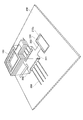
- metal patterns 201, 202, and 206 for mounting the semiconductor package 100 and a wiring pattern 208 are formed on the surface of the printed board 200.
- the metal pattern 201 is connected to the conductor wall 210 a of the opening 210 through the metal pattern 202.
- the metal patterns 201 and 202 form a ground plane.
- the metal pattern 206 forms an electrode pattern separated from the metal patterns 201 and 202.
- the wiring pattern 208 is connected to the metal pattern 206.
- the semiconductor device 110 and the CAP of the semiconductor package 100 are omitted.
- the metal patterns 201, 202, and 206 of the printed board 200, and the ground pattern main portion 191, the ground pattern protrusion 192, and the electrode pattern 196 of the semiconductor package 100 are mounted on the printed board 200 by the surface mounting technique. Used to do.
- the semiconductor package 100 is mounted on the printed board 200 by soldering.
- the ground pattern main portion 191 is disposed on the metal pattern 201
- the ground pattern protrusion 192 is disposed on the metal pattern 202
- the electrode pattern 196 is disposed on the metal pattern 206. Is placed.
- the lowermost metal pattern layer 190 of the semiconductor package 100 produces a self-alignment effect when the semiconductor package 100 is mounted on the printed board 200. Therefore, the accuracy of the mounting position of the semiconductor package 100 is improved.
- At least a part of the wiring pattern 208 is not disposed under the mounted semiconductor package 100.
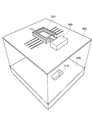
- the conductor cover 400 is attached to the surface of the printed board 200 so as to cover at least a part of the protrusion 212 of the semiconductor package 100 and the opening 210.
- the metal case 300 is attached to the back surface of the printed board 200 so that the waveguide 310 and the opening 210 overlap.
- FIG. 7 shows a result of simulating signal passing characteristics by three-dimensional electromagnetic field analysis for the protrusion 212 of the semiconductor package 100.
- the vertical axis in FIG. 7 indicates the signal pass characteristic
- the horizontal axis in FIG. 7 indicates the frequency of the signal.
- a simulation was performed for the case where the dielectric layers 140, 160, and 180 were formed of low-temperature fired alumina ceramic having a relative dielectric constant of 7.0.
- good signal passing characteristics were obtained in the 60 GHz band.
- the relative permittivity of the dielectric portion arranged in the waveguide is greatly different from 1, discontinuous points are formed in the signal transmission path, and the signal passing characteristic is deteriorated.
- the portion of the semiconductor package 100 protruding into the space above the waveguide 310 can be reduced. Therefore, it is possible to improve the pass characteristic of the high frequency signal.
- the semiconductor package 100 according to the first embodiment can be connected to the waveguide 310 while being mounted on the printed board 200 by surface mounting, and suppresses signal degradation due to the influence of higher-order modes. be able to.
- the mounting structure of the semiconductor package according to the first embodiment described above is a mounting structure of a semiconductor package having one port having a millimeter wave interface, but the mounting structure of the semiconductor package according to the second embodiment has a millimeter wave interface.
- This is a mounting structure of a semiconductor package having two ports.
- the protrusions 122 are provided on both sides of the device mounting portion 121.
- the number of metal pattern layers included in the multilayer substrate 120 is not limited to four. In addition to the four metal pattern layers 130, 150, 170, 190, other metal pattern layers may be added. If the high-frequency transmission line 155 has a microstrip line structure instead of a stripline structure, the number of metal pattern layers provided in the multilayer substrate 120 can be three.
- the cavity 121a in which the semiconductor device 110 is disposed is not limited to a two-stage structure, and may have a structure of three or more stages.
- the multilayer substrate 120 is not limited to a ceramic substrate.
- the dielectric layers 140, 160, 180 may be formed of an organic material instead of a ceramic material. Instead of the printed board 200, a board other than the printed board may be used.
- SYMBOLS 100 Semiconductor package 110 ... Semiconductor device 120 ... Multilayer substrate 121 ... Device mounting part 121a ... Cavity 122 ... Protrusion part 130, 150, 170, 190 ... Metal pattern layer 132 ... Ground pattern protrusion part 152 ... Probe 153 ... Signal line pattern 155 High-frequency transmission path 156 Electrode pattern 171 Ground pattern main part 172 Ground pattern protrusion 196 Electrode pattern 200 Print board 210 Opening 300 Metal case 310 Waveguide 400 Conductor cover W1, W2 Width
Landscapes
- Production Of Multi-Layered Print Wiring Board (AREA)
- Physics & Mathematics (AREA)
- Geometry (AREA)
- Structure Of Printed Boards (AREA)
Abstract
Description
以下、図面を参照して本発明の実施の形態について説明する。
図1は、実施の形態1にかかる半導体パッケージの実装構造の部分断面図を示す。実施の形態1にかかる半導体パッケージの実装構造は、ミリ波信号のような高周波信号を扱うのに適している。実施の形態1にかかる半導体パッケージの実装構造は、例えば、ミリ波発信器、ミリ波アップコンバータ、又はミリ波ダウンコンバータである。
図1を参照して、多層基板120は、セラミック多層基板として形成されている。多層基板の積層方向はZ方向に一致する。多層基板120は、半導体デバイス110が搭載されるデバイス搭載部121と、デバイス搭載部110から開口210に向かってX方向に突き出した突起部122とを備える。キャビティ121aは、デバイス搭載部121に形成される。キャビティ121aは、2段構造である。
上述した実施の形態1に係る半導体パッケージの実装構造は、ミリ波のインターフェイスを1ポート有する半導体パッケージの実装構造であるが、実施の形態2に係る半導体パッケージの実装構造は、ミリ波のインターフェイスを2ポート有する半導体パッケージの実装構造である。実施の形態2では、デバイス搭載部121の両側に突起部122が設けられる。
110…半導体デバイス
120…多層基板
121…デバイス搭載部
121a…キャビティ
122…突起部
130、150、170、190…メタルパターン層
132…グランドパターン突起部
152…プローブ
153…信号ラインパターン
155…高周波伝送路
156…電極パターン
171…グランドパターン主要部
172…グランドパターン突起部
196…電極パターン
200…プリント板
210…開口
300…金属ケース
310…導波管
400…導体カバー
W1、W2…幅
Claims (5)
- 導波管の空洞に接続される開口が形成された基板と、
前記基板に搭載された半導体パッケージと
を具備し、
前記半導体パッケージは、
半導体デバイスと、
前記半導体デバイスに接続されたプローブと
を備え、
前記開口は、
前記プローブと重なる部分と、
前記半導体パッケージと重ならない部分と
を備える
半導体パッケージの実装構造。 - 請求項1に記載の半導体パッケージの実装構造であって、
前記半導体パッケージは、多層基板を備え、
前記多層基板は、
前記半導体デバイスが搭載されるデバイス搭載部と、
前記デバイス搭載部から前記開口に向かって突き出した突起部と
を備え、
前記プローブは前記突起部に配置され、
前記突起部の幅は前記デバイス搭載部の幅より狭い
半導体パッケージの実装構造。 - 請求項2に記載の半導体パッケージの実装構造であって、
導波管短絡用の導体カバーと、
前記導波管が形成された金属ケースと
を更に具備し、
前記基板は、前記半導体パッケージが搭載される表面と、前記表面の反対側の裏面とを備え、
前記導体カバーは、前記突起部の少なくとも一部と前記開口とを覆うように前記表面に取り付けられ、
前記金属ケースは、前記導波管の前記空洞が前記開口と重なるように前記裏面に取り付けられ、
前記半導体デバイスは、前記デバイス搭載部に形成されたキャビティに配置され、
前記多層基板は、第1乃至第4メタルパターン層を備え、
前記第4メタルパターン層は、表面実装技術により前記半導体パッケージを前記基板に搭載するための第4層電極パターンを含み、
前記第3メタルパターン層は、前記第4メタルパターン層に比べて前記基板から遠く、
前記第2メタルパターン層は、前記第3メタルパターン層に比べて前記基板から遠く、
前記第1メタルパターン層は、前記第2メタルパターン層に比べて前記基板から遠く、
前記第1メタルパターン層は、前記突起部に配置された第1層グランドパターンを備え、
前記第2メタルパターン層は、前記半導体デバイスに接続される第2層電極パターンと、前記プローブと、ラインパターンとを備え、
前記第2層電極パターンは、前記キャビティ内に配置され、
前記プローブは、前記ラインパターンを介して前記半導体デバイスに接続され、
前記ラインパターンは、前記キャビティ内に配置された部分と、前記突起部内に配置された部分とを備え、
前記第3メタルパターン層は、前記キャビティの底に配置された第3層第1グランドパターンと、前記突起部に配置された第3層第2グランドパターンとを備え、
前記第3層第1グランドパターンの上に前記半導体デバイスが搭載され、
前記第1層グランドパターン、前記ラインパターン、及び前記第3層第2グランドパターンは、ストリップライン構造を形成する
半導体パッケージの実装構造。 - 半導体デバイスと、
多層基板と
を具備し、
前記多層基板は、
前記半導体デバイスが搭載されるデバイス搭載部と、
前記デバイス搭載部から突き出した突起部と、
前記突起部に配置されたプローブと
を備え、
前記プローブは、高周波伝送路を介して前記半導体デバイスに接続され、
前記突起部の幅は前記デバイス搭載部の幅より狭い
半導体パッケージ。 - プローブと、
前記プローブを介して導波路から高周波信号を入力又は当該導波路へ高周波信号を出力する半導体デバイスと
を具備し、
前記プローブは、前記導波路を構成する中空管内に突出し、かつ
前記中空管内に突出したプローブを含む面によって当該中空管を第1の空間と第2の空間に区画した場合に、当該第1の空間と当該第2の空間が連結されるように、前記プローブを覆う誘電体を構成した
半導体パッケージ。
Priority Applications (2)
| Application Number | Priority Date | Filing Date | Title |
|---|---|---|---|
| US14/438,734 US9577310B2 (en) | 2012-11-02 | 2013-06-25 | Semiconductor package and semiconductor package mounting structure |
| EP13850263.8A EP2916384B1 (en) | 2012-11-02 | 2013-06-25 | Semiconductor package and mounting structure thereof |
Applications Claiming Priority (2)
| Application Number | Priority Date | Filing Date | Title |
|---|---|---|---|
| JP2012-242580 | 2012-11-02 | ||
| JP2012242580 | 2012-11-02 |
Publications (1)
| Publication Number | Publication Date |
|---|---|
| WO2014068811A1 true WO2014068811A1 (ja) | 2014-05-08 |
Family
ID=50626769
Family Applications (1)
| Application Number | Title | Priority Date | Filing Date |
|---|---|---|---|
| PCT/JP2013/003956 Ceased WO2014068811A1 (ja) | 2012-11-02 | 2013-06-25 | 半導体パッケージ及びその実装構造 |
Country Status (3)
| Country | Link |
|---|---|
| US (1) | US9577310B2 (ja) |
| EP (1) | EP2916384B1 (ja) |
| WO (1) | WO2014068811A1 (ja) |
Cited By (3)
| Publication number | Priority date | Publication date | Assignee | Title |
|---|---|---|---|---|
| WO2015107588A1 (ja) * | 2014-01-16 | 2015-07-23 | 日本電気株式会社 | 半導体パッケージ、半導体装置及び送受信機 |
| CN105680133A (zh) * | 2016-01-11 | 2016-06-15 | 中国电子科技集团公司第十研究所 | 基片集成脊波导板间垂直互联电路结构 |
| US20240021553A1 (en) * | 2022-07-12 | 2024-01-18 | SK Hynix Inc. | Semiconductor device including two or more stacked semiconductor structures |
Families Citing this family (6)
| Publication number | Priority date | Publication date | Assignee | Title |
|---|---|---|---|---|
| US10325850B1 (en) * | 2016-10-20 | 2019-06-18 | Macom Technology Solutions Holdings, Inc. | Ground pattern for solderability and radio-frequency properties in millimeter-wave packages |
| US10818617B2 (en) * | 2018-09-28 | 2020-10-27 | Macom Technology Solutions Holdings, Inc. | Flange mount millimeter-wave package |
| JP7635784B2 (ja) * | 2020-08-07 | 2025-02-26 | 住友電気工業株式会社 | 高周波回路および無線装置 |
| SE544398C2 (en) * | 2020-09-11 | 2022-05-10 | Saab Ab | A transition arrangement |
| KR102864054B1 (ko) * | 2020-10-23 | 2025-09-24 | 삼성전자주식회사 | 인터포저를 포함하는 안테나 구조 및 이를 포함하는 전자 장치. |
| CN115207588A (zh) * | 2021-04-09 | 2022-10-18 | 华为技术有限公司 | 一种转接装置、电子设备、终端和转接装置的制备方法 |
Citations (7)
| Publication number | Priority date | Publication date | Assignee | Title |
|---|---|---|---|---|
| JPH06132708A (ja) * | 1992-09-30 | 1994-05-13 | Nec Corp | マイクロ波icモジュール |
| JPH11243307A (ja) | 1997-11-26 | 1999-09-07 | Trw Inc | ミリメートル波ltccパッケージ |
| JPH11340414A (ja) | 1998-05-28 | 1999-12-10 | Nec Corp | マイクロ波集積回路マルチチップモジュール、マイクロ波集積回路マルチチップモジュールの実装構造 |
| JP2003309404A (ja) * | 2002-04-17 | 2003-10-31 | Sharp Corp | 多層基板および衛星放送受信装置 |
| US20080111654A1 (en) * | 2004-11-30 | 2008-05-15 | Patrik Rivas | Transmission Arrangement |
| JP2008524887A (ja) * | 2004-12-20 | 2008-07-10 | ユナイテッド モノリシック セミコンダクターズ エスアーエス | マイクロ波用途のための小型電子部品 |
| JP2010098609A (ja) * | 2008-10-17 | 2010-04-30 | Nec Corp | 導波管−マイクロストリップ線路変換器、及び、その製造方法 |
Family Cites Families (11)
| Publication number | Priority date | Publication date | Assignee | Title |
|---|---|---|---|---|
| US3579149A (en) * | 1969-12-08 | 1971-05-18 | Westinghouse Electric Corp | Waveguide to stripline transition means |
| US4716386A (en) | 1986-06-10 | 1987-12-29 | Canadian Marconi Company | Waveguide to stripline transition |
| JPH1065038A (ja) * | 1996-08-22 | 1998-03-06 | Mitsubishi Electric Corp | ミリ波デバイス用パッケージ |
| SE514426C2 (sv) * | 1999-06-17 | 2001-02-19 | Ericsson Telefon Ab L M | Anordning för chipmontering i kavitet i flerlagers mönsterkort |
| JP4261726B2 (ja) | 2000-03-15 | 2009-04-30 | 京セラ株式会社 | 配線基板、並びに配線基板と導波管との接続構造 |
| EP1506595A4 (en) | 2002-04-19 | 2005-07-27 | Roadeye Flr General Partnershi | RF SYSTEM CONCEPT FOR A VEHICLE RADAR WITH MULTIPLE RADIATIONS |
| US7276988B2 (en) * | 2004-06-30 | 2007-10-02 | Endwave Corporation | Multi-substrate microstrip to waveguide transition |
| DE102006023123B4 (de) * | 2005-06-01 | 2011-01-13 | Infineon Technologies Ag | Abstandserfassungsradar für Fahrzeuge mit einem Halbleitermodul mit Komponenten für Höchstfrequenztechnik in Kunststoffgehäuse und Verfahren zur Herstellung eines Halbleitermoduls mit Komponenten für ein Abstandserfassungsradar für Fahrzeuge in einem Kunststoffgehäuse |
| US8912858B2 (en) * | 2009-09-08 | 2014-12-16 | Siklu Communication ltd. | Interfacing between an integrated circuit and a waveguide through a cavity located in a soft laminate |
| US8592960B2 (en) * | 2010-08-31 | 2013-11-26 | Viasat, Inc. | Leadframe package with integrated partial waveguide interface |
| US8912634B2 (en) * | 2012-03-29 | 2014-12-16 | International Business Machines Corporation | High frequency transition matching in an electronic package for millimeter wave semiconductor dies |
-
2013
- 2013-06-25 US US14/438,734 patent/US9577310B2/en not_active Expired - Fee Related
- 2013-06-25 EP EP13850263.8A patent/EP2916384B1/en not_active Not-in-force
- 2013-06-25 WO PCT/JP2013/003956 patent/WO2014068811A1/ja not_active Ceased
Patent Citations (7)
| Publication number | Priority date | Publication date | Assignee | Title |
|---|---|---|---|---|
| JPH06132708A (ja) * | 1992-09-30 | 1994-05-13 | Nec Corp | マイクロ波icモジュール |
| JPH11243307A (ja) | 1997-11-26 | 1999-09-07 | Trw Inc | ミリメートル波ltccパッケージ |
| JPH11340414A (ja) | 1998-05-28 | 1999-12-10 | Nec Corp | マイクロ波集積回路マルチチップモジュール、マイクロ波集積回路マルチチップモジュールの実装構造 |
| JP2003309404A (ja) * | 2002-04-17 | 2003-10-31 | Sharp Corp | 多層基板および衛星放送受信装置 |
| US20080111654A1 (en) * | 2004-11-30 | 2008-05-15 | Patrik Rivas | Transmission Arrangement |
| JP2008524887A (ja) * | 2004-12-20 | 2008-07-10 | ユナイテッド モノリシック セミコンダクターズ エスアーエス | マイクロ波用途のための小型電子部品 |
| JP2010098609A (ja) * | 2008-10-17 | 2010-04-30 | Nec Corp | 導波管−マイクロストリップ線路変換器、及び、その製造方法 |
Non-Patent Citations (1)
| Title |
|---|
| See also references of EP2916384A4 |
Cited By (4)
| Publication number | Priority date | Publication date | Assignee | Title |
|---|---|---|---|---|
| WO2015107588A1 (ja) * | 2014-01-16 | 2015-07-23 | 日本電気株式会社 | 半導体パッケージ、半導体装置及び送受信機 |
| CN105680133A (zh) * | 2016-01-11 | 2016-06-15 | 中国电子科技集团公司第十研究所 | 基片集成脊波导板间垂直互联电路结构 |
| US20240021553A1 (en) * | 2022-07-12 | 2024-01-18 | SK Hynix Inc. | Semiconductor device including two or more stacked semiconductor structures |
| US12354984B2 (en) * | 2022-07-12 | 2025-07-08 | SK Hynix Inc. | Semiconductor device including two or more stacked semiconductor structures |
Also Published As
| Publication number | Publication date |
|---|---|
| EP2916384A1 (en) | 2015-09-09 |
| EP2916384A4 (en) | 2016-06-22 |
| EP2916384B1 (en) | 2019-05-08 |
| US20150311576A1 (en) | 2015-10-29 |
| US9577310B2 (en) | 2017-02-21 |
Similar Documents
| Publication | Publication Date | Title |
|---|---|---|
| WO2014068811A1 (ja) | 半導体パッケージ及びその実装構造 | |
| JP7264884B2 (ja) | フェーズドアレイアンテナ | |
| EP3780259B1 (en) | Transition structure and multilayer transition structure for millimeter wave | |
| US9433080B2 (en) | High-frequency circuit package and sensor module | |
| EP2575167B1 (en) | Electronic device | |
| EP2945222A1 (en) | A microwave or millimeter wave RF part using pin grid array (PGA) and/or ball grid array (BGA) technologies | |
| CN102593565B (zh) | 电介质波导管的输入输出连接构造 | |
| US20180177041A1 (en) | Surface Integrated Waveguides and Circuit Structures Therefor | |
| KR101887356B1 (ko) | 도파관-전송선로 천이장치 | |
| JP5616927B2 (ja) | ホーンアンテナ一体型mmicパッケージ及びアレーアンテナ | |
| JP4081284B2 (ja) | 高周波集積回路モジュール | |
| CN105230136B (zh) | 电路基板、电子部件收纳用封装件以及电子装置 | |
| US20100001808A1 (en) | Planar transmission line-to-waveguide transition apparatus and wireless communication module having the same | |
| WO2012081288A1 (ja) | 高周波用パッケージ | |
| JP3347607B2 (ja) | 積層型導波管線路 | |
| CN104254945B (zh) | 连接高频电路和波导管的连接结构及其制造方法 | |
| US20240380089A1 (en) | Waveguide | |
| WO2022071256A1 (ja) | 配線基体および電子装置 | |
| CN118451604A (zh) | 用于雷达传感器的高频组件 | |
| JP2011010242A (ja) | 高周波基板および高周波モジュール | |
| JP2003133471A (ja) | 高周波信号用の配線基板 | |
| JP2003124636A (ja) | 配線基板 | |
| JP2005175874A (ja) | 伝送線路及び高周波モジュール |
Legal Events
| Date | Code | Title | Description |
|---|---|---|---|
| 121 | Ep: the epo has been informed by wipo that ep was designated in this application |
Ref document number: 13850263 Country of ref document: EP Kind code of ref document: A1 |
|
| WWE | Wipo information: entry into national phase |
Ref document number: 14438734 Country of ref document: US |
|
| NENP | Non-entry into the national phase |
Ref country code: DE |
|
| WWE | Wipo information: entry into national phase |
Ref document number: IDP00201502726 Country of ref document: ID |
|
| WWE | Wipo information: entry into national phase |
Ref document number: 2013850263 Country of ref document: EP |
|
| NENP | Non-entry into the national phase |
Ref country code: JP |