WO2014077163A1 - 磁気センサ装置 - Google Patents
磁気センサ装置 Download PDFInfo
- Publication number
- WO2014077163A1 WO2014077163A1 PCT/JP2013/080021 JP2013080021W WO2014077163A1 WO 2014077163 A1 WO2014077163 A1 WO 2014077163A1 JP 2013080021 W JP2013080021 W JP 2013080021W WO 2014077163 A1 WO2014077163 A1 WO 2014077163A1
- Authority
- WO
- WIPO (PCT)
- Prior art keywords
- output
- magnetic
- value
- transport time
- magnetic detection
- Prior art date
- Legal status (The legal status is an assumption and is not a legal conclusion. Google has not performed a legal analysis and makes no representation as to the accuracy of the status listed.)
- Ceased
Links
Images





Classifications
-
- G—PHYSICS
- G06—COMPUTING OR CALCULATING; COUNTING
- G06K—GRAPHICAL DATA READING; PRESENTATION OF DATA; RECORD CARRIERS; HANDLING RECORD CARRIERS
- G06K7/00—Methods or arrangements for sensing record carriers, e.g. for reading patterns
- G06K7/08—Methods or arrangements for sensing record carriers, e.g. for reading patterns by means detecting the change of an electrostatic or magnetic field, e.g. by detecting change of capacitance between electrodes
- G06K7/082—Methods or arrangements for sensing record carriers, e.g. for reading patterns by means detecting the change of an electrostatic or magnetic field, e.g. by detecting change of capacitance between electrodes using inductive or magnetic sensors
- G06K7/087—Methods or arrangements for sensing record carriers, e.g. for reading patterns by means detecting the change of an electrostatic or magnetic field, e.g. by detecting change of capacitance between electrodes using inductive or magnetic sensors flux-sensitive, e.g. magnetic, detectors
- G06K7/088—Methods or arrangements for sensing record carriers, e.g. for reading patterns by means detecting the change of an electrostatic or magnetic field, e.g. by detecting change of capacitance between electrodes using inductive or magnetic sensors flux-sensitive, e.g. magnetic, detectors using magneto-sensitive switches, e.g. reed-switches
-
- G—PHYSICS
- G01—MEASURING; TESTING
- G01R—MEASURING ELECTRIC VARIABLES; MEASURING MAGNETIC VARIABLES
- G01R33/00—Arrangements or instruments for measuring magnetic variables
- G01R33/0094—Sensor arrays
-
- G—PHYSICS
- G01—MEASURING; TESTING
- G01R—MEASURING ELECTRIC VARIABLES; MEASURING MAGNETIC VARIABLES
- G01R33/00—Arrangements or instruments for measuring magnetic variables
- G01R33/02—Measuring direction or magnitude of magnetic fields or magnetic flux
- G01R33/10—Plotting field distribution ; Measuring field distribution
-
- G—PHYSICS
- G06—COMPUTING OR CALCULATING; COUNTING
- G06K—GRAPHICAL DATA READING; PRESENTATION OF DATA; RECORD CARRIERS; HANDLING RECORD CARRIERS
- G06K7/00—Methods or arrangements for sensing record carriers, e.g. for reading patterns
- G06K7/08—Methods or arrangements for sensing record carriers, e.g. for reading patterns by means detecting the change of an electrostatic or magnetic field, e.g. by detecting change of capacitance between electrodes
- G06K7/082—Methods or arrangements for sensing record carriers, e.g. for reading patterns by means detecting the change of an electrostatic or magnetic field, e.g. by detecting change of capacitance between electrodes using inductive or magnetic sensors
- G06K7/087—Methods or arrangements for sensing record carriers, e.g. for reading patterns by means detecting the change of an electrostatic or magnetic field, e.g. by detecting change of capacitance between electrodes using inductive or magnetic sensors flux-sensitive, e.g. magnetic, detectors
Definitions
- the present invention relates to a magnetic sensor device that detects a magnetic pattern of a medium such as a magnetic ink print, a magnetic recording medium, or a magnetic slit scale.
- a magnetic sensor device is used to convert a pattern printed with magnetic ink, which is used for a medium requiring high security, such as banknotes and checks, into electrical information, and determine the authenticity of the medium based on the information.
- a medium requiring high security such as banknotes and checks
- a magnetic sensor device used for a banknote recirculation-type ATM automated deposit / payment / payment machine
- a banknote counter for business use or a banknote sorter that requires advanced banknote discrimination many magnetic detection elements covering the entire width of a banknote or check Is placed in the banknote processing unit so that more magnetic information can be used for discrimination or discrimination.
- Patent Document 1 a magnetoresistive sensor arranged in the middle of a moving path of a magnetic material, a lower magnet in which S and N poles are arranged along the moving direction of the magnetic material, and along the moving direction of the magnetic material.
- a magnetic body detection device including an upper magnet in which N and S poles are arranged is described.
- the south pole of the lower magnet and the north pole of the upper magnet are opposed to each other, and the north pole of the lower magnet and the south pole of the upper magnet are opposed to each other via the magnetic path.
- a plurality of magnetoresistive sensors are arranged linearly. Output signals from the respective magnetoresistive sensors are supplied to the processing circuit simultaneously or in time series, and are stored in the processing circuit as one-dimensional image signals. A two-dimensional magnetic pattern image can be acquired by performing such a reading operation each time the magnetic body moves at a predetermined pitch.
- Patent Document 1 describes that signal processing is performed by converting output signals of a plurality of magnetoresistive sensors into digital values by an AD converter. In that case, in order to sample the output signal, it becomes discrete information with respect to time.
- the magnetic sensor device performs individual readout by a readout circuit composed of an analog circuit for each magnetic detection element. Therefore, a continuous magnetic signal output can be obtained in the transport direction.
- the interval between the magnetic detection elements is about 10 mm in the reading width direction, and the resolution in the width direction is not high compared to the magnetic pattern printed on the medium.
- the present invention has been made to solve the above-described problems, and aims to simplify the read circuit for the output signals of a plurality of magnetic detection elements and increase the reading resolution of the magnetic pattern. .
- the magnetic sensor device includes a magnetic detection element and a bias magnet for applying a bias magnetic field to the magnetic detection element with a magnetic force line in a fixed direction.
- the magnetic sensor device detects a magnetic field variation when a medium having a magnetic pattern passes a bias magnetic field as an electric signal by a magnetic detection element, and reads the magnetic pattern of the medium.
- a plurality of magnetic detection elements are arranged along a reading line that intersects in the direction of relative movement with the medium.
- a plurality of switches are connected to each of the magnetic detection elements and an output line common to the plurality of magnetic detection elements. Then, the switch control unit sequentially closes the switches one by one and takes out the outputs of the magnetic detection elements one by one to the common output line.
- the magnetic sensor device of the present invention since the outputs of the plurality of magnetic detection elements arranged along the reading line are sequentially taken out to the common output line, the output signal readout circuit of the plurality of magnetic detection elements is simplified. As a result, the reading resolution of the magnetic pattern can be increased.
- FIG. 1 is a conceptual diagram of a magnetic sensor device according to an embodiment of the present invention. It is a conceptual diagram of the medium conveyance in a magnetic sensor apparatus.
- 1 is a block diagram illustrating a configuration example of a magnetic sensor device according to a first embodiment.
- 3 is a block diagram illustrating a configuration example of a correction circuit according to the first embodiment.
- FIG. It is a schematic diagram which shows the output of a magnetic detection element. It is a schematic diagram which shows the output of the magnetic detection element after offset adjustment. It is a figure which shows the example of the output of a magnetic detection element.
- FIG. 7B is an enlarged view of a portion surrounded by a dotted ellipse in FIG. 7A.
- FIG. 3 is a diagram showing a magnetic pattern reading sequence according to the first embodiment. It is a block diagram which shows the structural example of the correction circuit which concerns on Embodiment 2 of this invention. It is a figure which shows the example of the dead zone which concerns on Embodiment 2. FIG. It is a figure which shows the example of the output selection of the magnetic detection element which concerns on Embodiment 2. FIG. It is a schematic diagram which shows the absolute value output of a magnetic detection element. It is a figure explaining the difference of the output timing for every magnetic detection element.
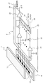
- FIG. 1 is a conceptual diagram of a magnetic sensor device according to an embodiment of the present invention.
- the magnetic sensor device according to the embodiment includes a magnetic detection module 1 and a signal readout circuit 2.
- the magnetic detection module 1 includes a substrate 12 on which a plurality of magnetic detection elements 11 are mounted, and a magnet 13.
- the plurality of magnetic detection elements 11 are arranged along a reading line that intersects the transport direction (relative movement direction) of a medium having a magnetic pattern.
- the magnetic detection element 11 is, for example, a semiconductor magnetoresistive (SMR) element.
- SMR semiconductor magnetoresistive
- the magnetic detection element 11 is linearly arranged on the substrate 12 over a width of 200 mm at a constant interval of 0.5 mm, for example. In that case, the number of the magnetic detection elements 11 is 400.
- the substrate 12 is disposed between the two magnets 13.
- the magnet 13 is arranged so that the lines of magnetic force are applied in a certain direction with respect to the magnetic detection element 11, and a magnetic field having a constant intensity is constantly applied to the magnetic detection element 11. Since the direction in which the semiconductor magnetoresistive element feels the magnetic field is a direction perpendicular to the detection surface of the element, in that case, a bias magnetic field is applied in a direction perpendicular to the detection surface of the element.
- the two magnets 13 form a substantially uniform magnetic field in the arrangement direction of the plurality of magnetic detection elements 11.
- a signal reading circuit 2 including a semiconductor circuit for reading the output of the magnetic detection element 11 on the substrate 12 is connected to the substrate 12.
- the substrate 12 and the signal readout circuit 2 are connected to the electrode of the substrate 12 by, for example, Au wire or Al wire. Further, a power supply line of a reference bias voltage and a bias electrode of the substrate 12 are connected.
- the output of the magnetic detection element 11 is connected to the readout switch 22 via the individual readout circuit 21 such as a gate and an amplifier.
- Each magnetic detection element 11 outputs a signal that swings positive and negative with a predetermined offset voltage as a reference. Detecting offset voltage variations and temperature fluctuations of the individual magnetic detection elements 11 in a blanking period in which the magnetic pattern is not at the position of the reading line, for example, a period in which no medium such as banknotes is present in the magnetic detection module 1, The variation and temperature fluctuation amount are stored.
- the individual reading circuit 21 corrects each offset voltage variation and temperature variation and performs predetermined amplification.
- the read switch 22 is provided for each magnetic detection element 11 and is connected to the magnetic detection element 11 via the individual read circuit 21.
- the other end of the read switch 22 is connected to an output line 28 via a common amplifier circuit 26 common to the plurality of magnetic detection elements 11.
- Each of the read switches 22 is controlled to be turned on / off according to the state of the corresponding bit of the shift register 23. From the data line 24, only the bit of the shift register 23 corresponding to the one end read switch 22 sets data for turning on the read switch 22, and the other bits set data for turning off the switch.
- a clock is applied from the clock line 25 to the shift register 23, the data is shifted to the adjacent bit in one direction.
- bit shifting for example, data overflowing from the last bit is input to the first bit (that is, the data circulates through the shift register 23).
- Each time a clock is applied data is shifted to the adjacent bit, so that the read switch 22 can be turned on one by one from the end.
- the common amplifier circuit 26 only the output of one magnetic detection element 11 in which the corresponding readout switch 22 is turned on is input to the common amplifier circuit 26.
- the operation of taking out the outputs of all the magnetic detection elements 11 of the plurality of magnetic detection elements 11 to the common output line 28 once is defined as a read cycle.
- the control signal 27 is turned on to connect the output of the magnetic detection element 11 to the individual read circuit 21.
- the read cycle can be executed by causing the shift register 23 to make a round of data for which the read switch 22 is turned on.
- the shift register 23 is an example of a switch control unit. The execution of the read cycle is not limited to the method using the shift register 23 described above.
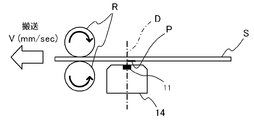
- FIG. 2 is a conceptual diagram of medium conveyance in the magnetic sensor device.
- the substrate 12 and the lower magnet 13 are collectively shown as a magnetic sensor unit 14.
- a medium S from which magnetic information is to be read is transported by a transport roller R, and the medium S passes through a reading line D of the magnetic detection element 11 at a transport speed V (mm / sec).
- the medium S from which magnetic information is read by the magnetic sensor device 10 is, for example, a bill, a check, other securities, or the like having a magnetic pattern P on which a predetermined pattern is printed with magnetic ink.
- the medium S is transported between the magnet 13 and the substrate 12 in FIG. 1 in a direction intersecting with the arrangement direction of the magnetic detection elements 11, for example, a direction orthogonal to the arrangement direction.
- the output of the magnetic detection element 11 corresponding to the magnetic pattern P arriving at the read line D is 1 over a plurality of magnetic detection elements 11 for each read cycle. One by one is taken out to the output line 28 in sequence.
- the extraction of the outputs of the plurality of magnetic detection elements 11 along the reading line D is called main scanning.
- repeating the read cycle by transporting (relatively moving) the medium S is called sub-scanning.
- the output of the main scanning magnetic detection element 11 appears in time series on one output line 28, and the main scanning output repeatedly appears in time series on one output line 28 for each read cycle. In this way, two-dimensional information of the magnetic pattern P of the medium S is obtained as a time-series signal on one output line 28.
- FIG. 3 is a block diagram illustrating a configuration example of the magnetic sensor device according to the first embodiment.
- the magnetic information signal output from the signal readout circuit 2 to the signal line common to the magnetic detection element 11 is transferred to the common signal processing unit 3.
- the signal is amplified again by the offset amplification circuit 4 and an offset voltage is added so as to obtain an optimum signal dynamic range for subsequent processing.
- ADC analog-digital converter
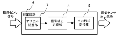
- FIG. 4 is a block diagram illustrating a configuration example of the correction circuit according to the first embodiment.
- the correction circuit 6 includes an offset adjustment unit 7, a signal correction processing unit 8, and an output format conversion unit 9.
- the magnetic information signal digitized by the ADC 5 is a signal having an offset voltage added by the analog circuit group in the previous stage. As shown in FIG. It is not clear whether to take the value. Therefore, correction is performed based on a blank period signal without a magnetic pattern.
- an output value in a period without a magnetic signal is determined.
- the fluctuation from the output value in the blank period is regarded as a magnetic information signal, and a process is performed to adjust so that the midpoint of the dynamic range of the digital signal of the magnetic information signal is a uniform offset in all the magnetic detection elements 11. For example, as shown in FIG. 6, if the dynamic range of the digital output is 255 steps, the magnetic information signal is always based on the midpoint (128) of the digital output value. Since the reference of the signals of the plurality of magnetic detection elements 11 is aligned, subsequent signal processing and discrimination become easy.
- the magnetic information signal processed in this way is further transferred to the signal processing unit 3 at the subsequent stage.
- the signal correction processing unit 8 performs reading on a reference magnetic medium in advance, and corrects the magnetic detection sensitivity with individual variations using the correction circuit 6 in which the output of each magnetic detection element 11 is stored. When the reference magnetic medium is read, the output is made constant at each magnetic detection element 11. This correction processing can be turned on / off as necessary.
- the output format conversion unit 9 adds a signal indicating the data output period of the magnetic information, the synchronization clock, and the detection line delimiter to the magnetic information signal output from the signal correction processing unit 8, and serves as the output of the magnetic sensor.
- FIG. 7A is a diagram showing an example of the output of the magnetic detection element.
- FIG. 7A shows the output of the magnetic detection element 11 including a portion without magnetic information.
- FIG. 7B is an enlarged view of a portion surrounded by a dotted ellipse in FIG. 7A.
- the output of one magnetic detection element 11 changes with time as shown in FIG. 7A as the medium is conveyed as shown in FIG.
- the magnetic pattern on a certain line along the sub-scanning direction of the medium can be read. If the medium is transported at a constant speed, the magnetic pattern on the sub-scanning line can be read at regular intervals by performing reading at a constant cycle.
- the outputs of the plurality of magnetic detection elements 11 appear serially on the common output line 28 by the switch of the signal readout circuit 2, but the data on the common output line 28 is sampled in synchronization with the clock applied to the shift register 23.
- the outputs of the plurality of magnetic detection elements 11 can be read as time-series serial data. If sampling data is taken in accordance with a cycle (read cycle) in which the data of the shift register 23 makes a round, the output of one magnetic detection element 11 can be obtained.
- the reading time per line (one reading cycle) is 0.25 msec. It is.
- FIG. 8A is a diagram illustrating an example of sampling of the output of the magnetic detection element.
- FIG. 8A shows the range of FIG. 7B.
- FIG. 8B is an enlarged view of a portion surrounded by a dotted ellipse in FIG. 8A.
- FIG. 8A shows the output of one magnetic detection element 11.
- the output of one magnetic sensing element 11 appears on the common output line 28 for the time that the switch is turned on during the read cycle. For the remaining time, the outputs of the other magnetic detection elements 11 appear in order on the common output line 28.
- Sampling of the output of the magnetic detection element 11 is performed at the position of the magnetic detection element 11 in the section of the read cycle (time when the switch is turned on).
- the value of the sampling timing is set as an output value (magnetic sensor output) of the reading cycle of the magnetic detection element 11.
- FIG. 9 is a diagram showing a magnetic pattern reading sequence according to the first embodiment. The entire magnetic pattern information of the medium to be read is read as shown in FIG. 9, whereby information from the plurality of magnetic detection elements 11 is obtained as two-dimensional image information.
- the magnetic sensor device 10 is configured to perform sampling in the main scanning direction (reading cycle) of the magnetic detection element 11 and repetition of the main scanning (reading cycle) in the sub-scanning direction in synchronization with the conveyance of the medium. Therefore, it is easy to take compatibility between the line image sensor for reading optical information and the data format. As a result, magnetic information and optical information can be processed in the same manner.
- FIG. 10 is a block diagram showing a configuration example of a correction circuit according to Embodiment 2 of the present invention.
- the correction circuit 6 according to the second embodiment includes an output selection unit 61 in addition to the configuration of the first embodiment.
- the output selection unit 61 stores the output value of the previous read cycle for each magnetic detection element 11.
- the same value as the output value of the previous read cycle is set as the output value of the read cycle. In that case, the stored output of the previous read cycle is not updated.
- the output of the read cycle is set as the output value, and the output value of the previous read cycle stored is set as the output value of the read cycle. replace.
- FIG. 11 is a diagram illustrating an example of a dead range according to the second embodiment.
- the actual output from each magnetic detection element 11 includes a noise component.
- a predetermined insensitive range is determined from the output of the previous read cycle.
- the range of a predetermined value above and below is defined as the dead range with the output of the previous read cycle as the center.
- FIG. 12 is a diagram illustrating an example of output selection of the magnetic detection element according to the second embodiment.
- FIG. 12 is an enlarged view of a range surrounded by a dotted line in FIG. The dead zone is indicated by a horizontal dotted line.
- the value of the sampling timing is indicated by a black circle.
- the output of the magnetic sensor is the height of the solid line passing through the black circle.
- the output selection unit 61 is not limited to being before the offset adjustment unit 7, but may be before the signal correction processing unit 8 or before the output format conversion unit 9.
- the magnetic detection elements 11 are arranged at a pitch of 0.5 mm in a detection width of 200 mm and have 400 magnetic detection elements 11. Assuming that the pitch of the magnetic detection elements 11 is the same as the detection pitch in the conveyance direction by medium conveyance, and the detection period per read cycle is 0.25 msec, the medium conveyance speed is 2 m / sec, and extremely high-speed magnetic information detection is performed. Is possible. Further, the data output clock at this time is about 2 MHz, and can be easily connected to the banknote discrimination system.
- the effective reading width of the medium is 200 mm, but the effective reading width can be changed to an arbitrary size.
- the effective width of reading can be reduced to about 100 mm or less by using the short side of the banknote as the arrangement direction (main scanning direction) of the magnetic detection elements 11.
- ) is calculated from the reference point. It is also possible to adopt an output method. By performing such processing, it is possible to process an image with only the magnitude of the magnetic information without considering the directionality of the magnetic signal.
- Embodiment 3 In the third embodiment, a plurality of read cycles are performed while the medium is transported for the same length as the interval between adjacent magnetic detection elements 11 along the read line.
- the time when the relative movement distance of the medium is the same as the interval between the adjacent magnetic detection elements 11 along the reading line is referred to as a unit transport time.
- Embodiments 1 and 2 are cases in which one read cycle is performed per unit transport time.
- the resolution of the density of the magnetic detection elements 11 can be obtained in the arrangement direction of the magnetic detection elements 11, but the resolution in the medium transport direction depends on the density of the read cycle. Further, the output of each magnetic detection element 11 in one read cycle is limited to the time during which the read switch 22 in FIG. 1 is closed. For example, when the frequency of the clock applied to the shift register 23 is 2 MHz, the output time of one magnetic detection element 11 in one read cycle is 0.5 ⁇ sec. Assuming that the conveyance speed is 2 m / sec and the interval between the magnetic detection elements 11 is 0.5 mm, the unit conveyance time is 0.25 msec as described above. When the clock frequency is 2 MHz, the output time 0.5 ⁇ sec of the magnetic detection element 11 is extremely short compared to the unit transport time 0.25 msec.
- the resolution with respect to the transport direction can decompose only a repetitive pattern of about 2 kHz (resolution of about 1 mm) with respect to a read cycle frequency of 4 kHz (number of read cycles per second), and is a space larger than the read cycle frequency.
- a magnetic pattern having a frequency fluctuations in most of the period in the transport direction are missed.
- the reading position in one reading cycle is shifted by the amount of movement of the medium because the output from the first element to the last element has a difference in the selection time in the shift register 23.
- FIG. 15A is a diagram illustrating output positions of the line head element and the line end element.
- FIG. 15B is a diagram illustrating an error due to a difference in output timing.
- 15B shows the case of being output at the beginning of the read cycle by a black circle and the case of being output at the end of the read line by an asterisk.
- the magnetic pattern of the medium changes in the transport direction, it is shown that there is a difference in the transport distance during the read cycle time between the output at the head position and the output at the final position (FIG. 15B).
- a plurality of read cycles are performed during the unit conveyance time.
- the configuration of the magnetic sensor device 10 according to the third embodiment is the same as that of the first embodiment.
- the frequency of the clock applied to the shift register 23 is adjusted so that a plurality of read cycles are performed during the unit transport time.
- a plurality of sampling data is obtained for each magnetic detection element 11 in the unit conveyance time.
- FIG. 17 is a diagram showing a magnetic pattern reading sequence according to the third embodiment of the present invention.
- the basic operation is the same as in the first embodiment, but the read cycle is performed a plurality of times in one unit transport time (for example, 0.25 msec).
- reading of one unit conveyance time that is, sub-scanning in units of the same distance as the interval between the magnetic detection elements 11 is represented by “line”.
- one line one unit transport time
- one line includes M read cycles. For example, eight read cycles are performed per unit transport time using a clock having a frequency that is eight times the frequency of performing one read cycle per unit transport time.
- sampling is performed in synchronization with the clock applied to the shift register 23 in the read cycle, so that M pieces of data are obtained for each magnetic detection element 11 in one unit transport time. For example, when 8 read cycles are performed in the unit transport time, 8 pieces of sampling data are obtained.
- the signal correction processing unit 8 determines the output value of the unit transport time based on the output of a plurality of read cycles of the unit transport time. For example, an average value, a maximum value, a minimum value, or the like of a plurality of data for a unit transport time can be considered.
- a moving averaging process may be performed in order to remove noise components having a frequency higher than the frequency of the read cycle.
- the moving average process is performed by the offset adjustment unit 7 of the correction circuit 6 of FIG.
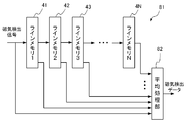
- FIG. 18 is a block diagram illustrating a configuration example of the moving average processing unit.
- the moving average processing unit 81 has the number of line memories 41, 42, 43,. . . 4N and an average processing unit 82 are provided.
- Each of the line memories 41 to 4N stores data of one read cycle instead of “line” data of one unit transport time.
- Data sampled by the ADC 5 is stored in the line memory 41 for each read cycle.
- the data stored in the line memory 41 is transferred to the next line memories 42 to 4N every read cycle.
- the average processing unit 82 obtains moving average data by averaging the data of the plurality of line memories 41 to 4N and the latest read cycle data for each magnetic detection element 11.
- FIG. 19A is a conceptual diagram showing output noise and moving average of the magnetic detection element.
- FIG. 19A shows the relationship between the output of the magnetic detection element 11 and the moving average output.
- FIG. 19B is an enlarged view of a portion surrounded by a dotted ellipse in FIG. 19A.
- the output of the magnetic detection element 11 fluctuates at a frequency higher than the frequency of the unit conveyance time, whereas the moving average output is smoothed by averaging high frequency components.
- the removal of the noise component of the output of the magnetic detection element 11 is not limited to the simple moving average.
- a value represented by the following formula can be used.
- the corrected moving average is obtained by multiplying the contribution ratio of data in the latest read cycle by 1 / (N + 1) times and sequentially reducing the contribution ratio to N / (N + 1).
- the constant N is set according to the spatial frequency characteristics of the magnetic pattern. For example, the basic spatial frequency component (in the sub scanning direction) of the magnetic pattern is set so as not to attenuate.
- the moving average processing unit 81 can use a weighted moving average, an exponential moving average (generalized corrected moving average), or the like.
- the signal correction processing unit 8 calculates output data of the unit transport time from M outputs of the unit transport time or M moving average outputs.
- FIG. 20 is a block diagram illustrating an example of an output calculation unit included in the signal correction processing unit 8.
- the line memories 41 to 4N are indicated by a line memory 40.
- the output calculation unit 83 includes M line memories 51, 52, 53,. . . 5M and an output value determination circuit 84 are provided.
- Each of the line memories 51 to 5M stores an output of one read cycle or an output of one read cycle subjected to moving average.
- the data in the line memory 51 of the output calculation unit 83 is transferred to the next line memories 52 to 5M every read cycle, like the line memory 41 of the moving average process.
- FIG. 21 is a diagram showing an output calculation when outputting an average value for each unit conveyance time.
- the output value determination circuit 84 of the output calculation unit 83 calculates, for example, an average of M outputs (eight in FIG. 21) included in one unit transport time as output data of the unit transport time.
- FIG. 22 is a diagram illustrating examples of different output calculations.
- the value of the sampling timing is indicated by a circle, and the black circle indicates the output data.
- the output value determination circuit 84 calculates output data as follows, for example. A description will be given assuming that M reading cycles are performed in one unit transport time.
- the final value (minimum value) is calculated as output data.
- the minimum value is calculated as an output.
- the output increases monotonously, so the final value (maximum value) is calculated as the output.
- the signal correction processing unit 8 replaces the output data calculated by the output calculation unit 83 with the output data of the reading clock 2 MHz when performing one reading cycle per unit transport time, and outputs the output data to the subsequent processing circuit.
- the noise level is reduced and an optimum high-definition magnetic pattern is generated according to the noise level of the magnetic sensor device 10. Detection is possible.
- the output of the magnetic sensor device 10 according to the third embodiment is basically performed as described above, the output calculation process is not performed, and the output is performed to the subsequent process with a clock that performs a plurality of read cycles in the unit transport time. May be.
- the processing corresponding to the output calculation can be performed by a device for discriminating the magnetic pattern, for example, a bill discriminator / discriminator.
- the signal correction processing unit 8 can correct the output data on the basis of a blank period signal without a magnetic pattern. As in the first embodiment, the signal correction processing unit 8 can adjust so that the midpoint of the dynamic range of the digital signal is a uniform offset in all the magnetic detection elements 11.
- output selection may be performed as in the second embodiment.
- output selection is performed every unit transport time.
- the output selection unit 61 is provided between the signal correction processing unit 8 and the output format conversion unit 9.
- the same value as the output value of the previous unit transport time is set as the output value of the unit transport time.
- the stored output of the previous unit transport time is not updated.
- the output of the unit transport time is set as the output value, and the output value of the previous unit transport time stored is the unit transport time. Replace with the output value of.
- the output format conversion unit 9 adds a signal indicating the data output period of the magnetic information, the synchronization clock, and the detection line delimiter to the magnetic information signal output from the signal correction processing unit 8, and serves as the output of the magnetic sensor.
- the magnetic sensor device 10 of the third embodiment by performing oversampling and analysis processing, it is possible to reduce the loss of magnetic information accompanying the parallel-serial processing of signal readout and the deviation of the characteristic position of the magnetic information. A quality magnetic image can be obtained.
- the effective reading width is not limited to 200 mm and can be changed to an arbitrary size.
- the effective width of reading can be reduced to about 100 mm or less by using the short side of the banknote as the arrangement direction (main scanning direction) of the magnetic detection elements 11.
Landscapes
- Physics & Mathematics (AREA)
- Engineering & Computer Science (AREA)
- General Physics & Mathematics (AREA)
- Artificial Intelligence (AREA)
- Computer Vision & Pattern Recognition (AREA)
- Theoretical Computer Science (AREA)
- Condensed Matter Physics & Semiconductors (AREA)
- Inspection Of Paper Currency And Valuable Securities (AREA)
- Measuring Magnetic Variables (AREA)
- Geophysics And Detection Of Objects (AREA)
Abstract
Description
図1は、本発明の実施の形態に係る磁気センサ装置の概念図である。実施の形態に係る磁気センサ装置は、磁気検出モジュール1と、信号読み出し回路2を備える。磁気検出モジュール1は、複数の磁気検出素子11が実装された基板12と、磁石13とから構成される。
実施の形態2では、実施の形態1に加えて、磁気検出素子11の出力のノイズ成分を低減する。図10は、本発明の実施の形態2に係る補正回路の構成例を示すブロック図である。実施の形態2の補正回路6は、実施の形態1の構成に加えて、出力選択部61を備える。
実施の形態3では、読み取りラインに沿って隣り合う磁気検出素子11の間隔と同じ長さを媒体が搬送される間に、複数回の読み出しサイクルを行う。媒体の相対移動距離が、読み取りラインに沿って隣り合う磁気検出素子11の間隔と同じになる時間を、単位搬送時間という。実施の形態1および2は、単位搬送時間に1回の読み出しサイクルを行う場合である。
Dnm:nライン目のm回目のサンプリングデータ(m=1~M)
D’nm:nライン目のm回目の出力データ
N:1以上の定数
として、
m=1の場合 D’nm =(Dnm+D’(n-1)M*N)/(N+1)
m≧2の場合 D’nm =(Dnm+D’n(m-1)*N)/(N+1)
すなわち、最新の読み出しサイクルのデータと1つ前の読み出しサイクルの出力データのN倍との和を(N+1)で除した値を、最新の出力データとする。最新の読み出しサイクルのデータの寄与率を1/(N+1)倍にし、順次その寄与率をN/(N+1)に減じていく、修正移動平均になっている。定数Nは、磁気パターンの空間周波数特性に合わせて設定する。例えば、磁気パターンの(副走査方向の)基本の空間周波数成分が減衰しない程度に設定する。この修正移動平均では、1つ前の出力データを記憶するだけなので、読み出しメモリは1つで済む。移動平均化処理部81には、その他、加重移動平均、指数移動平均(一般化した修正移動平均)などを用いることができる。
1)1単位搬送時間のM個の移動平均出力が増加傾向のみ(単調増加)を示せば、M個の移動平均出力の最終値(最大値)を当該単位搬送時間の出力データとし、
2)1単位搬送時間のM個の移動平均出力が減少傾向のみ(単調減少)を示せば、M個の移動平均出力の最終値(最小値)を当該単位搬送時間の出力データとし、
3)1単位搬送時間のM個の移動平均出力が極大値、極小値を持つ傾向があれば、その極値(極大値または極小値)を当該単位搬送時間の出力データとする。
Claims (12)
- 磁気検出素子と、該磁気検出素子に対して一定方向の磁力線でバイアス磁界をかけるためのバイアス磁石とから構成され、磁気パターンを有する媒体が前記バイアス磁界を通過した際の磁界変動を前記磁気検出素子で電気信号として検出し、前記媒体の磁気パターンを読み取る磁気センサ装置であって、
媒体との相対移動方向に交わる読み取りラインに沿って配列された複数の磁気検出素子と、
前記磁気検出素子それぞれと、前記複数の磁気検出素子に共通の出力線と、に接続される複数のスイッチと、
前記スイッチを1つずつ順次閉じて、前記磁気検出素子の出力を1つずつ順に前記共通の出力線に取り出すスイッチ制御部と、
を備える磁気センサ装置。 - 前記スイッチ制御部は、前記複数の磁気検出素子のすべての磁気検出素子の出力を1回ずつ前記共通の出力線に取り出す動作を読み出しサイクルとして、前記媒体の相対移動に同期して前記読み出しサイクルを周期的に行う、請求項1に記載の磁気センサ装置。
- 前記スイッチ制御部は、前記媒体の相対移動距離が、前記読み取りラインに沿って隣り合う前記磁気検出素子の間隔と同じになる単位搬送時間の周期で、前記媒体の相対移動に同期して前記読み出しサイクルを行う、請求項2に記載の磁気センサ装置。
- 前記磁気検出素子ごとに、出力が1つ前の前記読み出しサイクルの出力値から閾値範囲内にある場合には、前記1つ前の読み出しサイクルの出力値と同じ値を当該読み出しサイクルの出力値とし、前記出力が1つ前の前記読み出しサイクルの出力値から前記閾値範囲を越える場合には、当該読み出しサイクルの出力をその出力値とする、出力選択部を備える、請求項2または3に記載の磁気センサ装置。
- 前記スイッチ制御部は、前記単位搬送時間に複数回の前記読み出しサイクルを行い、
前記磁気検出素子ごとに、前記単位搬送時間の複数回の読み出しサイクルの出力に基づいて、当該単位搬送時間の出力値を決定する出力演算部を備える、
請求項3に記載の磁気センサ装置。 - 前記出力演算部は、前記単位搬送時間の複数回の読み出しサイクルの出力の平均値を当該単位搬送時間の出力値とする、請求項5に記載の磁気センサ装置。
- 前記出力演算部は、前記単位搬送時間の複数回の読み出しサイクルの出力が、
単調増加の場合には、前記単位搬送時間の出力の最大値を当該単位搬送時間の出力値とし、
単調減少の場合には、前記単位搬送時間の出力の最小値を当該単位搬送時間の出力値とし、
極大値または極小値を有する場合は、前記単位搬送時間の出力の極大値または極小値を当該単位搬送時間の出力値とする、
請求項5に記載の磁気センサ装置。 - 前記出力演算部は、前記磁気検出素子ごとに前記読み出しサイクルの直近の移動平均を前記読み出しサイクルの出力に置き換えて、前記出力値を算出する、請求項7に記載の磁気センサ装置。
- 前記出力演算部は、前記単位搬送時間の複数回の読み出しサイクルの出力の平均値を算出し、
前記単位搬送時間の複数回の読み出しサイクルの出力が全て、前記平均値から所定の範囲内にある場合には、前記平均値を当該単位搬送時間の出力値とし、
前記単位搬送時間の複数回の読み出しサイクルの出力に前記平均値から前記所定の範囲を越えるデータがある場合には、前記平均値からもっとも離れた値を有する出力を当該単位搬送時間の出力値とする、
請求項5に記載の磁気センサ装置。 - 前記出力演算部は、
前記単位搬送時間の複数回の読み出しサイクルの出力が全て、1つ前の前記単位搬送時間の出力値から所定の範囲内にある場合には、前記1つ前の単位搬送時間の出力値を当該単位搬送時間の出力値とし、
前記単位搬送時間の複数回の読み出しサイクルの出力に、1つ前の前記単位搬送時間の出力値から前記所定の範囲を越える出力がある場合には、前記1つ前の単位搬送期間の出力値からもっとも離れた値を有する出力を当該単位搬送時間の出力値とする、
請求項5に記載の磁気センサ装置。 - 前記磁気検出素子の読み取り位置に磁気パターンがない場合の前記磁気検出素子の出力値を、出力値の範囲の中央値として、前記磁気検出素子の出力値を、前記中央値を中心とする正負の値に調整する出力調整部を備える、請求項1ないし10のいずれか1項に記載の磁気センサ装置。
- 前記磁気検出素子の出力のオフセット電圧を基準として、前記磁気検出素子の出力値と前記基準との差の絶対値を、前記磁気検出素子の出力値とする出力調整部を備える、請求項1ないし10のいずれか1項に記載の磁気センサ装置。
Priority Applications (4)
| Application Number | Priority Date | Filing Date | Title |
|---|---|---|---|
| EP13855236.9A EP2921872B1 (en) | 2012-11-15 | 2013-11-06 | Magnetic sensor device |
| JP2014546946A JP5897146B2 (ja) | 2012-11-15 | 2013-11-06 | 磁気センサ装置 |
| US14/440,941 US9396366B2 (en) | 2012-11-15 | 2013-11-06 | Magnetic sensor device |
| CN201380059590.9A CN104797952B (zh) | 2012-11-15 | 2013-11-06 | 磁性传感器装置 |
Applications Claiming Priority (2)
| Application Number | Priority Date | Filing Date | Title |
|---|---|---|---|
| JP2012250933 | 2012-11-15 | ||
| JP2012-250933 | 2012-11-15 |
Publications (1)
| Publication Number | Publication Date |
|---|---|
| WO2014077163A1 true WO2014077163A1 (ja) | 2014-05-22 |
Family
ID=50731078
Family Applications (1)
| Application Number | Title | Priority Date | Filing Date |
|---|---|---|---|
| PCT/JP2013/080021 Ceased WO2014077163A1 (ja) | 2012-11-15 | 2013-11-06 | 磁気センサ装置 |
Country Status (5)
| Country | Link |
|---|---|
| US (1) | US9396366B2 (ja) |
| EP (1) | EP2921872B1 (ja) |
| JP (1) | JP5897146B2 (ja) |
| CN (1) | CN104797952B (ja) |
| WO (1) | WO2014077163A1 (ja) |
Cited By (6)
| Publication number | Priority date | Publication date | Assignee | Title |
|---|---|---|---|---|
| CN104700492A (zh) * | 2015-03-24 | 2015-06-10 | 苏州保瑟佳货币检测科技有限公司 | 一种有价证券的防伪检测方法及装置 |
| WO2018056599A1 (ko) * | 2016-09-23 | 2018-03-29 | 주식회사 레티그리드 | 복수의 자기 센서를 구비한 측정 장치 |
| KR101883229B1 (ko) * | 2018-01-15 | 2018-07-30 | 주식회사 레티그리드 | 복수의 자기 센서를 구비한 단일 칩 |
| JP2021505999A (ja) * | 2017-12-07 | 2021-02-18 | ウェイハイ ホアリン オプト−エレクトロニクス シーオー.,エルティーディー. | 磁気イメージセンサー |
| JP2022041974A (ja) * | 2020-08-31 | 2022-03-11 | 三菱重工業株式会社 | 装置、発電プラント、装置の制御方法、プログラム、発電プラントシステム、及び発電プラントシステムの制御方法 |
| CN115131871A (zh) * | 2021-03-25 | 2022-09-30 | 华为技术有限公司 | 一种手势识别系统、方法及计算设备 |
Families Citing this family (5)
| Publication number | Priority date | Publication date | Assignee | Title |
|---|---|---|---|---|
| US9733317B2 (en) | 2014-03-10 | 2017-08-15 | Dmg Mori Seiki Co., Ltd. | Position detecting device |
| CN105701904B (zh) * | 2015-12-29 | 2018-03-30 | 威海华菱光电股份有限公司 | 磁图像传感器 |
| US11808610B2 (en) * | 2021-02-09 | 2023-11-07 | Asahi Kasei Microdevices Corporation | Position detection apparatus, position detection system, and position detection method |
| GB2615816B (en) | 2022-02-21 | 2026-04-22 | The Governor & Company Of The Bank Of England | Document recognition device |
| US12481972B2 (en) | 2022-07-08 | 2025-11-25 | Toshiba Global Commerce Solutions, Inc. | Touch sensitive payment vehicle detection system |
Citations (2)
| Publication number | Priority date | Publication date | Assignee | Title |
|---|---|---|---|---|
| WO2012014546A1 (ja) | 2010-07-30 | 2012-02-02 | 三菱電機株式会社 | 磁性体検出装置 |
| JP2012047685A (ja) * | 2010-08-30 | 2012-03-08 | Mitsubishi Electric Corp | 磁気センサ装置及びそれを用いた読み取り判別装置 |
Family Cites Families (8)
| Publication number | Priority date | Publication date | Assignee | Title |
|---|---|---|---|---|
| EP1015902A2 (en) * | 1997-04-01 | 2000-07-05 | Redcliffe Magtronics Limited | An apparatus and method of measuring the magnetic field distribution of a magnetic sample |
| US20040104269A1 (en) * | 2002-09-24 | 2004-06-03 | Brady Bisson | System and method for distributing machine-readable media for promoting electronic commerce |
| US20050023348A1 (en) * | 2003-03-07 | 2005-02-03 | Lucas Bennie E. | Integrated circuit and magnetic stripe reader |
| JP2005044702A (ja) * | 2003-07-25 | 2005-02-17 | Asa Denshi Kogyo Kk | 磁性体検出装置、磁気スイッチおよび移動体検出システム |
| JP4483497B2 (ja) * | 2004-09-16 | 2010-06-16 | 富士ゼロックス株式会社 | 磁性体検知装置 |
| JP4371063B2 (ja) * | 2005-02-18 | 2009-11-25 | 富士ゼロックス株式会社 | 磁性体検知装置および方法 |
| US7832631B2 (en) * | 2006-11-10 | 2010-11-16 | Diebold Self-Service Systems Division Of Diebold, Incorporated | Method of reading coded records including magnetic indicia on checks deposited in an automated banking machine |
| JP6155164B2 (ja) * | 2013-10-24 | 2017-06-28 | 日本電産サンキョー株式会社 | カードリーダおよびカードリーダの制御方法 |
-
2013
- 2013-11-06 JP JP2014546946A patent/JP5897146B2/ja active Active
- 2013-11-06 US US14/440,941 patent/US9396366B2/en active Active
- 2013-11-06 CN CN201380059590.9A patent/CN104797952B/zh active Active
- 2013-11-06 WO PCT/JP2013/080021 patent/WO2014077163A1/ja not_active Ceased
- 2013-11-06 EP EP13855236.9A patent/EP2921872B1/en active Active
Patent Citations (2)
| Publication number | Priority date | Publication date | Assignee | Title |
|---|---|---|---|---|
| WO2012014546A1 (ja) | 2010-07-30 | 2012-02-02 | 三菱電機株式会社 | 磁性体検出装置 |
| JP2012047685A (ja) * | 2010-08-30 | 2012-03-08 | Mitsubishi Electric Corp | 磁気センサ装置及びそれを用いた読み取り判別装置 |
Cited By (8)
| Publication number | Priority date | Publication date | Assignee | Title |
|---|---|---|---|---|
| CN104700492A (zh) * | 2015-03-24 | 2015-06-10 | 苏州保瑟佳货币检测科技有限公司 | 一种有价证券的防伪检测方法及装置 |
| CN104700492B (zh) * | 2015-03-24 | 2017-06-13 | 苏州保瑟佳货币检测科技有限公司 | 一种有价证券的防伪检测方法及装置 |
| WO2018056599A1 (ko) * | 2016-09-23 | 2018-03-29 | 주식회사 레티그리드 | 복수의 자기 센서를 구비한 측정 장치 |
| JP2021505999A (ja) * | 2017-12-07 | 2021-02-18 | ウェイハイ ホアリン オプト−エレクトロニクス シーオー.,エルティーディー. | 磁気イメージセンサー |
| KR101883229B1 (ko) * | 2018-01-15 | 2018-07-30 | 주식회사 레티그리드 | 복수의 자기 센서를 구비한 단일 칩 |
| JP2022041974A (ja) * | 2020-08-31 | 2022-03-11 | 三菱重工業株式会社 | 装置、発電プラント、装置の制御方法、プログラム、発電プラントシステム、及び発電プラントシステムの制御方法 |
| JP7720747B2 (ja) | 2020-08-31 | 2025-08-08 | 三菱重工業株式会社 | 装置、発電プラント、装置の制御方法、プログラム、発電プラントシステム、及び発電プラントシステムの制御方法 |
| CN115131871A (zh) * | 2021-03-25 | 2022-09-30 | 华为技术有限公司 | 一种手势识别系统、方法及计算设备 |
Also Published As
| Publication number | Publication date |
|---|---|
| JP5897146B2 (ja) | 2016-03-30 |
| CN104797952A (zh) | 2015-07-22 |
| EP2921872B1 (en) | 2019-05-22 |
| EP2921872A4 (en) | 2016-07-20 |
| EP2921872A1 (en) | 2015-09-23 |
| CN104797952B (zh) | 2017-04-19 |
| US9396366B2 (en) | 2016-07-19 |
| US20150261981A1 (en) | 2015-09-17 |
| JPWO2014077163A1 (ja) | 2017-01-05 |
Similar Documents
| Publication | Publication Date | Title |
|---|---|---|
| JP5897146B2 (ja) | 磁気センサ装置 | |
| JP6667675B2 (ja) | 膜厚の検出装置 | |
| US20150160326A1 (en) | Calibration of a Magnetic Sensor | |
| JP5889697B2 (ja) | 紙葉類磁性評価装置及び紙葉類磁性評価方法 | |
| EP3399504B1 (en) | Magnetic image sensor | |
| EP2651119B1 (en) | Radiation detector | |
| EP3309570B1 (en) | Magnetic sensor device | |
| US6359287B1 (en) | Apparatus for detecting an edge of a document | |
| JPS5848956B2 (ja) | 紙葉類鑑別装置 | |
| JP2007323501A (ja) | 紙葉類識別装置 | |
| CN205302449U (zh) | 磁图像传感器 | |
| CN109559422B (zh) | 磁图像传感器的信号处理方法、装置、存储介质和处理器 | |
| JPH05183143A (ja) | 多素子光センサ装置 | |
| JPWO2015147045A1 (ja) | 情報読取装置及び情報読取方法 | |
| JP5612782B1 (ja) | 磁気検出デバイス、磁気センサ及び紙幣鑑別装置 | |
| JPS6411995B2 (ja) | ||
| JPS5835673A (ja) | 紙幣等のパタ−ン読取り方式 | |
| JPS5834868B2 (ja) | 鑑別装置 | |
| JP2645198B2 (ja) | パターン認識装置 | |
| JP2006099197A (ja) | 紙幣識別装置 | |
| JPS62119684A (ja) | バ−コ−ド読取り判別方式 | |
| JP2008146123A (ja) | 紙幣識別装置 | |
| JPS59114685A (ja) | パタ−ン読取装置 | |
| JPS62175885A (ja) | 光学式画像情報補正入力装置 | |
| JP2016057125A (ja) | 磁気ラインセンサ及びこの磁気ラインセンサを用いた画像化装置 |
Legal Events
| Date | Code | Title | Description |
|---|---|---|---|
| 121 | Ep: the epo has been informed by wipo that ep was designated in this application |
Ref document number: 13855236 Country of ref document: EP Kind code of ref document: A1 |
|
| ENP | Entry into the national phase |
Ref document number: 2014546946 Country of ref document: JP Kind code of ref document: A |
|
| WWE | Wipo information: entry into national phase |
Ref document number: 14440941 Country of ref document: US |
|
| WWE | Wipo information: entry into national phase |
Ref document number: 2013855236 Country of ref document: EP |
|
| NENP | Non-entry into the national phase |
Ref country code: DE |