WO2014080563A1 - Soiウェーハの製造方法 - Google Patents
Soiウェーハの製造方法 Download PDFInfo
- Publication number
- WO2014080563A1 WO2014080563A1 PCT/JP2013/006072 JP2013006072W WO2014080563A1 WO 2014080563 A1 WO2014080563 A1 WO 2014080563A1 JP 2013006072 W JP2013006072 W JP 2013006072W WO 2014080563 A1 WO2014080563 A1 WO 2014080563A1
- Authority
- WO
- WIPO (PCT)
- Prior art keywords
- wafer
- oxide film
- soi
- bond wafer
- bond
- Prior art date
- Legal status (The legal status is an assumption and is not a legal conclusion. Google has not performed a legal analysis and makes no representation as to the accuracy of the status listed.)
- Ceased
Links
Images

Classifications
-
- H—ELECTRICITY
- H10—SEMICONDUCTOR DEVICES; ELECTRIC SOLID-STATE DEVICES NOT OTHERWISE PROVIDED FOR
- H10P—GENERIC PROCESSES OR APPARATUS FOR THE MANUFACTURE OR TREATMENT OF DEVICES COVERED BY CLASS H10
- H10P90/00—Preparation of wafers not covered by a single main group of this subclass, e.g. wafer reinforcement
- H10P90/19—Preparing inhomogeneous wafers
- H10P90/1904—Preparing vertically inhomogeneous wafers
- H10P90/1906—Preparing SOI wafers
- H10P90/1914—Preparing SOI wafers using bonding
- H10P90/1916—Preparing SOI wafers using bonding with separation or delamination along an ion implanted layer, e.g. Smart-cut
-
- H—ELECTRICITY
- H10—SEMICONDUCTOR DEVICES; ELECTRIC SOLID-STATE DEVICES NOT OTHERWISE PROVIDED FOR
- H10P—GENERIC PROCESSES OR APPARATUS FOR THE MANUFACTURE OR TREATMENT OF DEVICES COVERED BY CLASS H10
- H10P14/00—Formation of materials, e.g. in the shape of layers or pillars
- H10P14/60—Formation of materials, e.g. in the shape of layers or pillars of insulating materials
- H10P14/63—Formation of materials, e.g. in the shape of layers or pillars of insulating materials characterised by the formation processes
- H10P14/6302—Non-deposition formation processes
- H10P14/6304—Formation by oxidation, e.g. oxidation of the substrate
- H10P14/6306—Formation by oxidation, e.g. oxidation of the substrate of the semiconductor materials
- H10P14/6308—Formation by oxidation, e.g. oxidation of the substrate of the semiconductor materials of Group IV semiconductors
- H10P14/6309—Formation by oxidation, e.g. oxidation of the substrate of the semiconductor materials of Group IV semiconductors of silicon in uncombined form, i.e. pure silicon
-
- H—ELECTRICITY
- H10—SEMICONDUCTOR DEVICES; ELECTRIC SOLID-STATE DEVICES NOT OTHERWISE PROVIDED FOR
- H10P—GENERIC PROCESSES OR APPARATUS FOR THE MANUFACTURE OR TREATMENT OF DEVICES COVERED BY CLASS H10
- H10P30/00—Ion implantation into wafers, substrates or parts of devices
- H10P30/20—Ion implantation into wafers, substrates or parts of devices into semiconductor materials, e.g. for doping
- H10P30/202—Ion implantation into wafers, substrates or parts of devices into semiconductor materials, e.g. for doping characterised by the semiconductor materials
- H10P30/204—Ion implantation into wafers, substrates or parts of devices into semiconductor materials, e.g. for doping characterised by the semiconductor materials into Group IV semiconductors
-
- H—ELECTRICITY
- H10—SEMICONDUCTOR DEVICES; ELECTRIC SOLID-STATE DEVICES NOT OTHERWISE PROVIDED FOR
- H10P—GENERIC PROCESSES OR APPARATUS FOR THE MANUFACTURE OR TREATMENT OF DEVICES COVERED BY CLASS H10
- H10P30/00—Ion implantation into wafers, substrates or parts of devices
- H10P30/20—Ion implantation into wafers, substrates or parts of devices into semiconductor materials, e.g. for doping
- H10P30/208—Ion implantation into wafers, substrates or parts of devices into semiconductor materials, e.g. for doping of electrically inactive species
-
- H—ELECTRICITY
- H10—SEMICONDUCTOR DEVICES; ELECTRIC SOLID-STATE DEVICES NOT OTHERWISE PROVIDED FOR
- H10P—GENERIC PROCESSES OR APPARATUS FOR THE MANUFACTURE OR TREATMENT OF DEVICES COVERED BY CLASS H10
- H10P50/00—Etching of wafers, substrates or parts of devices
- H10P50/20—Dry etching; Plasma etching; Reactive-ion etching
- H10P50/28—Dry etching; Plasma etching; Reactive-ion etching of insulating materials
- H10P50/282—Dry etching; Plasma etching; Reactive-ion etching of insulating materials of inorganic materials
- H10P50/283—Dry etching; Plasma etching; Reactive-ion etching of insulating materials of inorganic materials by chemical means
-
- H—ELECTRICITY
- H10—SEMICONDUCTOR DEVICES; ELECTRIC SOLID-STATE DEVICES NOT OTHERWISE PROVIDED FOR
- H10W—GENERIC PACKAGES, INTERCONNECTIONS, CONNECTORS OR OTHER CONSTRUCTIONAL DETAILS OF DEVICES COVERED BY CLASS H10
- H10W10/00—Isolation regions in semiconductor bodies between components of integrated devices
- H10W10/10—Isolation regions comprising dielectric materials
- H10W10/181—Semiconductor-on-insulator [SOI] isolation regions, e.g. buried oxide regions of SOI wafers
-
- H—ELECTRICITY
- H10—SEMICONDUCTOR DEVICES; ELECTRIC SOLID-STATE DEVICES NOT OTHERWISE PROVIDED FOR
- H10P—GENERIC PROCESSES OR APPARATUS FOR THE MANUFACTURE OR TREATMENT OF DEVICES COVERED BY CLASS H10
- H10P14/00—Formation of materials, e.g. in the shape of layers or pillars
- H10P14/60—Formation of materials, e.g. in the shape of layers or pillars of insulating materials
- H10P14/63—Formation of materials, e.g. in the shape of layers or pillars of insulating materials characterised by the formation processes
- H10P14/6302—Non-deposition formation processes
- H10P14/6322—Formation by thermal treatments
Definitions
- the present invention relates to a method for manufacturing an SOI wafer by an ion implantation separation method.
- a bond wafer that forms an SOI layer (Silicon On Insulator layer, in a broad sense, Semiconductor On Insulator) and a base wafer are bonded together via an oxide film, and then the ion implantation layer is formed.
- the SOI layer surface (peeling surface) of the SOI wafer after peeling and the surface (peeling surface) of the bond wafer after peeling face each other. For this reason, depending on the warped shapes of the peeled SOI wafer and the peeled bond wafer, contact may occur between the wafers, and scratches and SOI film thickness abnormalities may occur.
- the bonded wafer after peeling is processed from the concave shape due to the influence of the back oxide film. It becomes a shape obtained by subtracting the convex shape of time.
- a mismatch may occur between the warped shape of the SOI wafer and the bond wafer after peeling, and the size of the concave warp of the bond wafer after peeling is smaller than the size of the convex warpage of the SOI wafer.
- contact with the bond wafer after peeling occurred, and scratches and SOI film thickness abnormality occurred.
- the occurrence of the SOI film thickness abnormality is caused by the formation of a natural oxide film on the surface of the SOI wafer being inhibited by the contact between the SOI wafer and the bond wafer, and the natural oxide film at the contact portion becomes thin. That is, in SC1 cleaning (cleaning with NH 4 OH / H 2 O 2 solution) of the next step RCA, the oxide film is quickly removed at the thin portion of the oxide film at the wafer contact portion, and the Si surface of the SOI layer is exposed. , Etching of Si by SC1 starts relatively early. As a result, after SC1 cleaning, a thin film portion is formed in the SOI film thickness at the thin oxide film portion (wafer contact portion).
- an ion implantation method for forming an ion implantation layer causing separation for example, there is an ion implantation separation method performed by so-called co-implantation performed by implanting two kinds of hydrogen ions and helium ions.
- an oxide film 102 for example, 27 nm
- a bond wafer 101 for example, a warped shape
- the helium ion implanted layer 104 is positioned deeper than the hydrogen ion implanted layer 103 is formed.
- the hydrogen ion implanted layer 103 is bonded to the SOI wafer 120 having the SOI layer 106 and the bonded wafer 101 ′ after peeling.
- the helium ion-implanted layer 104 remains on the bond wafer 101 ′ after peeling even after peeling. In this case, due to the presence of the helium ion implantation layer 104, a force that warps the convex side of the bond wafer 101 ′ after peeling acts, and the bond wafer 101 ′ after peeling (for example, 40 ⁇ m convex) and the SOI wafer 120 (for example, 20 ⁇ m convex).
- Patent Documents 1 and 2 disclose a method of imparting a concave warp to the base wafer.
- there is a technique for solving the mismatch between the warped shape of the bond wafer and the SOI wafer after delamination, taking into account the influence of the warped shape of the bond wafer before bonding. was needed.
- the present invention has been made in view of the above problems, and suppresses scratches and SOI film thickness abnormalities caused by the warped shape of the SOI wafer and the bonded wafer after peeling, which are generated when peeling is performed by the ion implantation peeling method.
- a method for manufacturing an SOI wafer that can be performed is provided.
- the present invention provides: An oxide film is formed on a bond wafer made of a semiconductor single crystal substrate, and at least one gas ion of hydrogen and a rare gas is ion-implanted through the oxide film to form an ion-implanted layer on the bond wafer.
- an SOI wafer is manufactured by bonding the ion-implanted surface and the base wafer surface through the oxide film and then peeling the bond wafer with the ion-implanted layer.
- a method for manufacturing an SOI wafer characterized in that an oxide film formed on the bond wafer has a thicker back oxide film than an oxide film on a bonded surface.
- the peeled bond wafer has a concave shape due to the film thickness difference of the oxide film. It is possible to prevent a warp shape mismatch between the SOI wafer and the peeled bond wafer, and to suppress the occurrence of scratches or abnormal SOI film thickness due to contact.
- the oxide film of the bond wafer is formed by forming a thermal oxide film on the entire surface of the bond wafer and then removing the thermal oxide film on the bonding surface side of the bond wafer to form a thermal oxide film only on the back surface. It is preferable that the bonding wafer be prepared, and the entire surface of the bond wafer having the thermal oxide film only on the back surface be thermally oxidized.
- the film thickness difference between the oxide film on the bonded surface and the oxide film on the back surface can be appropriately set.
- the bond wafer it is preferable to use a wafer produced by regenerating a bond wafer after peeling with an ion implantation layer.
- the ion implantation it is preferable that hydrogen ions and helium ions are co-implanted and helium ions are implanted deeper than the hydrogen ions in the co-implantation.
- the SOI wafer manufacturing method of the present invention With the SOI wafer manufacturing method of the present invention, the influence of the warp on the bond wafer after peeling due to the presence of the helium ion implantation layer is eliminated, and the mismatch of the warp shape between the SOI wafer and the bond wafer after peeling is prevented. can do.
- the present invention in the production of an SOI wafer by the ion implantation delamination method, the occurrence of scratches in the SOI wafer or abnormal SOI film thickness distribution due to the contact between the bond wafer and the SOI wafer after delamination at the time of delamination. Can be suppressed.
- the present inventors In the fabrication of an SOI wafer by an ion implantation separation method, the present inventors, when the size of the concave shape of the bond wafer after peeling is smaller than the size of the convex shape of the SOI, It has been found that there is a warp shape mismatch, and during the peeling heat treatment process, contact with the peeled bond wafer at the convex tip of the SOI layer surface may cause scratches and SOI film thickness abnormalities at the center of the SOI wafer. It was.
- the peeled SOI wafer warps in a convex shape toward the SOI layer in proportion to the thickness of the buried oxide film.
- the oxide film on the surface of the bond wafer after peeling disappears, the oxide film on the back surface acts, and the peeling surface warps in a concave shape.
- the size of the convex shape of the SOI wafer and the size of the concave shape of the bond wafer after peeling are the same, and the convex tip of the SOI wafer peels off. No contact with subsequent bond wafers.
- the concave shape of the bond wafer after peeling and the convex shape of the SOI become different sizes, and during the peeling heat treatment
- the convex tip portion of the SOI wafer may come into contact with the peeled bond wafer, and scratches and film thickness abnormalities may occur in the central portion of the SOI wafer.
- the helium ion implantation layer is positioned deeper than the hydrogen ion implantation layer, delamination occurs in the hydrogen ion implantation layer.
- the layer is divided into the SOI layer side and the peeled bond wafer, while the helium ion implantation layer remains on the peeled bond wafer.
- the bond wafer after peeling acts as a convex warping force, and the size of the concave shape of the bond wafer after peeling tends to be smaller than the size of the convex shape of the SOI wafer.
- Warpage shape mismatches are likely to occur. For this reason, in the co-implantation of hydrogen ions and helium ions, contact with the bond wafer after peeling occurs at the convex tip of the SOI wafer, and scratches and SOI film thickness abnormalities are likely to occur.
- the present inventors as a method of reliably increasing the size of the concave shape of the bond wafer after peeling away from the convex shape of the SOI wafer, are located on the back side of the oxide film on the bonding surface when bonding is performed.
- a bond wafer having a concave shape formed in advance by forming a thick oxide film is used for manufacturing an SOI wafer, thereby completing the present invention.
- an oxide film is formed on a bond wafer made of a semiconductor single crystal substrate, and at least one gas ion of hydrogen and a rare gas is ion-implanted through the oxide film to form an ion-implanted layer on the bond wafer.
- an SOI wafer is manufactured by bonding the ion-implanted surface and the base wafer surface through the oxide film and then peeling the bond wafer with the ion-implanted layer.
- the oxide film formed on the bond wafer is thicker than the oxide film on the bonded surface.
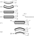
- FIG. 1 is a flowchart of a method for manufacturing an SOI wafer according to the present invention.
- an oxide film 2 'on the back surface is formed on the bond wafer 1 (FIG. 1A).
- a thermal oxide film is preferable.
- a thermal oxide film is formed on the entire surface of the bond wafer, and then the thermal oxide film on the bonding surface side of the bond wafer is removed.
- a method of producing a bond wafer having a thermal oxide film only on the back surface is preferable.
- a thermal oxide film having a substantially uniform thickness is formed on the entire surface of the bond wafer, and then a protective sheet such as a ring-shaped rubber (O-ring) or PVC is used. Then, with the oxide film on the back surface protected, the thermal oxide film on the bonding surface side is removed with an HF solution using a method of contacting the oxide film with an etchant or spin etching to leave only the oxide film on the back surface.
- a method can be mentioned.
- a silicon single crystal wafer as a semiconductor single crystal substrate used as a bond wafer. It can also be used.
- an oxide film 2 is further formed on the bond wafer 1 on which the oxide film 2 'on the back surface is formed (FIG. 1B).
- a thermal oxide film is preferable, and as a method for forming the oxide film, a method of thermally oxidizing the entire surface of the bond wafer on which the back oxide film is formed is preferable.
- a step of polishing the bonding surface side by CMP or the like may be added, and then the entire surface may be thermally oxidized (between (A) and (B) in FIG. 1). .
- a bond wafer having a thicker oxide film on the back surface than the oxide film on the bonded surface is manufactured by the method exemplified above. With such a bond wafer, even if a concave shape is formed in advance before being bonded to the base wafer or a later-described helium ion implantation layer is formed, it is possible to suppress more than necessary warpage.
- the thickness of the oxide film on the back surface is larger than the oxide film on the bonded surface.
- the specifications of the SOI wafer to be manufactured (diameter, base wafer thickness, BOX layer thickness, etc.) and the bond used Based on the wafer specifications (diameter, wafer thickness, etc.), the mismatch immediately after peeling is prevented (the size of the convex shape of the SOI wafer is equal to the size of the concave shape of the bond wafer after peeling). And can be set as appropriate by experiment or calculation.
- ions are implanted into the bonding surface side of the bond wafer 1 on which the oxide film 2 is formed to form an ion implantation layer (FIG. 1C).
- an ion-implanted layer include those formed by ion-implanting at least one gas ion of hydrogen and a rare gas, and in particular, a hydrogen ion-implanted layer formed by implanting hydrogen ions. Or a co-implanted layer formed by implanting both hydrogen ions and helium ions.
- the peeled bond wafer 101 ′ has a convex shape, A warp shape mismatch with the SOI wafer 120 occurred, and scratches and SOI film thickness abnormality occurred.
- the warp shape of the bond wafer can be set in advance before bonding by increasing the thickness of the oxide film on the back surface. The influence by can be suppressed to the minimum.
- the bonded wafer 1 is bonded to the surface of the base wafer 5 through the oxide film 2 at a room temperature of about 20 to 30 ° C., for example, to form a bonded wafer 10 (FIG. 1E). (F)).
- the bonding strength at room temperature can be improved by performing plasma treatment on the bonding surface of at least one of the bond wafer and the base wafer before bonding.
- the base wafer a silicon single crystal wafer, a silicon single crystal wafer having an insulating film formed on the surface, or the like can be used.
- An SOI wafer 20 having the following structure is formed (FIG. 1G).
- the peeled bond wafer 1 ′ is surely warped in a concave shape, and contact due to a mismatch in shape between the peeled bond wafer and the SOI wafer as in the prior art can be prevented.
- one of the features of the SOI wafer manufacturing method using the ion implantation separation method is that the bond wafer after separation can be reused. Therefore, also in the present invention, a wafer produced by regenerating the peeled bond wafer 1 'can be used. In this case, when the bond wafer after peeling is reprocessed, the bond wafer with the oxide film on the back surface is produced by regenerating without removing the oxide film on the back surface. A bond wafer in which the oxide film on the back surface is thicker than the oxide film on the mating surface can be manufactured.
- the removal of the oxide film remaining on the outer peripheral unbonded portion on the bonding surface side in the reclaim processing of the bonded wafer after peeling is achieved by directly polishing the bonding surface side.
- the protection of the back oxide film at the time of reprocessing the bonded wafer after peeling may be performed by blocking the etching solution or etching gas by O-ring as described above, or the bond after peeling the protective sheet such as PVC. It may be attached to the back surface of the wafer, or it may be prevented that the etching solution or etching gas flows around the back surface of the bond wafer due to centrifugal force or wind pressure generated by the rotation of the wafer.
- An HF solution is desirable as an etching solution for the oxide film. Etching may be performed with HF gas.
- the O-ring is preferably set to a few mm from the outer periphery so that warpage occurs in the bond wafer after etching. However, depending on the level of allowable warpage, the O-ring may be installed further inside.
- the oxide film of the bond wafer to be bonded to the base wafer is made thicker than the oxide film on the bonded surface, so that the shape of the bond wafer at the time of peeling is reliably deformed into a concave shape.
- contact between the bond wafer after peeling and the SOI wafer can be suppressed, and scratches and film thickness abnormalities of the SOI wafer can be suppressed.
- Example 1 A bond wafer made of a silicon single crystal wafer having a mirror polished surface of 300 mm in diameter is thermally oxidized to form a 150 nm thermal oxide film (initial oxide film) on the entire surface, and the oxide film on the back surface of the bond wafer is O-ringed. In a protected state, it is immersed in an aqueous HF solution to remove the oxide film on the bonding surface side, and after that, the surface is reprocessed by CMP processing, and then thermal oxidation is performed again to thermally bond 30 nm on the bonding surface side.
- Example 2 The bonded wafer (with a back oxide film of 155 nm) obtained in Example 1 was immersed in an HF aqueous solution in a state where the back oxide film (initial oxide film) was protected by O-ring, and the bonded surface side was bonded. After removing the oxide film, and then performing reprocessing by CMP processing, thermal oxidation is performed to form a 30 nm thermal oxide film (buried oxide film) on the bonding surface side, and hydrogen ion implantation is performed.
- the wafer was bonded to a base wafer made of a silicon single crystal wafer having a diameter of 300 mm, and peeled and heat treated in a horizontal heat treatment furnace to produce 10 SOI wafers.
- Example 3 A bond wafer made of a silicon single crystal wafer having a mirror polished surface of 300 mm in diameter is thermally oxidized to form a 150 nm thermal oxide film (initial oxide film) on the entire surface, and the oxide film on the back surface of the bond wafer is O-ringed. In a protected state, it is immersed in an aqueous HF solution to remove the oxide film on the bonding surface side, and after that, the surface is reprocessed by CMP processing, and then thermal oxidation is performed again to thermally bond 30 nm on the bonding surface side.
- a film (buried oxide film) and performing ion implantation (co-implantation) of hydrogen and helium
- it is bonded to a base wafer made of a silicon single crystal wafer having a diameter of 300 mm, and peeled off by a heat treatment in a horizontal heat treatment furnace.
- the implantation energies are 30 keV and 50 keV, respectively, so that helium ions are implanted deeper.
- thermo oxide film (embedded oxide film) is formed on the entire surface of a bond wafer made of a silicon single crystal wafer having a mirror polished surface of both sides with a diameter of 300 mm, and then hydrogen without performing HF treatment and re-forming the thermal oxide film. After performing the ion implantation, 10 SOI wafers were manufactured by bonding to a base wafer and peeling and heat treatment.
- thermo oxide film (embedded oxide film) is formed on the entire surface of a bond wafer made of a silicon single crystal wafer having a mirror polished surface of both sides with a diameter of 300 mm, and then hydrogen without performing HF treatment and re-forming the thermal oxide film.
- the wafer was bonded to a base wafer, peeled off by heat treatment, and 10 SOI wafers were produced.
- the implantation energies are 30 keV and 50 keV, respectively, so that helium ions are implanted deeper.
- Table 1 shows the manufacturing conditions of the SOI wafers of Examples 1 to 3 and Comparative Examples 1 and 2, the warped shapes of the bond wafer and the SOI wafer after peeling, the results of scratches and abnormal SOI film thickness.
- corrugation) of curvature shows the shape on the basis of a peeling surface.
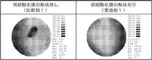
- Example 1 the warpage of the bond wafer and the SOI wafer after peeling was almost the same, and no scratch or SOI film thickness abnormality occurred (see FIG. 2).
- Comparative Example 1 the warpage of the SOI wafer was larger than the warpage of the bond wafer after peeling, and an SOI film thickness abnormality occurred (see FIG. 2).
- Comparative Example 2 the warp of the bonded wafer after peeling becomes large and convex with respect to the warp of the SOI wafer, and the SOI film thickness abnormality occurs. When the optical microscope is observed, scratches (scratches) are found in the thin film portion of the SOI layer. Observed (see FIG. 3).
- the SOI wafer manufacturing method of the present invention can suppress the SOI wafer scratch and SOI film thickness distribution abnormality caused by the contact between the bond wafer and the SOI wafer after peeling at the time of peeling. It was.
- this invention is not limited to the said embodiment.
- the above-described embodiment is an exemplification, and the present invention has any configuration that has substantially the same configuration as the technical idea described in the claims of the present invention and that exhibits the same effects. Are included in the technical scope.
Landscapes
- Element Separation (AREA)
- Chemical & Material Sciences (AREA)
- Chemical Kinetics & Catalysis (AREA)
- General Chemical & Material Sciences (AREA)
Abstract
Description
半導体単結晶基板からなるボンドウェーハに酸化膜を形成し、該酸化膜を通して水素および希ガスのうち少なくとも1種類のガスイオンをイオン注入して前記ボンドウェーハにイオン注入層を形成し、該ボンドウェーハのイオン注入した表面とベースウェーハ表面とを前記酸化膜を介して貼り合わせた後、前記イオン注入層で前記ボンドウェーハを剥離することによりSOIウェーハを作製するSOIウェーハの製造方法において、
前記ボンドウェーハに形成する酸化膜を、貼り合わせ面の酸化膜よりも背面の酸化膜を厚くすることを特徴とするSOIウェーハの製造方法を提供する。
半導体単結晶基板からなるボンドウェーハに酸化膜を形成し、該酸化膜を通して水素および希ガスのうち少なくとも1種類のガスイオンをイオン注入して前記ボンドウェーハにイオン注入層を形成し、該ボンドウェーハのイオン注入した表面とベースウェーハ表面とを前記酸化膜を介して貼り合わせた後、前記イオン注入層で前記ボンドウェーハを剥離することによりSOIウェーハを作製するSOIウェーハの製造方法において、
前記ボンドウェーハに形成する酸化膜を、貼り合わせ面の酸化膜よりも背面の酸化膜を厚くするSOIウェーハの製造方法である。
図1は、本発明のSOIウェーハの製造方法のフロー図である。
尚、ベースウェーハとしては、シリコン単結晶ウェーハ、又は、表面に絶縁膜を形成したシリコン単結晶ウェーハなどを用いることができる。
直径300mmの両面が鏡面研磨されたシリコン単結晶ウェーハからなるボンドウェーハに熱酸化を行って150nmの熱酸化膜(初期酸化膜)を全面に形成し、ボンドウェーハの背面の酸化膜をオーリングで保護した状態でHF水溶液に浸漬して貼り合わせ面側の酸化膜を除去し、その後、CMP加工により表面の再加工を行った後、再度、熱酸化を行い貼り合わせ面側に30nmの熱酸化膜(埋め込み酸化膜)を形成し、水素のイオン注入を行った後、直径300mmのシリコン単結晶ウェーハからなるベースウェーハと貼り合わせ、横型熱処理炉で剥離熱処理して剥離してSOIウェーハを10枚作製した。
実施例1で得られた剥離後のボンドウェーハ(背面の酸化膜155nm付き)を、背面の酸化膜(初期酸化膜)をオーリングで保護した状態でHF水溶液に浸漬して貼り合わせ面側の酸化膜を除去し、その後、CMP加工により再生加工を行った後、熱酸化を行い貼り合わせ面側に30nmの熱酸化膜(埋め込み酸化膜)を形成し、水素のイオン注入を行った後、直径300mmのシリコン単結晶ウェーハからなるベースウェーハと貼り合わせ、横型熱処理炉で剥離熱処理して剥離してSOIウェーハを10枚作製した。
直径300mmの両面が鏡面研磨されたシリコン単結晶ウェーハからなるボンドウェーハに熱酸化を行って150nmの熱酸化膜(初期酸化膜)を全面に形成し、ボンドウェーハの背面の酸化膜をオーリングで保護した状態でHF水溶液に浸漬して貼り合わせ面側の酸化膜を除去し、その後、CMP加工により表面の再加工を行った後、再度、熱酸化を行い貼り合わせ面側に30nmの熱酸化膜(埋め込み酸化膜)を形成し、水素及びヘリウムのイオン注入(共注入)を行った後、直径300mmのシリコン単結晶ウェーハからなるベースウェーハと貼り合わせ、横型熱処理炉で剥離熱処理して剥離してSOIウェーハを10枚作製した。
尚、水素及びヘリウムの共注入では、注入エネルギーがそれぞれ30keV、50keVであるため、ヘリウムイオンの方が深い位置に注入される。
直径300mmの両面が鏡面研磨されたシリコン単結晶ウェーハからなるボンドウェーハの全面に30nmの熱酸化膜(埋め込み酸化膜)を形成し、その後、HF処理及び再度の熱酸化膜形成を行わずに水素のイオン注入を行った後、ベースウェーハに貼り合わせ、剥離熱処理して剥離してSOIウェーハを10枚作製した。
直径300mmの両面が鏡面研磨されたシリコン単結晶ウェーハからなるボンドウェーハの全面に30nmの熱酸化膜(埋め込み酸化膜)を形成し、その後、HF処理及び再度の熱酸化膜形成を行わずに水素及びヘリウムのイオン注入(共注入)を行った後、ベースウェーハに貼り合わせ、剥離熱処理して剥離してSOIウェーハを10枚作製した。
尚、水素及びヘリウムの共注入では、注入エネルギーがそれぞれ30keV、50keVであるため、ヘリウムイオンの方が深い位置に注入される。
尚、反りの形状(凹凸)は、剥離面を基準とした形状のことを示す。

Claims (6)
- 半導体単結晶基板からなるボンドウェーハに酸化膜を形成し、該酸化膜を通して水素および希ガスのうち少なくとも1種類のガスイオンをイオン注入して前記ボンドウェーハにイオン注入層を形成し、該ボンドウェーハのイオン注入した表面とベースウェーハ表面とを前記酸化膜を介して貼り合わせた後、前記イオン注入層で前記ボンドウェーハを剥離することによりSOIウェーハを作製するSOIウェーハの製造方法において、
前記ボンドウェーハに形成する酸化膜を、貼り合わせ面の酸化膜よりも背面の酸化膜を厚くすることを特徴とするSOIウェーハの製造方法。 - 前記ボンドウェーハの酸化膜の形成は、ボンドウェーハの全面に熱酸化膜を形成した後、該ボンドウェーハの貼り合わせ面側の熱酸化膜を除去することによって背面のみに熱酸化膜を有するボンドウェーハを作製し、該背面のみに熱酸化膜を有するボンドウェーハの全面を熱酸化することによって行うことを特徴とする請求項1に記載のSOIウェーハの製造方法。
- 前記ボンドウェーハの貼り合わせ面側の熱酸化膜を除去した後に、該貼り合わせ面側を研磨する工程を含み、その後全面の熱酸化を行うことを特徴とする請求項2に記載のSOIウェーハの製造方法。
- 前記ボンドウェーハとして、イオン注入層で剥離後のボンドウェーハを再生加工して作製したウェーハを用いることを特徴とする請求項1乃至請求項3のいずれか一項に記載のSOIウェーハの製造方法。
- 前記再生加工において、前記剥離後のボンドウェーハの背面酸化膜を除去しないことを特徴とする請求項4に記載のSOIウェーハの製造方法。
- 前記イオン注入として、水素イオンとヘリウムイオンの共注入を行い、該共注入においてヘリウムイオンを水素イオンよりも深い位置に注入することを特徴とする請求項1乃至請求項5のいずれか一項に記載のSOIウェーハの製造方法。
Priority Applications (5)
| Application Number | Priority Date | Filing Date | Title |
|---|---|---|---|
| SG11201501873QA SG11201501873QA (en) | 2012-11-21 | 2013-10-11 | Method for manufacturing soi wafer |
| US14/427,151 US9378999B2 (en) | 2012-11-21 | 2013-10-11 | Method for manufacturing SOI wafer |
| KR1020157005866A KR101910100B1 (ko) | 2012-11-21 | 2013-10-11 | Soi 웨이퍼의 제조방법 |
| CN201380047666.6A CN104620384B (zh) | 2012-11-21 | 2013-10-11 | Soi晶圆的制造方法 |
| EP13856571.8A EP2924736B1 (en) | 2012-11-21 | 2013-10-11 | Method for manufacturing soi wafer |
Applications Claiming Priority (2)
| Application Number | Priority Date | Filing Date | Title |
|---|---|---|---|
| JP2012255719A JP5821828B2 (ja) | 2012-11-21 | 2012-11-21 | Soiウェーハの製造方法 |
| JP2012-255719 | 2012-11-21 |
Publications (1)
| Publication Number | Publication Date |
|---|---|
| WO2014080563A1 true WO2014080563A1 (ja) | 2014-05-30 |
Family
ID=50775761
Family Applications (1)
| Application Number | Title | Priority Date | Filing Date |
|---|---|---|---|
| PCT/JP2013/006072 Ceased WO2014080563A1 (ja) | 2012-11-21 | 2013-10-11 | Soiウェーハの製造方法 |
Country Status (7)
| Country | Link |
|---|---|
| US (1) | US9378999B2 (ja) |
| EP (1) | EP2924736B1 (ja) |
| JP (1) | JP5821828B2 (ja) |
| KR (1) | KR101910100B1 (ja) |
| CN (1) | CN104620384B (ja) |
| SG (1) | SG11201501873QA (ja) |
| WO (1) | WO2014080563A1 (ja) |
Families Citing this family (7)
| Publication number | Priority date | Publication date | Assignee | Title |
|---|---|---|---|---|
| JP6353814B2 (ja) * | 2015-06-09 | 2018-07-04 | 信越半導体株式会社 | 貼り合わせsoiウェーハの製造方法 |
| JP6556511B2 (ja) * | 2015-06-17 | 2019-08-07 | ルネサスエレクトロニクス株式会社 | 半導体装置の製造方法 |
| CN110085549B (zh) * | 2018-01-26 | 2021-06-04 | 沈阳硅基科技有限公司 | 一种双面注入得到soi的方法 |
| CN110544668B (zh) * | 2018-05-28 | 2022-03-25 | 沈阳硅基科技有限公司 | 一种通过贴膜改变soi边缘stir的方法 |
| CN109360805A (zh) * | 2018-09-28 | 2019-02-19 | 沈阳硅基科技有限公司 | 一种图形soi硅片的制备方法 |
| CN115188703B (zh) * | 2022-05-16 | 2025-09-19 | 绍兴中芯集成电路制造股份有限公司 | 一种soi晶圆及制造方法 |
| FR3146019A1 (fr) * | 2023-02-16 | 2024-08-23 | Soitec | Procédé de formation d’une zone de fragisilation dans un substrat semi-conducteur |
Citations (8)
| Publication number | Priority date | Publication date | Assignee | Title |
|---|---|---|---|---|
| JPH0355822A (ja) | 1989-07-25 | 1991-03-11 | Shin Etsu Handotai Co Ltd | 半導体素子形成用基板の製造方法 |
| JPH03250615A (ja) * | 1990-02-28 | 1991-11-08 | Shin Etsu Handotai Co Ltd | 接合ウエーハの製造方法 |
| JPH1126336A (ja) * | 1997-07-08 | 1999-01-29 | Sumitomo Metal Ind Ltd | 貼り合わせ半導体基板及びその製造方法 |
| JP2004503111A (ja) * | 2000-07-12 | 2004-01-29 | コミツサリア タ レネルジー アトミーク | 材料ブロックを切り取るための方法ならびに薄膜の形成方法 |
| JP2006270039A (ja) * | 2005-02-28 | 2006-10-05 | Shin Etsu Handotai Co Ltd | 貼り合わせウエーハの製造方法及び貼り合わせウエーハ |
| JP2008140878A (ja) | 2006-11-30 | 2008-06-19 | Sumco Corp | シリコンウェーハ及びその製造方法並びに貼り合わせsoiウェーハ及びその製造方法。 |
| JP2011187502A (ja) * | 2010-03-04 | 2011-09-22 | Seiko Epson Corp | 半導体装置の製造方法 |
| WO2012012138A2 (en) * | 2010-06-30 | 2012-01-26 | Corning Incorporated | Method for finishing silicon on insulator substrates |
Family Cites Families (4)
| Publication number | Priority date | Publication date | Assignee | Title |
|---|---|---|---|---|
| JP3500063B2 (ja) * | 1998-04-23 | 2004-02-23 | 信越半導体株式会社 | 剥離ウエーハを再利用する方法および再利用に供されるシリコンウエーハ |
| US20070069335A1 (en) * | 2003-09-08 | 2007-03-29 | Akihiko Endo | Bonded wafer and its manufacturing method |
| CN101124657B (zh) * | 2005-02-28 | 2010-04-14 | 信越半导体股份有限公司 | 贴合晶圆的制造方法及贴合晶圆 |
| US7902039B2 (en) | 2006-11-30 | 2011-03-08 | Sumco Corporation | Method for manufacturing silicon wafer |
-
2012
- 2012-11-21 JP JP2012255719A patent/JP5821828B2/ja active Active
-
2013
- 2013-10-11 CN CN201380047666.6A patent/CN104620384B/zh active Active
- 2013-10-11 KR KR1020157005866A patent/KR101910100B1/ko active Active
- 2013-10-11 US US14/427,151 patent/US9378999B2/en active Active
- 2013-10-11 EP EP13856571.8A patent/EP2924736B1/en active Active
- 2013-10-11 SG SG11201501873QA patent/SG11201501873QA/en unknown
- 2013-10-11 WO PCT/JP2013/006072 patent/WO2014080563A1/ja not_active Ceased
Patent Citations (8)
| Publication number | Priority date | Publication date | Assignee | Title |
|---|---|---|---|---|
| JPH0355822A (ja) | 1989-07-25 | 1991-03-11 | Shin Etsu Handotai Co Ltd | 半導体素子形成用基板の製造方法 |
| JPH03250615A (ja) * | 1990-02-28 | 1991-11-08 | Shin Etsu Handotai Co Ltd | 接合ウエーハの製造方法 |
| JPH1126336A (ja) * | 1997-07-08 | 1999-01-29 | Sumitomo Metal Ind Ltd | 貼り合わせ半導体基板及びその製造方法 |
| JP2004503111A (ja) * | 2000-07-12 | 2004-01-29 | コミツサリア タ レネルジー アトミーク | 材料ブロックを切り取るための方法ならびに薄膜の形成方法 |
| JP2006270039A (ja) * | 2005-02-28 | 2006-10-05 | Shin Etsu Handotai Co Ltd | 貼り合わせウエーハの製造方法及び貼り合わせウエーハ |
| JP2008140878A (ja) | 2006-11-30 | 2008-06-19 | Sumco Corp | シリコンウェーハ及びその製造方法並びに貼り合わせsoiウェーハ及びその製造方法。 |
| JP2011187502A (ja) * | 2010-03-04 | 2011-09-22 | Seiko Epson Corp | 半導体装置の製造方法 |
| WO2012012138A2 (en) * | 2010-06-30 | 2012-01-26 | Corning Incorporated | Method for finishing silicon on insulator substrates |
Non-Patent Citations (1)
| Title |
|---|
| See also references of EP2924736A4 |
Also Published As
| Publication number | Publication date |
|---|---|
| JP2014103329A (ja) | 2014-06-05 |
| JP5821828B2 (ja) | 2015-11-24 |
| EP2924736A1 (en) | 2015-09-30 |
| EP2924736B1 (en) | 2017-08-30 |
| US20150243550A1 (en) | 2015-08-27 |
| SG11201501873QA (en) | 2015-05-28 |
| EP2924736A4 (en) | 2016-06-29 |
| KR20150087181A (ko) | 2015-07-29 |
| KR101910100B1 (ko) | 2018-10-19 |
| CN104620384B (zh) | 2017-06-06 |
| US9378999B2 (en) | 2016-06-28 |
| CN104620384A (zh) | 2015-05-13 |
Similar Documents
| Publication | Publication Date | Title |
|---|---|---|
| JP5780234B2 (ja) | Soiウェーハの製造方法 | |
| JP5821828B2 (ja) | Soiウェーハの製造方法 | |
| WO2013102968A1 (ja) | 貼り合わせsoiウェーハの製造方法 | |
| CN101124657B (zh) | 贴合晶圆的制造方法及贴合晶圆 | |
| JP6380245B2 (ja) | Soiウェーハの製造方法 | |
| JP6056516B2 (ja) | Soiウェーハの製造方法及びsoiウェーハ | |
| WO2015136834A1 (ja) | 貼り合わせsoiウェーハの製造方法 | |
| JP5862521B2 (ja) | Soiウェーハの製造方法 | |
| KR102095383B1 (ko) | 접합 웨이퍼의 제조방법 | |
| CN104364880B (zh) | Soi晶片的制造方法 | |
| JP2005079389A (ja) | 貼り合わせウェーハの分離方法及びその分離用ボート | |
| JP5564785B2 (ja) | 貼り合わせ基板の製造方法 | |
| JP6607207B2 (ja) | 貼り合わせsoiウェーハの製造方法 | |
| JP6136786B2 (ja) | 貼り合わせウェーハの製造方法 | |
| JP2009252948A (ja) | 貼り合わせウェーハの製造方法 |
Legal Events
| Date | Code | Title | Description |
|---|---|---|---|
| 121 | Ep: the epo has been informed by wipo that ep was designated in this application |
Ref document number: 13856571 Country of ref document: EP Kind code of ref document: A1 |
|
| ENP | Entry into the national phase |
Ref document number: 20157005866 Country of ref document: KR Kind code of ref document: A |
|
| REEP | Request for entry into the european phase |
Ref document number: 2013856571 Country of ref document: EP |
|
| WWE | Wipo information: entry into national phase |
Ref document number: 2013856571 Country of ref document: EP |
|
| WWE | Wipo information: entry into national phase |
Ref document number: 14427151 Country of ref document: US |
|
| NENP | Non-entry into the national phase |
Ref country code: DE |