WO2014080754A1 - 電磁波吸収フィルム及びその製造方法 - Google Patents
電磁波吸収フィルム及びその製造方法 Download PDFInfo
- Publication number
- WO2014080754A1 WO2014080754A1 PCT/JP2013/079863 JP2013079863W WO2014080754A1 WO 2014080754 A1 WO2014080754 A1 WO 2014080754A1 JP 2013079863 W JP2013079863 W JP 2013079863W WO 2014080754 A1 WO2014080754 A1 WO 2014080754A1
- Authority
- WO
- WIPO (PCT)
- Prior art keywords
- electromagnetic wave
- wave absorbing
- fine particles
- graphene fine
- graphene
- Prior art date
- Legal status (The legal status is an assumption and is not a legal conclusion. Google has not performed a legal analysis and makes no representation as to the accuracy of the status listed.)
- Ceased
Links
Images


Classifications
-
- C—CHEMISTRY; METALLURGY
- C09—DYES; PAINTS; POLISHES; NATURAL RESINS; ADHESIVES; COMPOSITIONS NOT OTHERWISE PROVIDED FOR; APPLICATIONS OF MATERIALS NOT OTHERWISE PROVIDED FOR
- C09D—COATING COMPOSITIONS, e.g. PAINTS, VARNISHES OR LACQUERS; FILLING PASTES; CHEMICAL PAINT OR INK REMOVERS; INKS; CORRECTING FLUIDS; WOODSTAINS; PASTES OR SOLIDS FOR COLOURING OR PRINTING; USE OF MATERIALS THEREFOR
- C09D7/00—Features of coating compositions, not provided for in group C09D5/00; Processes for incorporating ingredients in coating compositions
- C09D7/40—Additives
- C09D7/60—Additives non-macromolecular
- C09D7/61—Additives non-macromolecular inorganic
-
- B—PERFORMING OPERATIONS; TRANSPORTING
- B05—SPRAYING OR ATOMISING IN GENERAL; APPLYING FLUENT MATERIALS TO SURFACES, IN GENERAL
- B05D—PROCESSES FOR APPLYING FLUENT MATERIALS TO SURFACES, IN GENERAL
- B05D3/00—Pretreatment of surfaces to which liquids or other fluent materials are to be applied; After-treatment of applied coatings, e.g. intermediate treating of an applied coating preparatory to subsequent applications of liquids or other fluent materials
- B05D3/007—After-treatment
-
- C—CHEMISTRY; METALLURGY
- C09—DYES; PAINTS; POLISHES; NATURAL RESINS; ADHESIVES; COMPOSITIONS NOT OTHERWISE PROVIDED FOR; APPLICATIONS OF MATERIALS NOT OTHERWISE PROVIDED FOR
- C09D—COATING COMPOSITIONS, e.g. PAINTS, VARNISHES OR LACQUERS; FILLING PASTES; CHEMICAL PAINT OR INK REMOVERS; INKS; CORRECTING FLUIDS; WOODSTAINS; PASTES OR SOLIDS FOR COLOURING OR PRINTING; USE OF MATERIALS THEREFOR
- C09D133/00—Coating compositions based on homopolymers or copolymers of compounds having one or more unsaturated aliphatic radicals, each having only one carbon-to-carbon double bond, and at least one being terminated by only one carboxyl radical, or of salts, anhydrides, esters, amides, imides, or nitriles thereof; Coating compositions based on derivatives of such polymers
- C09D133/04—Homopolymers or copolymers of esters
- C09D133/06—Homopolymers or copolymers of esters of esters containing only carbon, hydrogen and oxygen, the oxygen atom being present only as part of the carboxyl radical
- C09D133/10—Homopolymers or copolymers of methacrylic acid esters
- C09D133/12—Homopolymers or copolymers of methyl methacrylate
-
- C—CHEMISTRY; METALLURGY
- C09—DYES; PAINTS; POLISHES; NATURAL RESINS; ADHESIVES; COMPOSITIONS NOT OTHERWISE PROVIDED FOR; APPLICATIONS OF MATERIALS NOT OTHERWISE PROVIDED FOR
- C09D—COATING COMPOSITIONS, e.g. PAINTS, VARNISHES OR LACQUERS; FILLING PASTES; CHEMICAL PAINT OR INK REMOVERS; INKS; CORRECTING FLUIDS; WOODSTAINS; PASTES OR SOLIDS FOR COLOURING OR PRINTING; USE OF MATERIALS THEREFOR
- C09D5/00—Coating compositions, e.g. paints, varnishes or lacquers, characterised by their physical nature or the effects produced; Filling pastes
- C09D5/32—Radiation-absorbing paints
-
- C—CHEMISTRY; METALLURGY
- C09—DYES; PAINTS; POLISHES; NATURAL RESINS; ADHESIVES; COMPOSITIONS NOT OTHERWISE PROVIDED FOR; APPLICATIONS OF MATERIALS NOT OTHERWISE PROVIDED FOR
- C09D—COATING COMPOSITIONS, e.g. PAINTS, VARNISHES OR LACQUERS; FILLING PASTES; CHEMICAL PAINT OR INK REMOVERS; INKS; CORRECTING FLUIDS; WOODSTAINS; PASTES OR SOLIDS FOR COLOURING OR PRINTING; USE OF MATERIALS THEREFOR
- C09D7/00—Features of coating compositions, not provided for in group C09D5/00; Processes for incorporating ingredients in coating compositions
- C09D7/20—Diluents or solvents
-
- C—CHEMISTRY; METALLURGY
- C09—DYES; PAINTS; POLISHES; NATURAL RESINS; ADHESIVES; COMPOSITIONS NOT OTHERWISE PROVIDED FOR; APPLICATIONS OF MATERIALS NOT OTHERWISE PROVIDED FOR
- C09D—COATING COMPOSITIONS, e.g. PAINTS, VARNISHES OR LACQUERS; FILLING PASTES; CHEMICAL PAINT OR INK REMOVERS; INKS; CORRECTING FLUIDS; WOODSTAINS; PASTES OR SOLIDS FOR COLOURING OR PRINTING; USE OF MATERIALS THEREFOR
- C09D7/00—Features of coating compositions, not provided for in group C09D5/00; Processes for incorporating ingredients in coating compositions
- C09D7/40—Additives
- C09D7/66—Additives characterised by particle size
- C09D7/69—Particle size larger than 1000 nm
-
- H—ELECTRICITY
- H04—ELECTRIC COMMUNICATION TECHNIQUE
- H04B—TRANSMISSION
- H04B1/00—Details of transmission systems, not covered by a single one of groups H04B3/00 - H04B13/00; Details of transmission systems not characterised by the medium used for transmission
- H04B1/38—Transceivers, i.e. devices in which transmitter and receiver form a structural unit and in which at least one part is used for functions of transmitting and receiving
- H04B1/3827—Portable transceivers
- H04B1/3833—Hand-held transceivers
- H04B1/3838—Arrangements for reducing RF exposure to the user, e.g. by changing the shape of the transceiver while in use
-
- H—ELECTRICITY
- H04—ELECTRIC COMMUNICATION TECHNIQUE
- H04B—TRANSMISSION
- H04B1/00—Details of transmission systems, not covered by a single one of groups H04B3/00 - H04B13/00; Details of transmission systems not characterised by the medium used for transmission
- H04B1/38—Transceivers, i.e. devices in which transmitter and receiver form a structural unit and in which at least one part is used for functions of transmitting and receiving
- H04B1/40—Circuits
- H04B1/50—Circuits using different frequencies for the two directions of communication
- H04B1/52—Hybrid arrangements, i.e. arrangements for transition from single-path two-direction transmission to single-direction transmission on each of two paths or vice versa
- H04B1/525—Hybrid arrangements, i.e. arrangements for transition from single-path two-direction transmission to single-direction transmission on each of two paths or vice versa with means for reducing leakage of transmitter signal into the receiver
-
- H—ELECTRICITY
- H05—ELECTRIC TECHNIQUES NOT OTHERWISE PROVIDED FOR
- H05K—PRINTED CIRCUITS; CASINGS OR CONSTRUCTIONAL DETAILS OF ELECTRIC APPARATUS; MANUFACTURE OF ASSEMBLAGES OF ELECTRICAL COMPONENTS
- H05K9/00—Screening of apparatus or components against electric or magnetic fields
- H05K9/0073—Shielding materials
- H05K9/0081—Electromagnetic shielding materials, e.g. EMI, RFI shielding
- H05K9/009—Electromagnetic shielding materials, e.g. EMI, RFI shielding comprising electro-conductive fibres, e.g. metal fibres, carbon fibres, metallised textile fibres, electro-conductive mesh, woven, non-woven mat, fleece, cross-linked
-
- C—CHEMISTRY; METALLURGY
- C01—INORGANIC CHEMISTRY
- C01B—NON-METALLIC ELEMENTS; COMPOUNDS THEREOF; METALLOIDS OR COMPOUNDS THEREOF NOT COVERED BY SUBCLASS C01C
- C01B2204/00—Structure or properties of graphene
- C01B2204/04—Specific amount of layers or specific thickness
-
- C—CHEMISTRY; METALLURGY
- C01—INORGANIC CHEMISTRY
- C01B—NON-METALLIC ELEMENTS; COMPOUNDS THEREOF; METALLOIDS OR COMPOUNDS THEREOF NOT COVERED BY SUBCLASS C01C
- C01B2204/00—Structure or properties of graphene
- C01B2204/20—Graphene characterized by its properties
- C01B2204/32—Size or surface area
-
- C—CHEMISTRY; METALLURGY
- C08—ORGANIC MACROMOLECULAR COMPOUNDS; THEIR PREPARATION OR CHEMICAL WORKING-UP; COMPOSITIONS BASED THEREON
- C08K—Use of inorganic or non-macromolecular organic substances as compounding ingredients
- C08K3/00—Use of inorganic substances as compounding ingredients
- C08K3/02—Elements
- C08K3/04—Carbon
- C08K3/042—Graphene or derivatives, e.g. graphene oxides
Definitions
- the present invention relates to an electromagnetic wave absorbing film that can efficiently absorb electromagnetic waves of several hundred MHz to several GHz in the near field in portable information terminals such as mobile phones and smartphones, electronic devices such as personal computers, and the like, and a manufacturing method thereof.
- Japanese Patent Application Laid-Open No. 2010-153542 discloses a base material, a conductive layer made of a conductive coating material containing metal or carbon particles such as Cu, scales, or fine wires, and a soft magnetic material such as ferrite, sendust, and permalloy.
- the electromagnetic wave electromagnetic wave absorption film which has a magnetic layer which consists of a magnetic coating material containing is disclosed.
- the electromagnetic wave absorbing film disclosed in Japanese Patent Application Laid-Open No. 2010-153542 is expensive because it has a conductive layer and a magnetic layer, and has sufficient absorbing ability for electromagnetic noise of several hundred MHz to several GHz. Absent.
- JP-A-2006-114877 states that (a) ⁇ ⁇ ⁇ carbon nanotubes, carbon nanohorns, graphite nanos on (b) carbon nanotubes, carbon nanohorns, graphite nano 100 parts by weight of carbon nanomaterials such as fiber and carbon nanofiber, (c) heat of thermoplastic resin such as ABS resin, polyvinylidene fluoride, polyamide, polyimide, polyethylene terephthalate, polycarbonate, polyvinyl chloride, epoxy resin, phenol resin, etc.
- thermoplastic resin such as ABS resin, polyvinylidene fluoride, polyamide, polyimide, polyethylene terephthalate, polycarbonate, polyvinyl chloride, epoxy resin, phenol resin, etc.
- a curable resin or a resin component made of a UV curable resin such as polyester, polyvinyl butyral, acrylic, phenol, polyurethane, and (d) a ketone, saturated hydrocarbon, aromatic hydrocarbon, glycol Ethers, glycol ether esthetics S
- the electromagnetic wave absorbing sheet disclosed in Japanese Patent Application Laid-Open No. 2006-114877 does not have sufficient absorbing ability for electromagnetic noise of several hundred MHz to several GHz.
- an object of the present invention is to provide an electromagnetic wave absorbing film having a high absorption ability for electromagnetic noise of several hundred MHz to several GHz and suitable for a portable information terminal, an electronic device, and the like, and a method for manufacturing the same. .
- flaky graphene fine particles have an electromagnetic wave absorption ability superior to that of carbon black and carbon nanotubes, but are likely to aggregate. Therefore, when a dilute solution in which flaky graphene fine particles are uniformly dispersed is applied to a plastic film in small portions in several batches, and drying is performed for each application process, aggregation of the flaky graphene fine particles is prevented.
- the inventors have found that an electromagnetic wave absorbing layer having a necessary thickness can be formed, and have arrived at the present invention.
- the electromagnetic wave absorbing film of the present invention comprises an electromagnetic wave absorbing layer containing flaky graphene fine particles and a binder resin on one surface of a plastic film, and the thickness of the electromagnetic wave absorbing layer is 2 to 15 g / m. 2 (represented by the weight of graphene fine particles per 1 m 2 ), the mass ratio of the binder resin to the graphene fine particles in the electromagnetic wave absorbing layer is 0.05 to 1, and the graphene fine particles are not present in the electromagnetic wave absorbing layer The total area ratio of the regions is 5% or less.
- the graphene fine particles preferably have an average diameter of 5 to 100 ⁇ m and an average thickness of 5 to 50 nm.
- the binder resin is preferably acrylic resin, polystyrene resin or polyvinyl alcohol.
- the method of the present invention for producing the electromagnetic wave absorbing film includes a step of applying an organic solvent dispersion containing 1 to 10% by mass of graphene fine particles and 0.05 to 5% by mass of a binder resin to one surface of a plastic film and then drying. Repeated multiple times.
- the mass ratio of the binder resin to the graphene fine particles is preferably 0.05 to 1.
- the coating amount of the dispersion once is preferably 1 to 3.5 g / m 2 (expressed by the weight of graphene fine particles per 1 m 2 ).
- the organic solvent is preferably at least one selected from the group consisting of ketones, aromatic hydrocarbons and alcohols.
- the drying step is preferably performed by heating to 30 to 100 ° C.
- the electromagnetic wave absorbing film of the present invention has an electromagnetic wave absorbing layer containing flaky graphene fine particles that are uniformly dispersed. Therefore, the electromagnetic wave absorbing film has high absorption capability for electromagnetic noise of several hundred MHz to several GHz, and uneven absorption capability. There is no. Therefore, even if it cuts and uses to a desired size, there is no variation and it can exhibit the outstanding electromagnetic wave absorption ability.
- the electromagnetic wave absorbing film of the present invention having such characteristics is effective in absorbing electromagnetic noise of several hundred MHz to several GHz in the near field in various portable information terminals such as mobile phones and smartphones and electronic devices such as personal computers. It is.
- FIG. 13 (a) is a partial cross-sectional front view showing the electromagnetic wave absorbing ability evaluation system shown in FIG.
- Example 2 About the electromagnetic wave absorption film of Example 1 and Example 2, the relationship between the thickness of the electromagnetic wave absorption layer (expressed by the weight of graphene fine particles per 1 m 2 ) and the average S 11 in the range of 1 to 6 GHz is shown. It is a graph. 3 is a graph showing P loss / P in at 0.1 to 6 GHz of the electromagnetic wave absorbing film laminate of Example 1 (the thickness of the electromagnetic wave absorbing layer: 6.0 g / m 2 , Sample 12). 4 is a scanning electron micrograph of the electromagnetic wave absorbing layer of Sample 35 in Example 3. 6 is a graph showing the surface roughness of the electromagnetic wave absorption layer of Sample 35 of Example 3 measured by a scanning electron microscope.
- Example 3 Regarding the electromagnetic wave absorbing films of Example 3 and Example 4, the relationship between the thickness of the electromagnetic wave absorbing layer (expressed by the weight of graphene fine particles per m 2 ) and the average S 11 in the range of 1 to 6 GHz is shown. It is a graph. 6 is a graph showing P loss / P in at 0.1 to 6 GHz of the electromagnetic wave absorption film laminate of Example 3 (electromagnetic wave absorption layer thickness: 6.0 g / m 2 , sample 32).
- FIG. 5 is a graph showing the relationship between the thickness of the electromagnetic wave absorbing layer (expressed by the weight of graphene fine particles per 1 m 2 ) and the average S 11 in the range of 1 to 6 GHz for the electromagnetic wave absorbing films of Examples 5 to 9. is there.
- Example 11 and Example 12 Regarding the electromagnetic wave absorbing films of Example 11 and Example 12, the relationship between the thickness of the electromagnetic wave absorbing layer (expressed by the weight of graphene fine particles per m 2 ) and the average S 11 in the range of 1 to 6 GHz is shown. It is a graph. 14 is a graph showing the surface roughness of the electromagnetic wave absorption layer of Sample 134 of Example 13 measured by a scanning electron microscope. About the electromagnetic wave absorption film of Example 13 and Example 14, the relationship between the thickness of the electromagnetic wave absorption layer (expressed by the weight of graphene fine particles per 1 m 2 ) and the average S 11 in the range of 1 to 6 GHz is shown. It is a graph. 2 is a scanning electron micrograph of an electromagnetic wave absorbing layer of Comparative Example 1. 3 is a graph showing the surface roughness of the electromagnetic wave absorption layer of Comparative Example 1 measured by a scanning electron microscope.
- Electromagnetic wave absorbing film As shown in FIG. 1, the electromagnetic wave absorbing film 1 of the present invention comprises a plastic film 11 and an electromagnetic wave absorbing layer 12 formed on one surface thereof.
- the resin forming the plastic film 11 is not particularly limited as long as it has insulation, sufficient strength, flexibility, and processability.
- polyester polyethylene terephthalate, etc.
- polyarylene sulfide polyphenylene sulfide, etc.
- Polyether sulfone polyether ether ketone
- polycarbonate acrylic resin
- acrylic resin polyamide, polyimide, polystyrene, polyolefin (polyethylene, polypropylene, etc.) and the like.
- the thickness of the plastic film 10 may be about 10 to 50 ⁇ m.
- the electromagnetic wave absorbing layer 12 is composed of graphene fine particles bonded by a binder resin.
- the flaky graphene fine particles 31 have a plate-like structure in which benzene rings are two-dimensionally connected, and may be either a single layer or a multi-layer. Multilayer is preferable. Since the graphene fine particles 31 have a hexagonal lattice structure, each carbon atom is bonded to three carbon atoms, and one of the four outer electrons used for the chemical bond is in a free state (free electrons and Become). Since free electrons can move along the crystal lattice, the graphene fine particles 31 have high conductivity.
- the diameter is the diameter of the plate surface portion.
- the diameter of the graphene fine particles 31 is defined as the diameter d of a circle having the same area S. Since the size of each graphene fine particle is represented by the diameter d and the thickness t, the average diameter of the used graphene fine particles is represented by ( ⁇ d) / n (where n is the number of measured graphene fine particles), and the average thickness Is represented by ( ⁇ t) / n.
- the diameter d and thickness t of the graphene fine particles can be obtained by image processing of a micrograph of the graphene fine particles.
- the average diameter of the graphene fine particles used in the present invention may be in the range of 5 to 100 ⁇ m.
- the preferred average diameter of the graphene fine particles is 5 to 50 ⁇ m, more preferably 10 to 30 ⁇ m.
- the average thickness of the graphene fine particles may be in the range of 5 to 50 nm.
- the average thickness of the graphene fine particles is less than 5 mm, the surface resistance of the electromagnetic wave absorption layer is increased by the binder resin interposed between the graphene fine particles, and a large amount of graphene fine particles must be used to reduce the surface resistance. It is not economical.
- the average thickness of the graphene fine particles is more than 50 nm, the graphene fine particles are easily destroyed when the graphene fine particles are uniformly dispersed in the solvent.
- a preferable average thickness of the graphene fine particles is 5 to 30 nm, and a more preferable average thickness is 10 to 25 nm.
- thermoplastic resin is a thermosetting resin (photo-curable resin). But it ’s okay.
- thermoplastic resin include acrylic resins such as polymethyl acrylate and polymethyl methacrylate, polystyrene, polycarbonate, polyvinyl chloride, and ABS resin, among which polymethyl methacrylate and polystyrene are preferable.
- thermosetting resins include epoxy resins, phenol resins, unsaturated polyester resins, alkyd resins, and polyurethanes.
- photocurable resin that can be used in the present invention include diacrylates and triacrylates. In the case of a thermosetting resin and a photocurable resin, it is preferably dissolved in an organic solvent in an oligomer state.
- the binder resin / graphene fine particle mass ratio is preferably 1 or less, and more preferably 0.5 or less.
- the lower limit of the mass ratio of the binder resin / graphene fine particles is preferably 0.05, more preferably 0.1, and most preferably 0.3.
- the distribution of the graphene fine particles in the electromagnetic wave absorbing layer is as follows: (1) the area ratio of the area where the graphene fine particles do not exist, determined from the micrograph of the electromagnetic wave absorbing layer, (2) the surface roughness of the electromagnetic wave absorbing layer, and (3) the electromagnetic wave absorbing layer The light transmittance can be evaluated.
- the electromagnetic wave absorbing layer 12 in which the graphene fine particles are aggregated has a graphene fine particle aggregation region 33 and a region 34 where no graphene fine particles are present. This can be easily confirmed by an electron micrograph.
- the area of the agglomeration zone 33 of graphene particles and S 1 when the area of a region having no graphene particles and S 2, the area ratio Rs of a region having no graphene particles S 2 / (S 1 + S 2) ⁇ 100 ( %).
- the area ratio of the region where the graphene fine particles are not present is obtained. If this area ratio is within 5%, it can be said that the dispersion of the graphene fine particles is good.
- the area ratio of the region where the graphene fine particles are not present is preferably within 2%, more preferably 0%.
- FIG. 5 shows a method for measuring the thickness distribution of the electromagnetic wave absorbing layer 12.
- a test piece of the electromagnetic wave absorbing film 1 having a predetermined size is placed on a flat base, and the surface roughness is measured along arbitrary straight lines L 1 , L 2 .
- FIG. 6 (a) shows the surface roughness Ra of the electromagnetic wave absorbing layer in which the graphene fine particles are not aggregated
- FIG. 6 (b) shows the surface roughness Ra of the electromagnetic wave absorbing layer in which the graphene fine particles are aggregated. Any surface roughness Ra is smoothed.
- the average thickness unevenness is within 20 ⁇ m, it can be said that the distribution of graphene fine particles is sufficiently uniform.
- the number n of straight lines to be measured is 3 or more, preferably 5 or more.
- the average thickness unevenness is preferably within 15 ⁇ m, more preferably within 10 ⁇ m, and most preferably within 5 ⁇ m.
- the surface roughness Ra of the electromagnetic wave absorbing layer 12 can be measured using a stylus type surface roughness measuring instrument or a scanning electron microscope (SEM).
- the uniformity of the distribution of the graphene fine particles can also be obtained from the light transmittance of the electromagnetic wave absorbing film 1.
- the total light transmittance is 0%.
- the degree of aggregation of the graphene fine particles can be evaluated by comparing the light transmittance. The light transmittance is measured on a plurality of test pieces arbitrarily cut from the electromagnetic wave absorbing film 1, and the measured values are averaged.
- the surface resistance of the electromagnetic wave absorbing layer 12 is preferably 50 to 250 ⁇ / ⁇ , more preferably 100 to 200 ⁇ / ⁇ , in order to exhibit sufficient electromagnetic wave absorbing ability.
- the surface resistance is measured by a DC two-terminal method on a square test piece of the electromagnetic wave absorption film 1 of 10 cm ⁇ 10 cm.
- the surface resistance of the electromagnetic wave absorbing layer 12 is reduced when the distribution of the graphene fine particles is uniform.
- the surface resistance of the electromagnetic wave absorbing layer 12 depends on the amount of graphene fine particles per unit area, and the thickness of the electromagnetic wave absorbing layer 12 is determined by the amount of graphene fine particles. Therefore, the thickness of the electromagnetic wave absorption layer 12 having the desired surface resistance is represented by the amount per unit area of the graphene fine particles.
- the thickness of the electromagnetic wave absorbing layer 12 expressed by the amount of graphene fine particles per unit area is preferably 2 to 15 g / m 2 , more preferably 3 to 12 g / m 2 , and most preferably 4 to 8 g. a / m 2.
- Protective film A protective film is preferably formed on the electromagnetic wave absorbing layer 12 in order to prevent the graphene fine particles from falling off.
- the protective film itself may be made of the same polymer as the plastic film constituting the electromagnetic wave absorbing film 1.
- the protective film can be bonded with an adhesive, but heat fusion is preferable for the purpose of simplifying the bonding.
- the protective film 1 ′ is formed by forming a heat-sealing layer 13 ′ on a plastic film 11 ′. In order to improve the adhesion to the protective film 1 ′, it is preferable to provide the heat fusion layer 13 also on the plastic film 11 of the electromagnetic wave absorbing film 1.
- Each of the heat-sealing layers 13 and 13 ′ can be formed of polyethylene having a low melting point such as an ethylene / ⁇ -olefin copolymer.
- a dispersion containing graphene fine particles, a binder resin and an organic solvent is preferably prepared by mixing an organic solvent solution of a binder resin with an organic solvent dispersion of graphene fine particles. This is because the graphene fine particles are likely to aggregate, and if the graphene fine particles and the binder resin are simultaneously mixed in an organic solvent, the graphene fine particles may be aggregated.
- the concentration of the graphene fine particles is preferably 1 to 10% by mass, more preferably 1 to 8% by mass, most preferably 2 to 8% by mass, particularly 2 to 7% by mass is preferred.
- the mass ratio of the binder resin / graphene fine particles is preferably 0.05 to 1, more preferably 0.05 to 0.5, and most preferably 0.1 to 0.5.
- the organic solvent used in the dispersion is preferably an organic solvent that easily disperses graphene fine particles, dissolves the binder resin, and easily evaporates in order to shorten the drying time.
- organic solvents include ketones such as methyl ethyl ketone, aliphatic hydrocarbons such as hexane, aromatic hydrocarbons such as xylene, and alcohols such as isopropyl alcohol. Of these, methyl ethyl ketone, xylene and the like are preferable. These may be used alone or in combination.
- the graphene fine particles 31 can be prevented from agglomerating when the dispersion liquid is applied in small quantities as many times as possible.
- the amount of the dispersion layer 3a is small and the thickness thereof is sufficiently small with respect to the average diameter of the graphene fine particles 31, so even if the dispersion layer 3a is dried, the graphene fine particles 31 maintains a state of being distributed almost horizontally without agglomeration. Therefore, in the binder resin / graphene fine particle layer 3a 'obtained by drying the dispersion layer 3a, the graphene fine particles 31 bound by a small amount of the binder resin are distributed almost uniformly and horizontally.
- the binder resin / graphene fine particle layer 3a ′ is substantially dissolved as schematically shown in FIG. Accordingly, the dispersion liquid layer 3b in which the graphene fine particles 31 are distributed almost uniformly and horizontally is formed. In this way, by applying a small amount of the dispersion in a plurality of times, the electromagnetic wave absorbing layer 12 having a non-uniform thickness in which the graphene fine particles are distributed substantially uniformly can be obtained.
- the amount of dispersion applied at a time is preferably from 1 ⁇ 3.5 g / m 2 as a weight per unit area of the graphene particles, more preferably from 1 ⁇ 2.5 g / m 2, 1 ⁇ 2 Most preferred is g / m 2 .
- the coating amount of the dispersion is less than 1 g / m 2 , uniform dispersion of the graphene fine particles becomes difficult, and when it exceeds 3.5 g / m 2 , aggregation of the graphene fine particles tends to occur.
- a spray method is preferred.
- the dispersion liquid may be naturally dried, but may be heated to such an extent that the plastic film is not deformed in order to shorten the coating process.
- the heating temperature is determined according to the boiling point of the organic solvent used. For example, when methyl ethyl ketone is used, the heating temperature is preferably 30 to 100 ° C, more preferably 50 to 80 ° C.
- the drying need not be performed until the organic solvent in the applied dispersion is completely evaporated, and may be dried to the extent that the graphene fine particles are not released in the next application.
- the number of cycles of application and drying of the dispersion varies depending on the thickness of the electromagnetic wave absorbing layer 12 to be applied, but is generally about 3 to 6 times.
- the distribution of the graphene fine particles 31 is sufficiently uniform.
- FIG. 12 schematically shows the dispersion application and drying steps.
- Each application / drying region includes nozzles 43a, 43b, 43c for applying a dispersion liquid and heaters 44a, 44b, 44c for drying.
- a hot air blower may be used instead of the drying heater.
- Each nozzle 43a, 43b, 43c sprays the dispersion continuously, and each drying heater 44a, 44b, 44c always generates heat.
- the first and second drying heaters 44a and 44b have substantially the same length, and the third drying region drying heater 44c is longer than the first and second drying heaters 44a and 44b.
- the plastic film 11 is unwound from the roll 41 and continuously proceeds, and passes through the three coating / drying areas.
- the dispersion sprayed from the nozzle 43a in the first application / drying region is dried by the heater 44a to form the first binder resin / graphene fine particle layer.
- the dispersion sprayed from the nozzle 43b is dried by the heater 44b to become the second binder resin / graphene fine particle layer.
- the dispersion is applied and dried also in the first application / drying region.
- the dispersion sprayed from the nozzle 43c is dried by the heater 44c to become a third layer binder resin / graphene fine particle layer.
- the dispersion is applied and dried also in the first and second application / drying regions. Since the heater 44c in the third application / drying region is longer than 44a, 44b in the first and second application / drying regions, the dispersion liquid can be sufficiently dried. In the first and second coating / drying regions, it may be dried so that the distribution of the graphene fine particles in the binder resin / graphene fine particle layer is not disturbed by the application of the next dispersion liquid (necessary to dry completely). This is because it is necessary to dry completely in the final drying step.
- An electromagnetic wave absorbing layer 12 made of a laminated binder resin / graphene fine particle layer is formed on the plastic film 11 that has exited the third coating / drying region.
- a protective film 1 ′ is adhered to the electromagnetic wave absorbing layer 12.
- the adhesion of the protective film 1 ' is preferably thermal lamination using a pair of rolls 45a and 45b.
- the electromagnetic wave absorbing film laminate 1 ′′ obtained by bonding the protective film 1 ′ is wound around a roll 42.
- [3] Absorption capacity of near-field electromagnetic noise As shown in Fig. 13 (a) and Fig. 13 (b), 50 ⁇ microstrip line MSL (64.4 mm x 4.4 mm) and insulating substrate supporting microstrip line MSL 50, grounding ground electrode 51 bonded to the lower surface of insulating substrate 50, conductive pins 52 and 52 connected to both ends of microstrip line MSL, network analyzer NA, and network analyzer NA as conductive pins 52, Using a system consisting of coaxial cables 53 and 53 connected to 52, a test piece TP2 of an electromagnetic wave absorbing film is affixed to the microstrip line MSL with adhesive, and reflected waves are applied to incident waves of 0.1 to 6 GHz.
- the power of S 11 and the power of transmitted wave S 12 are measured. By subtracting the power of the power and the transmitted wave S 12 of the reflected wave S 11 from the incident power P in, determine the power loss P loss, noise absorption rate by dividing the P loss in incident power P in P loss / P in Ask for.
- Example 1 The amount of flaky graphene fine particles (“M-25” manufactured by XG Sciences, average diameter: 25 ⁇ m, average thickness: about 6-8 nm) as shown in Table 1
- PMMA methyl methacrylate
- PET polyethylene terephthalate
- Example 1 The amount of flaky graphene fine particles (“M-25” manufactured by XG Sciences, average diameter: 25 ⁇ m, average thickness: about 6-8 nm) as shown in Table 1
- PMMA methyl methacrylate
- PET polyethylene terephthalate
- the light transmittance was measured and averaged for three test pieces (10 cm ⁇ 10 cm) arbitrarily cut from each electromagnetic wave absorbing film 1.
- the average light transmittance is expressed in% with the light transmittance of only the plastic film as 100%. The results are shown in Table 1.
- Each electromagnetic wave absorbing film 1 has a protective film 1 ′ made of a 16 ⁇ m thick PET film 11 ′ with a 10 ⁇ m thick heat sealing layer 13 ′ formed thereon, and the heat sealing layer 13 ′ on the electromagnetic wave absorbing layer 12 side. Then, heat lamination was performed to obtain an electromagnetic wave absorbing film laminate 1 ′′.
- a test piece TP2 (55.2 mm ⁇ 4.7 mm) cut out from an arbitrary portion of each electromagnetic wave absorbing film laminate 1 ′′ was obtained as shown in FIGS. 13 (a) and 13 (b) Affixed to the microstrip line MSL of the system shown in FIG. 6 with an adhesive, and measured and averaged the power of the reflected wave S 11 at a frequency of 1 to 6 GHz.
- FIG. 14 shows the relationship between the average S 11 and the thickness of the electromagnetic wave absorbing layer 12. As is apparent from FIG. 14, the electromagnetic wave absorption film laminate 1 ′′ of Example 1 had S 11 of about ⁇ 10 dB.
- Arbitrary part of electromagnetic wave absorption film laminated body 1 "obtained using the electromagnetic wave absorption film 1 (sample 12) which has the electromagnetic wave absorption layer 12 of thickness 6.0 g / m ⁇ 2 > among the electromagnetic wave absorption film 1 of Example 1
- a test piece TP2 (55.2 mm x 4.7 mm) cut out from the sample was affixed to the microstrip line MSL of the system shown in Fig. 13 (a) and Fig. 13 (b) with adhesive, and the reflected wave in the frequency range of 0.1 to 6 GHz.
- the power of S 11 and the power of transmitted wave S 12 were measured, and the noise absorption rate P loss / P in in the frequency range of 0.1 to 6 GHz was determined, and P loss / P in is shown in FIG.
- the electromagnetic wave absorption film laminate 1 ′′ of Example 1 had a good noise absorption rate P loss / P in .
- Example 2 The test piece TP2 of each electromagnetic wave absorbing film laminate 1 ′′ of Example 1 was subjected to thermal pressing at a temperature of 150 ° C. and a pressure of 200 kg / cm 2 to obtain a test piece TP2 of Example 2.
- the power of the reflected wave S 11 at a frequency of 1 to 6 GHz of the test piece TP2 of Example 2 was measured and averaged in the same manner as in Example 1.
- the average S 11 and the thickness of the electromagnetic wave absorption layer 12 were measured. the relationship Sato shown in FIG. 14. as apparent from FIG. 14, S 11 by hot pressing was improved.
- Example 3 In the same manner as in Example 1 except that the flaky graphene fine particles were changed to “H-5” (average diameter: 5 ⁇ m, average thickness: about 15 nm) manufactured by XG Sciences, the graphene thicknesses shown in Table 2 An electromagnetic wave absorbing layer 12 made of fine particles / PMMA was formed to obtain an electromagnetic wave absorbing film 1. Table 2 shows the surface resistance and average light transmittance of the electromagnetic wave absorbing layer 12 measured in the same manner as in Example 1. As is clear from Table 2, in the electromagnetic wave absorbing layer 12 of Example 3, the graphene fine particles were sufficiently uniformly dispersed regardless of the thickness.
- a scanning electron micrograph of a specimen arbitrarily cut out from the sample 35 was taken, and the surface roughness was measured with a scanning electron microscope.
- a scanning electron micrograph showing the dispersion state of the graphene fine particles is shown in FIG. 16, and the surface roughness is shown in FIG.
- the graphene fine particles were uniformly dispersed, and there was no region where no graphene fine particles existed.
- the surface roughness of the electromagnetic wave absorbing layer 12 of the sample 35 was very small, and the thickness unevenness was about 3 ⁇ m or less.
- Each electromagnetic wave absorbing film 1 has a protective film 1 ′ made of a 16 ⁇ m thick PET film 11 ′ with a 10 ⁇ m thick heat sealing layer 13 ′ formed thereon, and the heat sealing layer 13 ′ on the electromagnetic wave absorbing layer 12 side. Then, heat lamination was performed to obtain an electromagnetic wave absorbing film laminate 1 ′′.
- a test piece TP2 (55.2 mm ⁇ 4.7 mm) cut out from an arbitrary portion of each electromagnetic wave absorbing film laminate 1 ′′ was obtained as shown in FIGS. 13 (a) and 13 (b) Affixed to the microstrip line MSL of the system shown in FIG. 6 with an adhesive, and measured and averaged the power of the reflected wave S 11 at a frequency of 1 to 6 GHz.
- a relationship between the average S 11 and the thickness of the electromagnetic wave absorbing layer 12 is shown in FIG. As is clear from FIG. 18, the electromagnetic wave absorption film laminate 1 ′′ of Example 1 had S 11 smaller than about ⁇ 10 dB.
- a test piece TP2 (55.2 mm x 4.7 mm) cut out from the sample was affixed to the microstrip line MSL of the system shown in Fig. 13 (a) and Fig. 13 (b) with adhesive, and the reflected wave in the frequency range of 0.1 to 6 GHz.
- the power of S 11 and the power of transmitted wave S 12 were measured, and the noise absorption rate P loss / P in in the frequency range of 0.1 to 6 GHz was determined, and P loss / P in is shown in FIG.
- the electromagnetic wave absorption film laminate 1 ′′ of Example 3 had a good noise absorption rate P loss / P in .
- Example 4 The test piece TP2 of each sample of Example 3 was subjected to heat and pressure at a temperature of 150 ° C. and a pressure of 200 kg / cm 2 to obtain a test piece TP2 of Example 4.
- Example 1 a power of the reflected wave S 11 was measured in the same manner as in Example 1 at a frequency of 1 ⁇ 6 GHz specimens TP2 of the sample of Example 4 in the same manner as, and averaged.
- a relationship between the average S 11 and the thickness of the electromagnetic wave absorbing layer 12 is shown in FIG. As is apparent from FIG. 18, S 11 was improved by heat pressing.
- Example 5 Flaky graphene fine particles in the amount shown in Table 3 (“H-25” manufactured by XG Sciences, average diameter: 25 ⁇ m, average thickness: about 15 nm), 3% by mass of PMMA, and the remaining xylene / isopropyl alcohol
- An electromagnetic wave absorbing layer 12 made of graphene fine particles / PMMA having the thickness shown in Table 3 was formed in the same manner as in Example 1 except that a dispersion liquid made of a mixed solvent (mass ratio: 60/40) was used.
- the electromagnetic wave absorbing film 1 of Example 5 was obtained.
- Table 3 shows the surface resistance and average light transmittance of the electromagnetic wave absorbing layer 12 of each sample of Example 5 measured in the same manner as Example 1. As is clear from Table 3, in the electromagnetic wave absorbing layer 12 of Example 5, the graphene fine particles were sufficiently uniformly dispersed regardless of the thickness.
- the electromagnetic wave absorbing layer 12 of each electromagnetic wave absorbing film 1 of Example 5 was thermally laminated with the same protective film 1 ′ as in Example 1 to obtain an electromagnetic wave absorbing film laminate 1 ′′ of Example 5. Each electromagnetic wave absorbing film laminate.
- the power of the reflected wave S 11 at a frequency of 1 to 6 GHz of the body 1 ′′ was measured in the same manner as in Example 1 and averaged.
- FIG. 20 shows the relationship between the average S 11 and the thickness of the electromagnetic wave absorbing layer 12.
- Example 6 Flaky graphene fine particles in the amount shown in Table 4 (“H-25” manufactured by XG Sciences, average diameter: 25 ⁇ m, average thickness: about 15 nm), 1.8% by mass of PMMA, and the remaining xylene / isopropyl alcohol
- An electromagnetic wave absorbing layer 12 made of graphene fine particles / PMMA having the thickness shown in Table 4 was formed in the same manner as in Example 1 except that a dispersion liquid made of a mixed solvent (mass ratio: 60/40) was used.
- the electromagnetic wave absorbing film 1 of Example 6 was obtained.
- Table 4 shows the surface resistance and average light transmittance of the electromagnetic wave absorbing layer 12 of each sample of Example 6 measured in the same manner as in Example 1. As is apparent from Table 4, in the electromagnetic wave absorbing layer 12 of Example 6, the graphene fine particles were sufficiently uniformly dispersed regardless of the thickness.
- the electromagnetic wave absorbing layer 12 of each electromagnetic wave absorbing film 1 of Example 6 was thermally laminated with the same protective film 1 ′ as in Example 1 to obtain an electromagnetic wave absorbing film laminate 1 ′′ of Example 6. Each electromagnetic wave absorbing film laminate.
- the power of the reflected wave S 11 at a frequency of 1 to 6 GHz of the body 1 ′′ was measured in the same manner as in Example 1 and averaged.
- FIG. 20 shows the relationship between the average S 11 and the thickness of the electromagnetic wave absorbing layer 12.
- Example 7 The test piece TP2 of each sample of Example 6 was subjected to heat and pressure at a temperature of 150 ° C. and a pressure of 200 kg / cm 2 to obtain a test piece TP2 of Example 7.
- the power of the reflected wave S 11 at the frequency of 1 to 6 GHz of the test piece TP2 of each sample of Example 7 was measured in the same manner as in Example 1 and averaged.
- FIG. 20 shows the relationship between the average S 11 and the thickness of the electromagnetic wave absorbing layer 12. As is clear from FIG. 19, S 11 was improved by heat pressing.
- Example 8 It consists of flaky graphene fine particles (“H-25” manufactured by XG Sciences, average diameter: 25 ⁇ m, average thickness: about 15 nm), 1.2% by mass of PMMA, and the remaining methyl ethyl ketone in the amounts shown in Table 5.
- An electromagnetic wave absorbing layer 12 made of graphene fine particles / PMMA having the thickness shown in Table 5 was formed in the same manner as in Example 1 except that the dispersion was used, and the electromagnetic wave absorbing film 1 of Example 8 was obtained.
- Table 5 shows the surface resistance and average light transmittance of the electromagnetic wave absorbing layer 12 of each sample of Example 8 measured in the same manner as Example 1. As is apparent from Table 5, in the electromagnetic wave absorbing layer 12 of Example 8, the graphene fine particles were sufficiently uniformly dispersed regardless of the thickness.
- the electromagnetic wave absorbing layer 12 of each electromagnetic wave absorbing film 1 of Example 8 was thermally laminated with the same protective film 1 ′ as in Example 1 to obtain an electromagnetic wave absorbing film laminate 1 ′′ of Example 8. Each electromagnetic wave absorbing film laminate.
- the power of the reflected wave S 11 at a frequency of 1 to 6 GHz of the body 1 ′′ was measured in the same manner as in Example 1 and averaged.
- FIG. 20 shows the relationship between the average S 11 and the thickness of the electromagnetic wave absorbing layer 12.
- Example 9 It consists of flaky graphene fine particles (“H-25” manufactured by XG Sciences, average diameter: 25 ⁇ m, average thickness: about 15 nm), 1.8% by mass of PMMA, and the remaining methyl ethyl ketone in the amounts shown in Table 6.
- An electromagnetic wave absorbing layer 12 made of graphene fine particles / PMMA having a thickness shown in Table 6 was formed in the same manner as in Example 1 except that the dispersion was used, and the electromagnetic wave absorbing film 1 of Example 9 was obtained.
- Table 6 shows the surface resistance and average light transmittance of the electromagnetic wave absorbing layer 12 of each sample of Example 9 measured in the same manner as in Example 1. As is apparent from Table 6, in the electromagnetic wave absorbing layer 12 of Example 9, the graphene fine particles were sufficiently uniformly dispersed regardless of the thickness.
- the electromagnetic wave absorbing layer 12 of each electromagnetic wave absorbing film 1 of Example 9 was thermally laminated with the same protective film 1 ′ as in Example 1 to obtain an electromagnetic wave absorbing film laminate 1 ′′ of Example 9.
- Each electromagnetic wave absorbing film laminate was measured in the same manner as in Example 1 and averaged.
- FIG. 20 shows the relationship between the average S 11 and the thickness of the electromagnetic wave absorbing layer 12.
- FIG. 20 shows that the frequency range where S 11 is ⁇ 10 dB or less is wider when the binder resin content is smaller.
- Example 10 It consists of flaky graphene fine particles (“H-25” manufactured by XG Sciences, average diameter: 25 ⁇ m, average thickness: about 15 nm), 0.6% by mass of PMMA, and the remaining methyl ethyl ketone in the amounts shown in Table 7.
- An electromagnetic wave absorbing layer 12 made of graphene fine particles / PMMA having a thickness shown in Table 7 was formed in the same manner as in Example 1 except that the dispersion was used, and the electromagnetic wave absorbing film 1 of Example 10 was obtained.
- Table 7 shows the surface resistance and average light transmittance of the electromagnetic wave absorbing layer 12 of each sample of Example 10 measured in the same manner as Example 1. As is clear from Table 7, in the electromagnetic wave absorbing layer 12 of Example 10, the graphene fine particles were sufficiently uniformly dispersed regardless of the thickness.
- the electromagnetic wave absorbing layer 12 of each electromagnetic wave absorbing film 1 of Example 10 was thermally laminated with the same protective film 1 ′ as in Example 1 to obtain an electromagnetic wave absorbing film laminate 1 ′′ of Example 10. Each electromagnetic wave absorbing film laminate.
- the power of the reflected wave S 11 at a frequency of 1 to 6 GHz of the body 1 ′′ was measured in the same manner as in Example 1 and averaged. Table 7 shows the relationship between the average S 11 and the thickness of the electromagnetic wave absorption layer 12.
- Example 11 Flaky graphene fine particles in the amount shown in Table 8 (“H-25” manufactured by XG Sciences, average diameter: 25 ⁇ m, average thickness: about 15 nm), 1.8% by mass of polyvinyl alcohol (PVA), and the balance
- An electromagnetic wave absorbing layer 12 made of graphene fine particles / PMMA having a thickness shown in Table 8 was prepared in the same manner as in Example 1 except that a dispersion liquid made of a mixed solvent of xylene / isopropyl alcohol (mass ratio: 60/40) was used.
- a dispersion liquid made of a mixed solvent of xylene / isopropyl alcohol (mass ratio: 60/40) was used.
- Table 7 shows the surface resistance and average light transmittance of the electromagnetic wave absorbing layer 12 of each sample of Example 11 measured in the same manner as Example 1. As is clear from Table 8, it can be seen that in the electromagnetic wave absorbing layer 12 of Example 11, the graphene fine particles are sufficiently uniformly dispersed.
- the electromagnetic wave absorbing layer 12 of each electromagnetic wave absorbing film 1 of Example 11 was thermally laminated with the same protective film 1 ′ as in Example 1 to obtain an electromagnetic wave absorbing film laminate 1 ′′ of Example 11. Each electromagnetic wave absorbing film laminate.
- the power of the reflected wave S 11 at a frequency of 1 to 6 GHz of the body 1 ′′ was measured in the same manner as in Example 1 and averaged.
- FIG. 21 shows the relationship between the average S 11 and the thickness of the electromagnetic wave absorbing layer 12.
- Example 12 The test piece TP2 of each sample of Example 11 was subjected to heat and pressure at a temperature of 150 ° C. and a pressure of 200 kg / cm 2 to obtain a test piece TP2 of Example 12.
- Example 1 a power of the reflected wave S 11 was measured in the same manner as in Example 1 at a frequency of 1 ⁇ 6 GHz specimens TP2 of the sample of Example 12 in the same manner as, and averaged.
- FIG. 21 shows the relationship between the average S 11 and the thickness of the electromagnetic wave absorbing layer 12. As is clear from FIG. 21, S 11 was improved by heat pressing.
- Example 13 Flaky graphene fine particles in the amount shown in Table 9 (“M-5” manufactured by XG Sciences, average diameter: 5 ⁇ m, average thickness: about 6-8 nm), 3% by mass of PMMA, and the remaining xylene /
- An electromagnetic wave absorbing layer 12 composed of graphene fine particles / PMMA having the thickness shown in Table 9 was formed in the same manner as in Example 1 except that a dispersion composed of a mixed solvent of isopropyl alcohol (mass ratio: 60/40) was used. Thus, the electromagnetic wave absorbing film 1 of Example 13 was obtained.
- Table 9 shows the surface resistance and average light transmittance of the electromagnetic wave absorbing layer 12 of each sample of Example 13 measured in the same manner as in Example 1. As can be seen from Table 9, in the electromagnetic wave absorbing layer 12 of Example 13, the graphene fine particles are sufficiently uniformly dispersed.
- the surface roughness of a test piece arbitrarily cut from the sample 134 was measured with a scanning electron microscope. The results are shown in FIG. As is clear from FIG. 22, the surface roughness of the electromagnetic wave absorbing layer 12 of the sample 134 was small, and the thickness unevenness was about 14 ⁇ m or less.
- the electromagnetic wave absorbing layer 12 of each electromagnetic wave absorbing film 1 of Example 13 was thermally laminated with the same protective film 1 ′ as in Example 1 to obtain an electromagnetic wave absorbing film laminate 1 ′′ of Example 13. Each electromagnetic wave absorbing film laminate.
- the power of the reflected wave S 11 at a frequency of 1 to 6 GHz of the body 1 ′′ was measured in the same manner as in Example 1 and averaged.
- FIG. 23 shows the relationship between the average S 11 and the thickness of the electromagnetic wave absorbing layer 12.
- Example 14 The test piece TP2 of each sample of Example 14 was subjected to heat and pressure at a temperature of 150 ° C. and a pressure of 200 kg / cm 2 to obtain a test piece TP2 of Example 14.
- Example 1 a power of the reflected wave S 11 was measured in the same manner as in Example 1 at a frequency of 1 ⁇ 6 GHz specimens TP2 of the sample of Example 14 in the same manner as, and averaged.
- FIG. 23 shows the relationship between the average S 11 and the thickness of the electromagnetic wave absorbing layer 12. As is clear from FIG. 23, S 11 was improved by heat pressing.
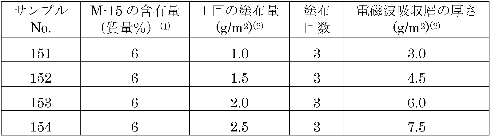
- Example 15 From the amount of flaky graphene fine particles (“M-15” manufactured by XG Sciences, average diameter: 15 ⁇ m, average thickness: 6 to 8 nm) of the amount shown in Table 10, 1.8% by mass of PMMA, and the remaining methyl ethyl ketone An electromagnetic wave absorbing layer 12 made of graphene fine particles / PMMA having a thickness shown in Table 10 was formed in the same manner as in Example 1 except that the dispersion liquid was used. Thus, an electromagnetic wave absorbing film 1 of Example 15 was obtained. Table 10 shows the surface resistance and average light transmittance of the electromagnetic wave absorbing layer 12 of each sample of Example 15 measured in the same manner as Example 1. As is clear from Table 10, in the electromagnetic wave absorbing layer 12 of Example 15, the graphene fine particles were sufficiently uniformly dispersed regardless of the thickness.
- the electromagnetic wave absorbing layer 12 of each electromagnetic wave absorbing film 1 of Example 15 was thermally laminated with the same protective film 1 ′ as in Example 1 to obtain an electromagnetic wave absorbing film laminate 1 ′′ of Example 15. Each electromagnetic wave absorbing film laminate.
- the power of the reflected wave S 11 at a frequency of 1 to 6 GHz of the body 1 ′′ was measured in the same manner as in Example 1 and averaged. Table 10 shows the relationship between the average S 11 and the thickness of the electromagnetic wave absorbing layer 12.
- Example 16 It consists of flaky graphene fine particles (“H-15” manufactured by XG Sciences, average diameter: 15 ⁇ m, average thickness: about 15 nm) in the amount shown in Table 11, 1.8% by mass of PMMA, and the remaining methyl ethyl ketone.
- An electromagnetic wave absorbing layer 12 made of graphene fine particles / PMMA having a thickness shown in Table 11 was formed in the same manner as in Example 1 except that the dispersion was used, and the electromagnetic wave absorbing film 1 of Example 16 was obtained.
- Table 11 shows the surface resistance and average light transmittance of the electromagnetic wave absorbing layer 12 of each sample of Example 16 measured in the same manner as Example 1. As is apparent from Table 11, in the electromagnetic wave absorbing layer 12 of Example 16, the graphene fine particles were sufficiently uniformly dispersed regardless of the thickness.
- the electromagnetic wave absorbing layer 12 of each electromagnetic wave absorbing film 1 of Example 16 was thermally laminated with the same protective film 1 ′ as in Example 1 to obtain an electromagnetic wave absorbing film laminate 1 ′′ of Example 16. Each electromagnetic wave absorbing film laminate.
- the power of the reflected wave S 11 at a frequency of 1 to 6 GHz of the body 1 ′′ was measured in the same manner as in Example 1 and averaged. Table 11 shows the relationship between the average S 11 and the thickness of the electromagnetic wave absorption layer 12.
- Comparative Example 1 The same dispersion as in Example 3 was applied to the plastic film 11 at a thickness of 10.5 g / m 2 (expressed by the weight of graphene fine particles per 1 m 2 ) and dried at 50 ° C. for 5 minutes. An electromagnetic wave absorbing film 1 was produced. The surface resistance of the electromagnetic wave absorbing layer 12 of the electromagnetic wave absorbing film 1 was 3000 ⁇ / ⁇ or more, and the average light transmittance was as high as 20%. From this, it can be seen that when the dispersion is applied once to a predetermined thickness, the thickness unevenness increases and the electromagnetic wave absorbing layer 12 in which the graphene fine particles are aggregated is formed.
- a scanning electron micrograph of a test piece arbitrarily cut out from the electromagnetic wave absorbing film 1 was taken, and the surface roughness was measured with a scanning electron microscope.
- a scanning electron micrograph showing the dispersion state of the graphene fine particles is shown in FIG. 24, and the surface roughness is shown in FIG.
- the graphene fine particles are aggregated, and there are many regions where the graphene fine particles are not present.
- the surface roughness of the electromagnetic wave absorbing layer 12 of Comparative Example 1 was very large, and the thickness unevenness was about 26 ⁇ m.
- Comparative Example 2 An electromagnetic wave absorbing layer 12 was obtained in the same manner as in Example 1 except that the concentration of the graphene fine particles in the dispersion was 12% by mass.
- the surface resistance of the electromagnetic wave absorbing layer 12 was 500 ⁇ / ⁇ or more, and the average light transmittance was as large as 10%. From this, it can be seen that if the concentration of the graphene fine particles in the dispersion liquid is too high, the thickness unevenness becomes large even when applied in three steps, and the electromagnetic wave absorbing layer 12 in which the graphene fine particles are aggregated is formed.
- Comparative Example 3 An electromagnetic wave absorbing layer 12 was obtained in the same manner as in Example 1 except that the concentration of graphene fine particles in the dispersion was 3% by mass and the concentration of PMMA was 5% by mass.
- the surface resistance of the electromagnetic wave absorbing layer 12 was as large as 5000 ⁇ / ⁇ or more. From this, it can be seen that when the mass ratio of PMMA (binder resin) to the graphene fine particles in the dispersion is too large, the surface resistance becomes too large.
Landscapes
- Chemical & Material Sciences (AREA)
- Engineering & Computer Science (AREA)
- Organic Chemistry (AREA)
- Life Sciences & Earth Sciences (AREA)
- Materials Engineering (AREA)
- Wood Science & Technology (AREA)
- Computer Networks & Wireless Communication (AREA)
- Signal Processing (AREA)
- Textile Engineering (AREA)
- Physics & Mathematics (AREA)
- Electromagnetism (AREA)
- Microelectronics & Electronic Packaging (AREA)
- Inorganic Chemistry (AREA)
- Nanotechnology (AREA)
- Shielding Devices Or Components To Electric Or Magnetic Fields (AREA)
- Laminated Bodies (AREA)
- Carbon And Carbon Compounds (AREA)
Abstract
Description
図1に示すように、本発明の電磁波吸収フィルム1はプラスチックフィルム11と、その一面に形成された電磁波吸収層12とからなる。
プラスチックフィルム11を形成する樹脂は、絶縁性とともに十分な強度、可撓性及び加工性を有する限り特に制限されず、例えばポリエステル(ポリエチレンテレフタレート等)、ポリアリーレンサルファイド(ポリフェニレンサルファイド等)、ポリエーテルサルフォン、ポリエーテルエーテルケトン、ポリカーボネート、アクリル樹脂、ポリアミド、ポリイミド、ポリスチレン、ポリオレフィン(ポリエチレン、ポリプロピレン等)等が挙げられる。プラスチックフィルム10の厚さは10~50μm程度で良い。
電磁波吸収層12は、バインダ樹脂により結合されたグラフェン微粒子からなる。
図2に示すように、薄片状のグラフェン微粒子31はベンゼン環が二次元的に連結した板状の構造を有し、単層又は多層のいずれでも良いが、導電性の観点から多層の方が好ましい。グラフェン微粒子31は六角状の格子構造を有するので、各炭素原子は3つの炭素原子に結合し、化学結合に用いられる4つの外殻電子のうちの1つは自由な状態にある(自由電子となる)。自由電子は結晶格子に沿って移動できるので、グラフェン微粒子31は高い導電性を有する。
本発明に使用するバインダ樹脂は、有機溶媒に可溶でグラフェン微粒子を均一に分散できるものであれば特に限定されず、熱可塑性樹脂でも熱硬化性樹脂(光硬化性樹脂)でも良い。本発明に使用し得る熱可塑性樹脂としては、ポリメチルアクリレート、ポリメチルメタクリレート等のアクリル樹脂、ポリスチレン、ポリカーボネート、ポリ塩化ビニル、ABS樹脂等が挙げられるが、なかでもポリメチルメタクリレート及びポリスチレンが好ましい。本発明に使用し得る熱硬化性樹脂としては、エポキシ樹脂、フェノール樹脂、不飽和ポリエステル樹脂、アルキッド樹脂、ポリウレタン等が挙げられる。また本発明に使用し得る光硬化性樹脂としては、ジアクリレート類、トリアクリレート類等が挙げられる。熱硬化性樹脂及び光硬化性樹脂の場合、オリゴマーの状態で有機溶媒に溶解するのが好ましい。
バインダ樹脂/グラフェン微粒子の質量比が小さい程、電磁波吸収層は高い電磁波吸収能を発揮する。しかし、バインダ樹脂の割合が低すぎるとグラフェン微粒子の剥落が起こり易くなる。従って、良好な電磁波吸収能と高いグラフェン微粒子密着性を両立させるために、バインダ樹脂/グラフェン微粒子の質量比は1以下が好ましく、0.5以下がより好ましい。バインダ樹脂/グラフェン微粒子の質量比の下限は0.05が好ましく、0.1がより好ましく、0.3が最も好ましい。
電磁波吸収層におけるグラフェン微粒子の分布が均一でないと、(a) グラフェン微粒子の凝集によりグラフェン微粒子が不十分な領域が発生し、電磁波吸収フィルムは所望の表面抵抗を有さず、もって十分な電磁波吸収能を発揮しないだけでなく、(b) 個々の電子機器又は部品に応じて電磁波吸収フィルムを分割して使用する場合、グラフェン微粒子が不十分な領域が多いために所望の電磁波吸収能を発揮しない分割片ができるという問題も発生する。電磁波吸収層におけるグラフェン微粒子の分布は、(1) 電磁波吸収層の顕微鏡写真から求めたグラフェン微粒子が存在しない領域の面積率、(2) 電磁波吸収層の表面粗さ、及び(3) 電磁波吸収層の光透過率により評価することができる。
図4に示すように、グラフェン微粒子の凝集が起こった電磁波吸収層12では、グラフェン微粒子の凝集域33と、グラフェン微粒子が存在しない領域34とがある。これは電子顕微鏡写真により容易に確認できる。グラフェン微粒子の凝集域33の面積をS1とし、グラフェン微粒子が存在しない領域の面積をS2とすると、グラフェン微粒子が存在しない領域の面積率RsはS2/(S1+S2)×100(%)により求めることができる。電磁波吸収層12の任意の3つの視野の電子顕微鏡写真(倍率:500倍、サイズ:10 cm×10 cm)における面積率Rsを平均することにより、グラフェン微粒子が存在しない領域の面積率を求める。この面積率が5%以内であれば、グラフェン微粒子の分散は良好であると言える。グラフェン微粒子が存在しない領域の面積率は好ましくは2%以内であり、より好ましくは0%である。
電磁波吸収層ではグラフェン微粒子がバインダ樹脂より多いので、グラフェン微粒子が凝集した部分はグラフェン微粒子が少ない部分より厚くなる。そのため、グラフェン微粒子の分布の均一度は、電磁波吸収層の厚さ分布を測定することにより求めることができる。
グラフェン微粒子の分布の均一性は電磁波吸収フィルム1の光透過率により求めることもできる。グラフェン微粒子が完全に均一に分散している場合、全体の光透過率は0%であるが、グラフェン微粒子に凝集がある場合、グラフェン微粒子が少ない部分又は全くない部分は光が透過するので、全体の光透過率は上昇する。そこで、光透過率を比較することによりグラフェン微粒子の凝集度を評価することができる。なお、光透過率の測定は、電磁波吸収フィルム1から任意に切り出した複数の試験片に対して行い、測定値を平均する。
十分な電磁波吸収能を発揮するために、電磁波吸収層12の表面抵抗は好ましくは50~250Ω/□であり、より好ましくは100~200Ω/□である。表面抵抗は、10 cm×10 cmの電磁波吸収フィルム1の正方形試験片に対して直流二端子法により測定する。一般に、グラフェン微粒子の分布が均一であると電磁波吸収層12の表面抵抗は小さくなる。
電磁波吸収層12の表面抵抗は単位面積当たりのグラフェン微粒子の量に依存し、グラフェン微粒子の量により電磁波吸収層12の厚さが決まる。そこで、上記所望の表面抵抗を有する電磁波吸収層12の厚さをグラフェン微粒子の単位面積当たりの量により表すことにする。グラフェン微粒子の単位面積当たりの量で表した電磁波吸収層12の厚さは好ましくは2~15 g/m2であり、より好ましくは3~12 g/m2であり、最も好ましく 4~8 g/m2である。
グラフェン微粒子の脱落を防止するために電磁波吸収層12の上に保護フィルムを形成するのが好ましい。保護フィルム自体は電磁波吸収フィルム1を構成するプラスチックフィルムと同じポリマーからなるもので良い。保護フィルムの接着は接着剤により行うことができるが、接着の簡単化のために熱融着が好ましい。図8(a) に示す例では、保護フィルム1’はプラスチックフィルム11’に熱融着層13’を形成してなるものである。なお、保護フィルム1’との密着性を向上させるために、電磁波吸収フィルム1のプラスチックフィルム11にも熱融着層13を設けるのが好ましい。保護フィルム1’の熱融着層13’を電磁波吸収層12に熱融着させることにより、保護フィルム1’は電磁波吸収フィルム1に密着し、電磁波吸収層12が保護された電磁波吸収フィルム積層体1”となる。各熱融着層13,13’はエチレン・α-オレフィン共重合体のような低融点のポリエチレン等により形成することができる。
(1) グラフェン微粒子の分散液の調製
グラフェン微粒子、バインダ樹脂及び有機溶媒を含有する分散液は、グラフェン微粒子の有機溶媒分散液にバインダ樹脂の有機溶媒溶液を混合することにより調製するのが好ましい。これは、グラフェン微粒子が凝集し易いため、グラフェン微粒子及びバインダ樹脂を同時に有機溶媒に混合すると、グラフェン微粒子が凝集してしまうおそれがあるためである。両溶液を混合することにより得られるグラフェン微粒子の分散液において、グラフェン微粒子の濃度は1~10質量%が好ましく、1~8質量%がより好ましく、2~8質量%が最も好ましく、特に2~7質量%が好ましい。また、バインダ樹脂/グラフェン微粒子の質量比は0.05~1が好ましく、0.05~0.5がより好ましく、0.1~0.5が最も好ましい。
所望の濃度の分散液をプラスチックフィルム11に一回で塗布すると、図9に概略的に示すように、分散液3中のグラフェン微粒子31が乾燥過程で凝集してしまうことが分った。これは、分散液3中ではグラフェン微粒子31の濃度は比較的低いので、凝集は起こらないが、乾燥過程で有機溶媒32の割合が低下していくと、グラフェン微粒子32の濃度が上昇し、凝集し易くなるためであると考えられる。図9において、33はグラフェン微粒子32が凝集した領域を示す。
図13(a) 及び図13(b) に示すように、50ΩのマイクロストリップラインMSL(64.4 mm×4.4 mm)と、マイクロストリップラインMSLを支持する絶縁基板50と、絶縁基板50の下面に接合された接地グランド電極51と、マイクロストリップラインMSLの両端に接続された導電性ピン52,52と、ネットワークアナライザNAと、ネットワークアナライザNAを導電性ピン52,52に接続する同軸ケーブル53,53とで構成されたシステムを用い、マイクロストリップラインMSLに電磁波吸収フィルムの試験片TP2を粘着剤により貼付し、0.1~6 GHzの入射波に対して、反射波S11の電力及び透過波S12の電力を測定する。入射した電力Pinから反射波S11の電力及び透過波S12の電力を差し引くことにより、電力損失Plossを求め、Plossを入射電力Pinで割ることによりノイズ吸収率Ploss/Pinを求める。
表1に示す量の薄片状のグラフェン微粒子(XG Sciences社製の「M-25」、平均径:25μm、平均厚さ:約6~8 nm)と、グラフェン微粒子の1/2の量のポリメチルメタクリレート(PMMA)と、残部キシレン/イソプロピルアルコールの混合溶媒(質量比:60/40)とからなる各分散液を、厚さ16μmのポリエチレンテレフタレート(PET)フィルム11に塗布し、50℃で5分間乾燥させて、表1に示す厚さのグラフェン微粒子/PMMA層を形成した。各グラフェン微粒子/PMMA層に対してこの手順を合計3回繰り返し、表1に示す厚さのグラフェン微粒子/PMMAからなる電磁波吸収層12を形成し、電磁波吸収フィルム1を得た。直流二端子法により測定した電磁波吸収層12の表面抵抗を表1に示す。
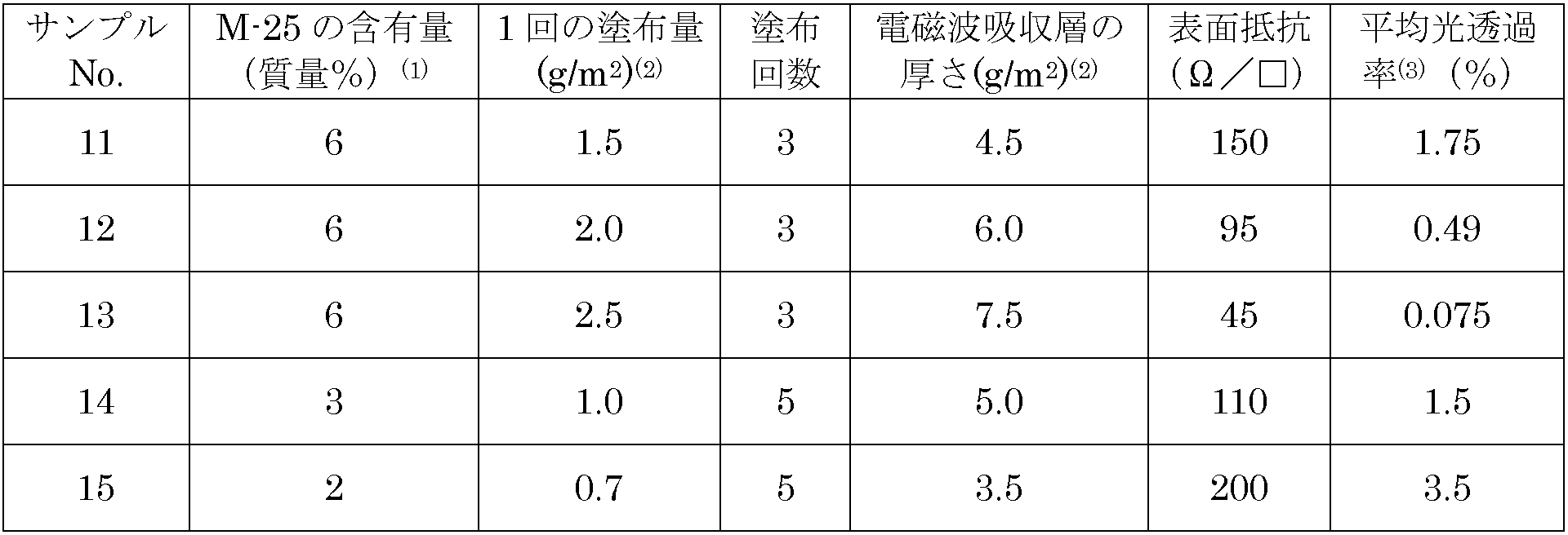
(2) 1 m2当たりのグラフェン微粒子のグラム数で表す。
(3) プラスチックフィルムの光透過率を100%としたときの平均光透過率(%)。
実施例1の各電磁波吸収フィルム積層体1”の試験片TP2に対して、150℃の温度及び200 kg/cm2の圧力で熱加圧を行い、実施例2の試験片TP2とした。実施例1と同様にして実施例2の試験片TP2の1~6 GHzの周波数における反射波S11の電力を実施例1と同様に測定し、平均した。平均S11と電磁波吸収層12の厚さとの関係を図14に示す。図14から明らかなように、熱加圧によりS11は改善された。
薄片状のグラフェン微粒子をXG Sciences社製の「H-5」(平均径:5μm、平均厚さ:約15 nm)に変更した以外実施例1と同様にして、表2に示す厚さのグラフェン微粒子/PMMAからなる電磁波吸収層12を形成し、電磁波吸収フィルム1を得た。実施例1と同様に測定した電磁波吸収層12の表面抵抗及び平均光透過率を表2に示す。表2から明らかなように、実施例3の電磁波吸収層12では厚さに関係なくグラフェン微粒子が十分に均一に分散していた。

(2) 1 m2当たりのグラフェン微粒子のグラム数で表す。
(3) プラスチックフィルムの光透過率を100%としたときの平均光透過率(%)。
実施例3の各サンプルの試験片TP2に対して、150℃の温度及び200 kg/cm2の圧力で熱加圧を行い、実施例4の試験片TP2とした。実施例1と同様にして実施例4の各サンプルの試験片TP2の1~6 GHzの周波数における反射波S11の電力を実施例1と同様に測定し、平均した。平均S11と電磁波吸収層12の厚さとの関係を図18に示す。図18から明らかなように、熱加圧によりS11は改善された。
表3に示す量の薄片状のグラフェン微粒子(XG Sciences社製の「H-25」、平均径:25μm、平均厚さ:約15 nm)と、3質量%のPMMAと、残部キシレン/イソプロピルアルコールの混合溶媒(質量比:60/40)とからなる分散液を用いた以外、実施例1と同様にして表3に示す厚さのグラフェン微粒子/PMMAからなる電磁波吸収層12を形成し、実施例5の電磁波吸収フィルム1を得た。実施例1と同様に測定した実施例5の各サンプルの電磁波吸収層12の表面抵抗及び平均光透過率を表3に示す。表3から明らかなように、実施例5の電磁波吸収層12では厚さに関係なくグラフェン微粒子が十分に均一に分散していた。
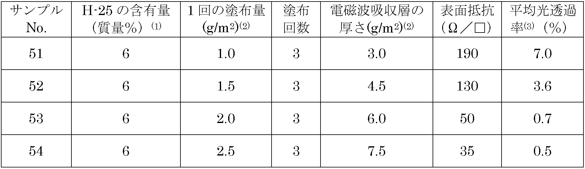
(2) 1 m2当たりのグラフェン微粒子のグラム数で表す。
(3) プラスチックフィルムの光透過率を100%としたときの平均光透過率(%)。
表4に示す量の薄片状のグラフェン微粒子(XG Sciences社製の「H-25」、平均径:25μm、平均厚さ:約15 nm)と、1.8質量%のPMMAと、残部キシレン/イソプロピルアルコールの混合溶媒(質量比:60/40)とからなる分散液を用いた以外、実施例1と同様にして表4に示す厚さのグラフェン微粒子/PMMAからなる電磁波吸収層12を形成し、実施例6の電磁波吸収フィルム1を得た。実施例1と同様に測定した実施例6の各サンプルの電磁波吸収層12の表面抵抗及び平均光透過率を表4に示す。表4から明らかなように、実施例6の電磁波吸収層12では厚さに関係なくグラフェン微粒子が十分に均一に分散していた。
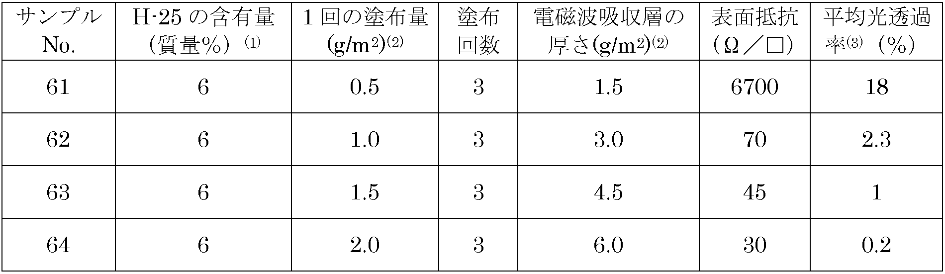
(2) 1 m2当たりのグラフェン微粒子のグラム数で表す。
(3) プラスチックフィルムの光透過率を100%としたときの平均光透過率(%)。
実施例6の各サンプルの試験片TP2に対して、150℃の温度及び200 kg/cm2の圧力で熱加圧を行い、実施例7の試験片TP2とした。実施例1と同様にして実施例7の各サンプルの試験片TP2の1~6 GHzの周波数における反射波S11の電力を実施例1と同様に測定し、平均した。平均S11と電磁波吸収層12の厚さとの関係を図20に示す。図19から明らかなように、熱加圧によりS11は改善された。
表5に示す量の薄片状のグラフェン微粒子(XG Sciences社製の「H-25」、平均径:25μm、平均厚さ:約15 nm)と、1.2質量%のPMMAと、残部メチルエチルケトンとからなる分散液を用いた以外、実施例1と同様にして表5に示す厚さのグラフェン微粒子/PMMAからなる電磁波吸収層12を形成し、実施例8の電磁波吸収フィルム1を得た。実施例1と同様に測定した実施例8の各サンプルの電磁波吸収層12の表面抵抗及び平均光透過率を表5に示す。表5から明らかなように、実施例8の電磁波吸収層12では厚さに関係なくグラフェン微粒子が十分に均一に分散していた。

(2) 1 m2当たりのグラフェン微粒子のグラム数で表す。
(3) プラスチックフィルムの光透過率を100%としたときの平均光透過率(%)。
表6に示す量の薄片状のグラフェン微粒子(XG Sciences社製の「H-25」、平均径:25μm、平均厚さ:約15 nm)と、1.8質量%のPMMAと、残部メチルエチルケトンとからなる分散液を用いた以外、実施例1と同様にして表6に示す厚さのグラフェン微粒子/PMMAからなる電磁波吸収層12を形成し、実施例9の電磁波吸収フィルム1を得た。実施例1と同様に測定した実施例9の各サンプルの電磁波吸収層12の表面抵抗及び平均光透過率を表6に示す。表6から明らかなように、実施例9の電磁波吸収層12では厚さに関係なくグラフェン微粒子が十分に均一に分散していた。
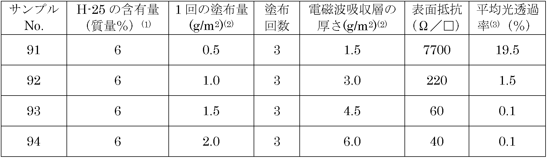
(2) 1 m2当たりのグラフェン微粒子のグラム数で表す。
(3) プラスチックフィルムの光透過率を100%としたときの平均光透過率(%)。
表7に示す量の薄片状のグラフェン微粒子(XG Sciences社製の「H-25」、平均径:25μm、平均厚さ:約15 nm)と、0.6質量%のPMMAと、残部メチルエチルケトンとからなる分散液を用いた以外、実施例1と同様にして表7に示す厚さのグラフェン微粒子/PMMAからなる電磁波吸収層12を形成し、実施例10の電磁波吸収フィルム1を得た。実施例1と同様に測定した実施例10の各サンプルの電磁波吸収層12の表面抵抗及び平均光透過率を表7に示す。表7から明らかなように、実施例10の電磁波吸収層12では厚さに関係なくグラフェン微粒子が十分に均一に分散していた。
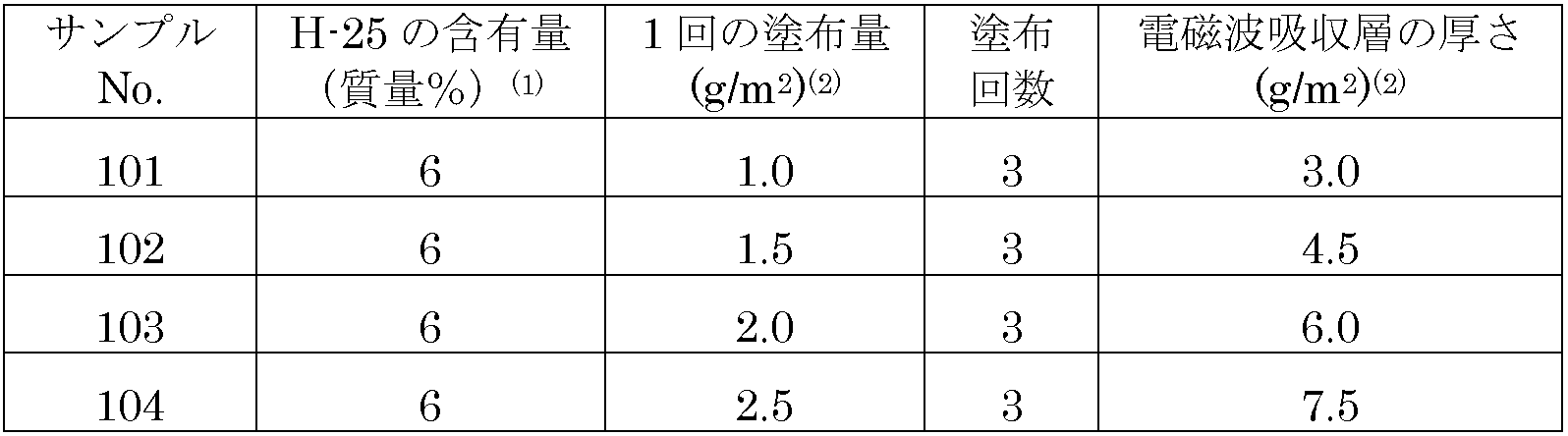
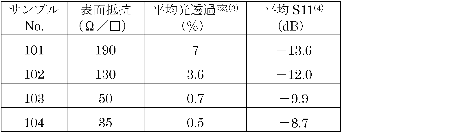
(2) 1 m2当たりのグラフェン微粒子のグラム数で表す。
(3) プラスチックフィルムの光透過率を100%としたときの平均光透過率(%)。
(4) 1~6 GHzの周波数におけるS11の平均。
表8に示す量の薄片状のグラフェン微粒子(XG Sciences社製の「H-25」、平均径:25μm、平均厚さ:約15 nm)と、1.8質量%のポリビニルアルコール(PVA)と、残部キシレン/イソプロピルアルコールの混合溶媒(質量比:60/40)とからなる分散液を用いた以外、実施例1と同様にして表8に示す厚さのグラフェン微粒子/PMMAからなる電磁波吸収層12を形成し、実施例11の電磁波吸収フィルム1を得た。実施例1と同様に測定した実施例11の各サンプルの電磁波吸収層12の表面抵抗及び平均光透過率を表7に示す。表8から明らかなように、実施例11の電磁波吸収層12では、グラフェン微粒子が十分に均一に分散していることが分かる。
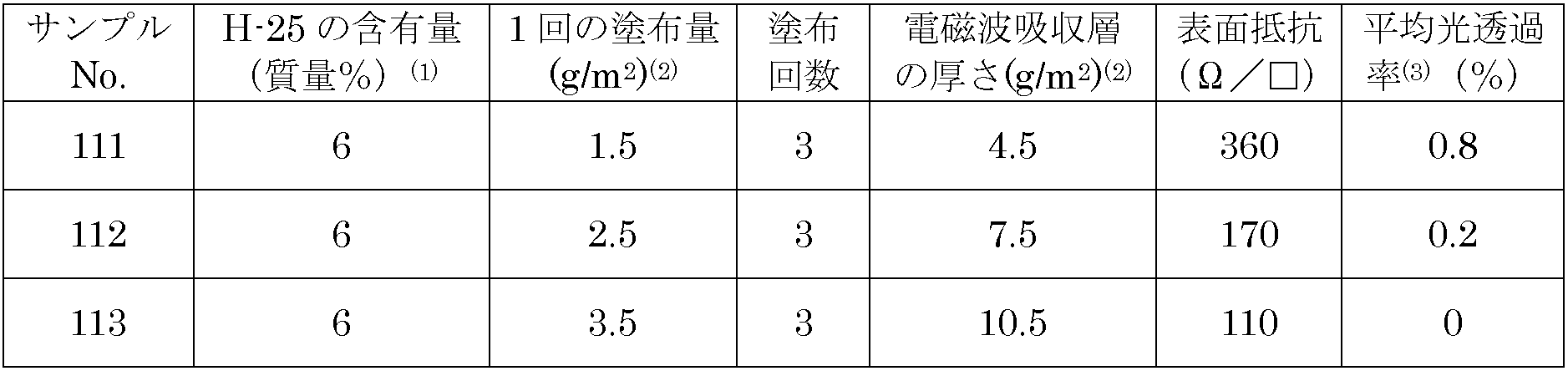
(2) 1 m2当たりのグラフェン微粒子のグラム数で表す。
(3) プラスチックフィルムの光透過率を100%としたときの平均光透過率(%)。
実施例11の各サンプルの試験片TP2に対して、150℃の温度及び200 kg/cm2の圧力で熱加圧を行い、実施例12の試験片TP2とした。実施例1と同様にして実施例12の各サンプルの試験片TP2の1~6 GHzの周波数における反射波S11の電力を実施例1と同様に測定し、平均した。平均S11と電磁波吸収層12の厚さとの関係を図21に示す。図21から明らかなように、熱加圧によりS11は改善された。
表9に示す量の薄片状のグラフェン微粒子(XG Sciences社製の「M-5」、平均径:5μm、平均厚さ:約6~8 nm)と、3質量%のPMMAと、残部キシレン/イソプロピルアルコールの混合溶媒(質量比:60/40)とからなる分散液を用いた以外、実施例1と同様にして表9に示す厚さのグラフェン微粒子/PMMAからなる電磁波吸収層12を形成し、実施例13の電磁波吸収フィルム1を得た。実施例1と同様に測定した実施例13の各サンプルの電磁波吸収層12の表面抵抗及び平均光透過率を表9に示す。表9から明らかなように、実施例13の電磁波吸収層12では、グラフェン微粒子が十分に均一に分散していることが分かる。
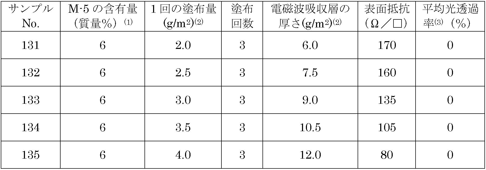
(2) 1 m2当たりのグラフェン微粒子のグラム数で表す。
(3) プラスチックフィルムの光透過率を100%としたときの平均光透過率(%)。
実施例14の各サンプルの試験片TP2に対して、150℃の温度及び200 kg/cm2の圧力で熱加圧を行い、実施例14の試験片TP2とした。実施例1と同様にして実施例14の各サンプルの試験片TP2の1~6 GHzの周波数における反射波S11の電力を実施例1と同様に測定し、平均した。平均S11と電磁波吸収層12の厚さとの関係を図23に示す。図23から明らかなように、熱加圧によりS11は改善された。
表10に示す量の薄片状のグラフェン微粒子(XG Sciences社製の「M-15」、平均径:15μm、平均厚さ:6~8 nm)と、1.8質量%のPMMAと、残部メチルエチルケトンとからなる分散液を用いた以外、実施例1と同様にして表10に示す厚さのグラフェン微粒子/PMMAからなる電磁波吸収層12を形成し、実施例15の電磁波吸収フィルム1を得た。実施例1と同様に測定した実施例15の各サンプルの電磁波吸収層12の表面抵抗及び平均光透過率を表10に示す。表10から明らかなように、実施例15の電磁波吸収層12では厚さに関係なくグラフェン微粒子が十分に均一に分散していた。
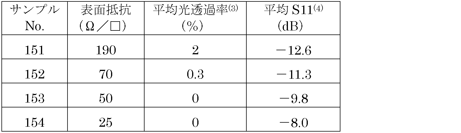
(2) 1 m2当たりのグラフェン微粒子のグラム数で表す。
(3) プラスチックフィルムの光透過率を100%としたときの平均光透過率(%)。
(4) 1~6 GHzの周波数におけるS11の平均。
表11に示す量の薄片状のグラフェン微粒子(XG Sciences社製の「H-15」、平均径:15μm、平均厚さ:約15 nm)と、1.8質量%のPMMAと、残部メチルエチルケトンとからなる分散液を用いた以外、実施例1と同様にして表11に示す厚さのグラフェン微粒子/PMMAからなる電磁波吸収層12を形成し、実施例16の電磁波吸収フィルム1を得た。実施例1と同様に測定した実施例16の各サンプルの電磁波吸収層12の表面抵抗及び平均光透過率を表11に示す。表11から明らかなように、実施例16の電磁波吸収層12では厚さに関係なくグラフェン微粒子が十分に均一に分散していた。
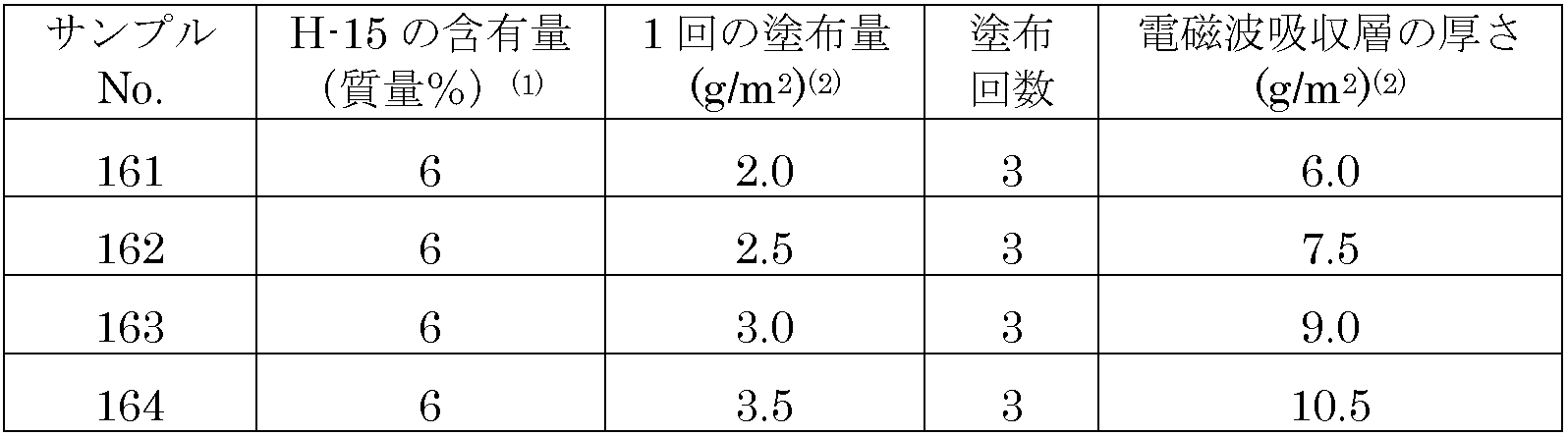

(2) 1 m2当たりのグラフェン微粒子のグラム数で表す。
(3) プラスチックフィルムの光透過率を100%としたときの平均光透過率(%)。
(4) 1~6 GHzの周波数におけるS11の平均。
実施例3と同じ分散液を10.5 g/m2(1 m2当たりのグラフェン微粒子の重量で表す。)の厚さに1回でプラスチックフィルム11に塗布し、50℃で5分間乾燥させて、電磁波吸収フィルム1を作製した。この電磁波吸収フィルム1の電磁波吸収層12の表面抵抗は3000Ω/□以上であり、平均光透過率は 20%と大きかった。これから、分散液を所定の厚さに1回で塗布すると、厚さムラが大きくなり、グラフェン微粒子が凝集した電磁波吸収層12が形成されることが分かる。
分散液中のグラフェン微粒子の濃度を12質量%とした以外実施例1と同様にして電磁波吸収層12を得た。電磁波吸収層12の表面抵抗は500Ω/□以上であり、平均光透過率は10%と大きかった。これから、分散液中のグラフェン微粒子の濃度が高すぎると、3回に分けて塗布しても厚さムラが大きくなり、グラフェン微粒子が凝集した電磁波吸収層12が形成されることが分かる。
分散液中のグラフェン微粒子の濃度を3質量%とし、PMMAの濃度を5質量%とした以外実施例1と同様にして電磁波吸収層12を得た。電磁波吸収層12の表面抵抗は5000Ω/□以上と大きかった。これから、分散液中でグラフェン微粒子に対するPMMA(バインダ樹脂)の質量比が大きすぎると、表面抵抗が大きくなり過ぎることが分かる。
Claims (11)
- プラスチックフィルムの一面に、薄片状のグラフェン微粒子及びバインダ樹脂を含有する電磁波吸収層を形成してなる電磁波吸収フィルムであって、前記電磁波吸収層の厚さが2~15 g/m2(1 m2当たりのグラフェン微粒子の重量で表す。)であり、前記電磁波吸収層におけるバインダ樹脂とグラフェン微粒子との質量比が0.05~0.5であり、かつ前記電磁波吸収層において前記グラフェン微粒子が存在しない領域の合計面積率が5%以下であることを特徴とする電磁波吸収フィルム。
- 請求項1に記載の電磁波吸収フィルムにおいて、前記グラフェン微粒子が5~100μmの平均径及び5~50 nmの平均厚さを有することを特徴とする電磁波吸収フィルム。
- 請求項1又は2に記載の電磁波吸収フィルムにおいて、前記バインダ樹脂がアクリル樹脂、ポリスチレン樹脂又はポリビニルアルコールであることを特徴とする電磁波吸収フィルム。
- 請求項1~3のいずれかに記載の電磁波吸収フィルムにおいて、前記電磁波吸収層の表面に保護フィルムが積層されていることを特徴とする電磁波吸収フィルム。
- 請求項1~4のいずれかに記載の電磁波吸収フィルムを製造する方法において、1~10質量%のグラフェン微粒子及び0.05~5質量%のバインダ樹脂を含有する有機溶媒分散液をプラスチックフィルムの一面に塗布した後乾燥する工程を複数回繰り返すことを特徴とする方法。
- 請求項5に記載の電磁波吸収フィルムの製造方法において、前記分散液における前記バインダ樹脂と前記グラフェン微粒子との質量比が0.05~1であることを特徴とする方法。
- 請求項5又は6に記載の電磁波吸収フィルムの製造方法において、前記分散液の一回の塗布量を1~3.5 g/m2(1 m2当たりのグラフェン微粒子の重量で表す。)とすることを特徴とする方法。
- 請求項5~7のいずれかに記載の電磁波吸収フィルムの製造方法において、前記有機溶媒がケトン類、芳香族炭化水素類及びアルコール類からなる群から選ばれた少なくとも一種であることを特徴とする方法。
- 請求項5~8のいずれかに記載の電磁波吸収フィルムの製造方法において、前記分散液の塗布をスプレー法により行うことを特徴とする方法。
- 請求項5~9のいずれかに記載の電磁波吸収フィルムの製造方法において、前記乾燥工程を30~100℃に加熱することにより行うことを特徴とする方法。
- 請求項5~10のいずれかに記載の電磁波吸収フィルムの製造方法において、前記分散液の塗布・乾燥工程を2~6回繰り返すことを特徴とする方法。
Priority Applications (4)
| Application Number | Priority Date | Filing Date | Title |
|---|---|---|---|
| EP13857629.3A EP2925108B1 (en) | 2012-11-20 | 2013-11-05 | Electromagnetic wave absorption film and its production method for manufacturing same |
| CN201380060055.5A CN104798453B (zh) | 2012-11-20 | 2013-11-05 | 电磁波吸收膜及其制造方法 |
| US14/439,115 US9550206B2 (en) | 2012-11-20 | 2013-11-05 | Electromagnetic-wave-absorbing film and its production method |
| KR1020157016218A KR102031611B1 (ko) | 2012-11-20 | 2013-11-05 | 전자파 흡수 필름 및 그 제조 방법 |
Applications Claiming Priority (2)
| Application Number | Priority Date | Filing Date | Title |
|---|---|---|---|
| JP2012254779A JP5426002B1 (ja) | 2012-11-20 | 2012-11-20 | 電磁波吸収フィルムの製造方法 |
| JP2012-254779 | 2012-11-20 |
Publications (1)
| Publication Number | Publication Date |
|---|---|
| WO2014080754A1 true WO2014080754A1 (ja) | 2014-05-30 |
Family
ID=50287319
Family Applications (1)
| Application Number | Title | Priority Date | Filing Date |
|---|---|---|---|
| PCT/JP2013/079863 Ceased WO2014080754A1 (ja) | 2012-11-20 | 2013-11-05 | 電磁波吸収フィルム及びその製造方法 |
Country Status (7)
| Country | Link |
|---|---|
| US (1) | US9550206B2 (ja) |
| EP (1) | EP2925108B1 (ja) |
| JP (1) | JP5426002B1 (ja) |
| KR (1) | KR102031611B1 (ja) |
| CN (1) | CN104798453B (ja) |
| TW (1) | TWI607688B (ja) |
| WO (1) | WO2014080754A1 (ja) |
Families Citing this family (23)
| Publication number | Priority date | Publication date | Assignee | Title |
|---|---|---|---|---|
| JP5674986B1 (ja) * | 2013-08-12 | 2015-02-25 | 加川 清二 | 放熱フィルム、並びにその製造方法及び装置 |
| JP6402584B2 (ja) * | 2014-10-23 | 2018-10-10 | 住友ベークライト株式会社 | 電磁波シールド用フィルムの製造方法 |
| JP6402612B2 (ja) * | 2014-12-12 | 2018-10-10 | 住友ベークライト株式会社 | 電磁波シールド用フィルムの製造方法 |
| TWI631889B (zh) * | 2014-12-27 | 2018-08-01 | 中原大學 | Electromagnetic wave shielding composite film |
| CN104735964B (zh) * | 2015-02-02 | 2018-04-27 | 邓秀梅 | 微波暗室用吸波材料及其印制法生产方法 |
| KR102049574B1 (ko) * | 2015-10-30 | 2019-11-27 | 주식회사 엘지화학 | 자성 산화철-그래핀 복합체의 제조 방법 |
| JP6863099B2 (ja) * | 2016-06-06 | 2021-04-21 | 東レ株式会社 | グラフェン/有機溶媒分散液、グラフェン−活物質複合体粒子の製造方法および電極ペーストの製造方法 |
| CN106850906B (zh) * | 2016-07-21 | 2019-10-08 | 济南圣泉集团股份有限公司 | 生物质石墨烯在无线通讯设备壳体中的应用 |
| WO2018066574A1 (ja) * | 2016-10-04 | 2018-04-12 | 日本ゼオン株式会社 | 電磁波シールド構造体およびその製造方法 |
| CN106519816B (zh) * | 2016-10-08 | 2018-09-11 | 江苏大使同丰涂料有限公司 | 一种吸收电磁波的涂料及其制备方法与用途 |
| TWI629485B (zh) * | 2017-05-19 | 2018-07-11 | 中華精測科技股份有限公司 | 用於探針卡之探針及其製造方法 |
| CN109082072B (zh) * | 2017-06-13 | 2021-02-23 | 中国科学院苏州纳米技术与纳米仿生研究所 | 石墨烯/环氧树脂复合吸波材料及其制备方法和应用 |
| CN107383408A (zh) * | 2017-07-19 | 2017-11-24 | 刘世德 | 电磁波吸收材料的制备方法 |
| US11202398B2 (en) | 2017-09-28 | 2021-12-14 | Murata Manufacturing Co., Ltd. | Electromagnetic shielding material and method for producing the same |
| TWI708801B (zh) * | 2018-02-26 | 2020-11-01 | 謙華科技股份有限公司 | 石墨烯複合薄膜的製造方法 |
| WO2019205011A1 (zh) * | 2018-04-25 | 2019-10-31 | 深圳鹏汇功能材料有限公司 | 水性吸波涂料及其制备方法和应用 |
| JP2021523271A (ja) * | 2018-05-09 | 2021-09-02 | ナイアガラ・ボトリング・リミテツド・ライアビリテイー・カンパニー | 改善された分散体に由来するポリ(エチレンテレフタレート)グラフェンナノコンポジット |
| CN109548394B (zh) * | 2018-11-27 | 2020-06-12 | 湖南国盛石墨科技有限公司 | 一种柔性pu石墨烯电磁屏蔽材料及其制备方法 |
| ES2778548A1 (es) * | 2019-11-25 | 2020-08-10 | Santafe Jesus Perez | Dispositivo para neutralizar la transmisión de ondas electromagnéticas por apantallamiento eletromagnético |
| CN111286225A (zh) * | 2020-02-22 | 2020-06-16 | 东莞市鹏威能源科技有限公司 | 一种石墨烯吸波膜涂料及其制备方法和应用 |
| CN111592744A (zh) * | 2020-06-29 | 2020-08-28 | 江西伟普科技有限公司 | 一种金属负载碳/聚合物基电磁屏蔽材料及其制备方法 |
| CN111548618A (zh) * | 2020-06-29 | 2020-08-18 | 江西伟普科技有限公司 | 一种金属负载碳/聚合物基电磁屏蔽材料及其制备方法 |
| CN112659673A (zh) * | 2020-12-18 | 2021-04-16 | 苏州驭奇材料科技有限公司 | 一种具有高导热性的高频电磁波吸收膜及其生产装置 |
Citations (5)
| Publication number | Priority date | Publication date | Assignee | Title |
|---|---|---|---|---|
| JP2006114877A (ja) | 2004-09-15 | 2006-04-27 | Suzuki Sogyo Co Ltd | 電磁波吸収シート、電磁波吸収シート積層体及びそれらを用いた電磁波吸収性ハウジング |
| JP2010153542A (ja) | 2008-12-25 | 2010-07-08 | Ado Union Kenkyusho:Kk | 電磁波抑制シート及びその製造方法 |
| JP2011249614A (ja) * | 2010-05-27 | 2011-12-08 | Nitto Denko Corp | 誘電体シート及びその製造方法、並びに、電磁波吸収体 |
| JP2012151242A (ja) * | 2011-01-18 | 2012-08-09 | Tdk Corp | 電磁ノイズ対策部材及びこれを用いた電磁ノイズ対策方法 |
| JP2012174833A (ja) * | 2011-02-21 | 2012-09-10 | Kj Specialty Paper Co Ltd | 電磁波吸収シート |
Family Cites Families (2)
| Publication number | Priority date | Publication date | Assignee | Title |
|---|---|---|---|---|
| WO2012108371A1 (ja) * | 2011-02-09 | 2012-08-16 | 株式会社インキュベーション・アライアンス | 多層グラフェン被覆基板の製造方法 |
| KR20130104869A (ko) * | 2012-03-15 | 2013-09-25 | 주식회사 동진쎄미켐 | 판상의 그라핀을 포함한 전자파 차폐용 코팅 조성물 |
-
2012
- 2012-11-20 JP JP2012254779A patent/JP5426002B1/ja not_active Expired - Fee Related
-
2013
- 2013-11-05 KR KR1020157016218A patent/KR102031611B1/ko active Active
- 2013-11-05 US US14/439,115 patent/US9550206B2/en active Active
- 2013-11-05 EP EP13857629.3A patent/EP2925108B1/en not_active Not-in-force
- 2013-11-05 WO PCT/JP2013/079863 patent/WO2014080754A1/ja not_active Ceased
- 2013-11-05 CN CN201380060055.5A patent/CN104798453B/zh not_active Expired - Fee Related
- 2013-11-15 TW TW102141577A patent/TWI607688B/zh not_active IP Right Cessation
Patent Citations (5)
| Publication number | Priority date | Publication date | Assignee | Title |
|---|---|---|---|---|
| JP2006114877A (ja) | 2004-09-15 | 2006-04-27 | Suzuki Sogyo Co Ltd | 電磁波吸収シート、電磁波吸収シート積層体及びそれらを用いた電磁波吸収性ハウジング |
| JP2010153542A (ja) | 2008-12-25 | 2010-07-08 | Ado Union Kenkyusho:Kk | 電磁波抑制シート及びその製造方法 |
| JP2011249614A (ja) * | 2010-05-27 | 2011-12-08 | Nitto Denko Corp | 誘電体シート及びその製造方法、並びに、電磁波吸収体 |
| JP2012151242A (ja) * | 2011-01-18 | 2012-08-09 | Tdk Corp | 電磁ノイズ対策部材及びこれを用いた電磁ノイズ対策方法 |
| JP2012174833A (ja) * | 2011-02-21 | 2012-09-10 | Kj Specialty Paper Co Ltd | 電磁波吸収シート |
Non-Patent Citations (1)
| Title |
|---|
| See also references of EP2925108A4 |
Also Published As
| Publication number | Publication date |
|---|---|
| KR20150087351A (ko) | 2015-07-29 |
| US20150259546A1 (en) | 2015-09-17 |
| KR102031611B1 (ko) | 2019-10-14 |
| TW201433254A (zh) | 2014-08-16 |
| TWI607688B (zh) | 2017-12-01 |
| JP2014103283A (ja) | 2014-06-05 |
| EP2925108B1 (en) | 2019-01-02 |
| JP5426002B1 (ja) | 2014-02-26 |
| CN104798453B (zh) | 2018-03-02 |
| US9550206B2 (en) | 2017-01-24 |
| CN104798453A (zh) | 2015-07-22 |
| EP2925108A1 (en) | 2015-09-30 |
| EP2925108A4 (en) | 2016-07-13 |
Similar Documents
| Publication | Publication Date | Title |
|---|---|---|
| JP5426002B1 (ja) | 電磁波吸収フィルムの製造方法 | |
| JP5771275B2 (ja) | 高い放熱性を有する電磁波吸収フィルム | |
| CN103959927B (zh) | 复合电磁波吸收片 | |
| CN101379161B (zh) | 碱性溶液可清洗的抗静电组合物和使用其而制得的聚合物产品 | |
| JP5007777B2 (ja) | 透明導電積層体 | |
| JP5980673B2 (ja) | 放熱フィルム、並びにその製造方法及び装置 | |
| TWI325739B (en) | Electroconductive paste, its manufacturing method, circuit board using the same electroconductive paste, and its manufacturing method | |
| Liu et al. | Highly flexible electromagnetic interference shielding films based on ultrathin Ni/Ag composites on paper substrates | |
| Gnidakouong et al. | Electromagnetic interference shielding behavior of hybrid carbon nanotube/exfoliated graphite nanoplatelet coated glass fiber composites | |
| TWI631889B (zh) | Electromagnetic wave shielding composite film | |
| Chen et al. | Wave-transparent electrothermal composite film for anti-icing/de-icing | |
| JP2013084864A (ja) | 電磁波吸収フレキシブル回路基板及びそれに用いる電磁波吸収フレキシブル基板シート | |
| CN110574125A (zh) | 导电性糊剂 | |
| CN110602934A (zh) | 电磁屏蔽散热膜及其制备方法和应用 | |
| JP2020004940A (ja) | 電磁波吸収複合シート | |
| Lu et al. | Conductive microsphere monolayers enabling highly conductive pressure-sensitive adhesive tapes for electromagnetic interference shielding | |
| JP5882936B2 (ja) | 放熱フィルムの製造方法及び装置 | |
| CN117841501A (zh) | 一种具有梯度结构的电磁屏蔽复合薄膜及其制备方法 | |
| JP2017123390A (ja) | 電磁波ノイズ抑制部材及びその製造方法 | |
| CN114360772A (zh) | 含金属微粒的碳纳米管复合薄膜及其制备方法和应用 | |
| TWI605749B (zh) | 電磁干擾屏蔽膜 | |
| US20250358990A1 (en) | Electromagnetic Interference Shielding and Thermal Management of Electronic Devices Using Thermomagnetic Composites | |
| JP2017135248A (ja) | 電磁波シールドフィルム及びプリント配線基板 | |
| TWI540191B (zh) | Electromagnetic wave shielding coating | |
| JP2015133344A (ja) | 電磁波ノイズ抑制部材 |
Legal Events
| Date | Code | Title | Description |
|---|---|---|---|
| 121 | Ep: the epo has been informed by wipo that ep was designated in this application |
Ref document number: 13857629 Country of ref document: EP Kind code of ref document: A1 |
|
| WWE | Wipo information: entry into national phase |
Ref document number: 2013857629 Country of ref document: EP |
|
| WWE | Wipo information: entry into national phase |
Ref document number: 14439115 Country of ref document: US |
|
| NENP | Non-entry into the national phase |
Ref country code: DE |
|
| ENP | Entry into the national phase |
Ref document number: 20157016218 Country of ref document: KR Kind code of ref document: A |