WO2014103175A1 - Dispositif de compensation de la distorsion et procédé de compensation de la distorsion - Google Patents
Dispositif de compensation de la distorsion et procédé de compensation de la distorsion Download PDFInfo
- Publication number
- WO2014103175A1 WO2014103175A1 PCT/JP2013/007043 JP2013007043W WO2014103175A1 WO 2014103175 A1 WO2014103175 A1 WO 2014103175A1 JP 2013007043 W JP2013007043 W JP 2013007043W WO 2014103175 A1 WO2014103175 A1 WO 2014103175A1
- Authority
- WO
- WIPO (PCT)
- Prior art keywords
- coefficient
- distortion
- input signal
- signal
- compensation
- Prior art date
- Legal status (The legal status is an assumption and is not a legal conclusion. Google has not performed a legal analysis and makes no representation as to the accuracy of the status listed.)
- Ceased
Links
Images

Classifications
-
- H—ELECTRICITY
- H03—ELECTRONIC CIRCUITRY
- H03F—AMPLIFIERS
- H03F1/00—Details of amplifiers with only discharge tubes, only semiconductor devices or only unspecified devices as amplifying elements
- H03F1/32—Modifications of amplifiers to reduce non-linear distortion
- H03F1/3241—Modifications of amplifiers to reduce non-linear distortion using predistortion circuits
- H03F1/3247—Modifications of amplifiers to reduce non-linear distortion using predistortion circuits using feedback acting on predistortion circuits
-
- H—ELECTRICITY
- H03—ELECTRONIC CIRCUITRY
- H03F—AMPLIFIERS
- H03F1/00—Details of amplifiers with only discharge tubes, only semiconductor devices or only unspecified devices as amplifying elements
- H03F1/32—Modifications of amplifiers to reduce non-linear distortion
- H03F1/3241—Modifications of amplifiers to reduce non-linear distortion using predistortion circuits
-
- H—ELECTRICITY
- H03—ELECTRONIC CIRCUITRY
- H03F—AMPLIFIERS
- H03F3/00—Amplifiers with only discharge tubes or only semiconductor devices as amplifying elements
- H03F3/189—High-frequency amplifiers, e.g. radio frequency amplifiers
-
- H—ELECTRICITY
- H03—ELECTRONIC CIRCUITRY
- H03F—AMPLIFIERS
- H03F3/00—Amplifiers with only discharge tubes or only semiconductor devices as amplifying elements
- H03F3/189—High-frequency amplifiers, e.g. radio frequency amplifiers
- H03F3/19—High-frequency amplifiers, e.g. radio frequency amplifiers with semiconductor devices only
-
- H—ELECTRICITY
- H03—ELECTRONIC CIRCUITRY
- H03F—AMPLIFIERS
- H03F3/00—Amplifiers with only discharge tubes or only semiconductor devices as amplifying elements
- H03F3/20—Power amplifiers, e.g. Class B amplifiers, Class C amplifiers
- H03F3/24—Power amplifiers, e.g. Class B amplifiers, Class C amplifiers of transmitter output stages
-
- H—ELECTRICITY
- H04—ELECTRIC COMMUNICATION TECHNIQUE
- H04B—TRANSMISSION
- H04B1/00—Details of transmission systems, not covered by a single one of groups H04B3/00 - H04B13/00; Details of transmission systems not characterised by the medium used for transmission
- H04B1/02—Transmitters
- H04B1/04—Circuits
- H04B1/0475—Circuits with means for limiting noise, interference or distortion
-
- H—ELECTRICITY
- H03—ELECTRONIC CIRCUITRY
- H03F—AMPLIFIERS
- H03F2200/00—Indexing scheme relating to amplifiers
- H03F2200/451—Indexing scheme relating to amplifiers the amplifier being a radio frequency amplifier
-
- H—ELECTRICITY
- H03—ELECTRONIC CIRCUITRY
- H03F—AMPLIFIERS
- H03F2201/00—Indexing scheme relating to details of amplifiers with only discharge tubes, only semiconductor devices or only unspecified devices as amplifying elements covered by H03F1/00
- H03F2201/32—Indexing scheme relating to modifications of amplifiers to reduce non-linear distortion
- H03F2201/3224—Predistortion being done for compensating memory effects
-
- H—ELECTRICITY
- H04—ELECTRIC COMMUNICATION TECHNIQUE
- H04B—TRANSMISSION
- H04B1/00—Details of transmission systems, not covered by a single one of groups H04B3/00 - H04B13/00; Details of transmission systems not characterised by the medium used for transmission
- H04B1/02—Transmitters
- H04B1/04—Circuits
- H04B2001/0408—Circuits with power amplifiers
- H04B2001/0425—Circuits with power amplifiers with linearisation using predistortion
Definitions
- the present invention relates to a distortion compensation apparatus and a distortion compensation method for compensating for distortion of an output signal output from a predetermined circuit.
- the inverse characteristics of analog circuits and RF circuits are stored in a LUT (Look Up Table) as compensation coefficients according to the amplitude and power of the input signal.
- distortion compensation is implement
- the input signal to which the compensation coefficient is applied is compared with the transmission signal, and the compensation coefficient is adaptively updated so that the difference is reduced.
- Patent Document 1 discloses a technique for generating a compensation coefficient for compensating for signal distortion by an adaptive algorithm based on a difference between an input signal and an output signal of the amplifier in order to compensate for signal distortion caused by the amplifier. It is disclosed.
- signal distortion is known to have a memory effect.
- the memory effect is a phenomenon in which the signal distortion depends not only on the current input signal but also on the past input signal.
- the technique of Patent Document 1 does not consider the memory effect at all, so that there is a problem that a signal distortion suppression effect cannot be obtained sufficiently.
- Patent Document 2 discloses L states that can be taken by the power (or amplitude) of the current input signal and M that can be taken by the power (or amplitude) of the past input signal.
- L ⁇ M compensation coefficient candidates corresponding to each state are stored in advance in the memory, and one compensation coefficient corresponding to the power (or amplitude) of the current and past input signals is read out from the candidates, A technique for applying a compensation coefficient to an input signal is disclosed.
- Patent Document 2 has a problem in that the required storage capacity increases because it is necessary to store L ⁇ M compensation coefficient candidates in the memory.
- the number of compensation coefficient candidates is L ⁇ M ⁇ N.
- the required storage capacity increases significantly.
- An object of the present invention is to provide a distortion compensation device and a distortion compensation method capable of reducing a storage capacity for storing a coefficient necessary for calculation for performing distortion compensation and accurately executing distortion compensation. .
- the distortion compensation apparatus of the present invention is a distortion compensation apparatus that compensates for distortion of an output signal output from a predetermined circuit by predistortion of multiplying an input signal by a coefficient in advance, and among the first coefficient candidates, A first multiplier for multiplying the input signal by the first coefficient selected according to the input signal; and a second multiplier for multiplying the second coefficient by the delayed signal of the input signal. And an adding unit that outputs an input signal multiplied by the first coefficient and a signal obtained by adding the delayed signal multiplied by the second coefficient to the predetermined circuit.
- a distortion compensation method of the present invention is a distortion compensation method for compensating for distortion of an output signal output from a predetermined circuit by predistortion of multiplying an input signal by a coefficient in advance, and among the first coefficient candidates, A step of multiplying the input signal by the first coefficient selected according to the input signal; a step of multiplying the second coefficient by the delayed signal of the input signal; and the first coefficient Outputting a signal obtained by adding the multiplied input signal and the delayed signal multiplied by the second coefficient to the predetermined circuit.
- the present invention it is possible to reduce the storage capacity for storing the coefficients necessary for the calculation for performing the distortion compensation and execute the distortion compensation with high accuracy.
- FIG. 1 is a block diagram showing a configuration of transmitting apparatus 100 according to the embodiment of the present invention.
- the transmission apparatus 100 includes a distortion compensation unit 101, an RF (Radio Frequency) modulation unit 102, an antenna 103, and a feedback demodulation unit 104.
- RF Radio Frequency
- the distortion compensation unit 101 compensates for signal distortion generated in the RF modulation unit 102. Specifically, the distortion compensator 101 compensates for the distortion using an adaptive digital predistortion technique. Details of the distortion compensation unit 101 will be described later.
- the RF modulation unit 102 modulates and amplifies the baseband signal whose distortion is compensated by the distortion compensation unit 101, and radiates radio waves from the antenna 103.
- the antenna 103 radiates the signal output from the RF modulation unit 102 as a radio wave.
- the feedback demodulator 104 demodulates the output signal output from the RF modulator 102 and outputs the demodulated signal to the distortion compensator 101.
- the distortion compensation unit 101 includes a memoryless compensation unit 200, a memory effect compensation unit 201, an adder 202, an error calculation unit 203, and an update processing unit 204.
- the memoryless compensation unit 200 performs distortion compensation on the input baseband signal.
- the memoryless compensation unit 200 includes an address generation unit 200a, a first storage unit 200b, and a multiplier 200c.
- the address generation unit 200a calculates the amplitude of the baseband signal, generates an address corresponding to the calculated amplitude, and outputs the generated address to the first storage unit 200b. Note that the address generation unit 200a may generate an address according to the power of the baseband signal, a function of amplitude, a function of power, or the like instead of the amplitude of the baseband signal.
- the first storage unit 200b is a storage device such as a memory.
- the first storage unit 200b outputs the compensation coefficient corresponding to the address generated by the address generation unit 200a among the stored compensation coefficient candidates to the multiplier 200c and the update processing unit 204.
- Multiplier 200c multiplies the compensation coefficient output from first storage unit 200b by the baseband signal, and outputs the resulting signal to adder 202.
- the memory effect compensation unit 201 performs signal processing for compensating for the memory effect on the delayed signal of the baseband signal.
- Memory effect compensation unit 201 includes delay units 201a 1 ⁇ 201a m, the second storage section 201b, a multiplier 201c 1 ⁇ 201c m.
- the delay devices 201a 1 to 201a m hold the past (first order, second order,..., Mth order delay) baseband signals.
- the second storage unit 201b is a storage device such as a memory.
- the second storage unit 201b outputs the stored tap coefficient multipliers 201c 1 ⁇ 201c m, and the update processing unit 204.
- Multipliers 201c 1 ⁇ 201c m performs multiplication of delayed signal to the second tap coefficients and the baseband signal output by the storage unit 201b, and outputs the resulting signal to the adder 202.
- Adder 202 a signal output by the multiplier 200c of the memoryless compensator 200 calculates the sum of the multipliers 201c 1 ⁇ 201c the signal output by the m memory effect compensation unit 201, the resulting The signal is output to the RF modulation unit 102.
- the update processing unit 204 performs convergence calculation by an iterative method such as LMS (Least Mean Square) and RLS (Recursive Least Square Algorithm), which are widely used, and the input baseband signal x t and the feedback demodulation unit 104.
- LMS Least Mean Square
- RLS Recursive Least Square Algorithm
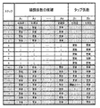
- FIG. 2 is a diagram for explaining an update process for reducing the convergence time.
- the update processing unit 204 first converges by an iterative method only for the compensation coefficient A i (a compensation coefficient selected according to the amplitude of the baseband signal x t among A 1 to A 8 ). The calculation is executed for a predetermined time, and the compensation coefficient A i is sequentially updated (steps 0 to 4 in FIG. 2). During this time, the values of tap coefficients B 1 and B 2 are set to constant values (initial values).
- the update processing unit 204 executes convergence calculation by the iterative method only for the tap coefficients B 1 and B 2 for a predetermined time, and sequentially updates the tap coefficients B 1 and B 2 (Steps 5 to 5 in FIG. 2). 9).
- the value of the compensation coefficient A i is set to a constant value (the value last updated in step 4 in FIG. 2).
- the update processing unit 204 the compensation coefficient A i, and applies the iterative method for both the tap coefficients B 1, B 2, compensation coefficients A i, and, both of the tap coefficients B 1, B 2 Update sequentially (steps 10 to 18 in FIG. 2).
- the update processing unit 204 considers that the coefficient is 0, and the absolute value of the convergence value becomes smaller than the predetermined threshold.
- the compensation coefficient or tap coefficient is excluded from the target of the convergence calculation.
- B k 0 is set.
- the absolute value of the converged value of the tap coefficient B 1 at step 14 is shown an example of when it becomes smaller than a predetermined threshold value.
- the distortion compensation device and the distortion compensation method according to the present invention are suitable for use in a distortion compensation device and a distortion compensation method for compensating for distortion of an output signal output from a predetermined circuit.
Landscapes
- Engineering & Computer Science (AREA)
- Power Engineering (AREA)
- Physics & Mathematics (AREA)
- Nonlinear Science (AREA)
- Computer Networks & Wireless Communication (AREA)
- Signal Processing (AREA)
- Amplifiers (AREA)
- Transmitters (AREA)
Abstract
L'invention concerne un dispositif de compensation de la distorsion qui peut à la fois effectuer une compensation de la distorsion avec une grande précision et réduire le volume d'espace de stockage occupé par des coefficients requis pour les calculs de compensation de la distorsion. Ledit dispositif de compensation de la distorsion (100) emploie la prédistortion, dans laquelle un signal d'entrée est prémultiplié par des coefficients, pour compenser la distortion dans un signal de sortie délivré par un circuit donné. Une première unité de multiplication (200c) dans ce dispositif de compensation de la distorsion (100) multiplie un signal d'entrée par des coefficients de compensation sélectionnés parmi des coefficients de compensation candidats en fonction du signal d'entrée. Des deuxièmes unités de multiplication (201c1 à 201cm) multiplient une version retardée du signal d'entrée par des coefficients de pondération et une unité d'addition (202) délivre, vers un circuit donné, un signal obtenu en additionnant ensemble le signal d'entrée multiplié par le coefficient de compensation et le signal d'entrée retardé multiplié par le coefficient de pondération.
Priority Applications (1)
| Application Number | Priority Date | Filing Date | Title |
|---|---|---|---|
| US14/655,217 US9531332B2 (en) | 2012-12-26 | 2013-11-29 | Distortion-compensation device and distortion-compensation method |
Applications Claiming Priority (2)
| Application Number | Priority Date | Filing Date | Title |
|---|---|---|---|
| JP2012-282752 | 2012-12-26 | ||
| JP2012282752A JP6054739B2 (ja) | 2012-12-26 | 2012-12-26 | 歪み補償装置及び歪み補償方法 |
Publications (1)
| Publication Number | Publication Date |
|---|---|
| WO2014103175A1 true WO2014103175A1 (fr) | 2014-07-03 |
Family
ID=51020303
Family Applications (1)
| Application Number | Title | Priority Date | Filing Date |
|---|---|---|---|
| PCT/JP2013/007043 Ceased WO2014103175A1 (fr) | 2012-12-26 | 2013-11-29 | Dispositif de compensation de la distorsion et procédé de compensation de la distorsion |
Country Status (3)
| Country | Link |
|---|---|
| US (1) | US9531332B2 (fr) |
| JP (1) | JP6054739B2 (fr) |
| WO (1) | WO2014103175A1 (fr) |
Families Citing this family (8)
| Publication number | Priority date | Publication date | Assignee | Title |
|---|---|---|---|---|
| US20180054170A1 (en) * | 2016-08-19 | 2018-02-22 | Fujitsu Limited | Distortion compensation device and coefficient update method |
| US9942074B1 (en) | 2016-11-30 | 2018-04-10 | Micron Technology, Inc. | Wireless devices and systems including examples of mixing coefficient data specific to a processing mode selection |
| US10027523B2 (en) | 2016-11-30 | 2018-07-17 | Micron Technology, Inc. | Wireless devices and systems including examples of mixing input data with coefficient data |
| US11005430B2 (en) | 2017-03-02 | 2021-05-11 | Sumitomo Electric Industries, Ltd. | Distortion compensation device and distortion compensation method |
| WO2019233555A1 (fr) * | 2018-06-05 | 2019-12-12 | Telefonaktiebolaget Lm Ericsson (Publ) | Mise en œuvre de faible puissance de prédistorsion numérique |
| US10886998B2 (en) | 2019-02-22 | 2021-01-05 | Micron Technology, Inc. | Mixing coefficient data specific to a processing mode selection using layers of multiplication/accumulation units for wireless communication |
| JP2021074080A (ja) * | 2019-11-06 | 2021-05-20 | ソニーセミコンダクタソリューションズ株式会社 | 信号処理回路 |
| US10924152B1 (en) | 2019-11-13 | 2021-02-16 | Micron Technology, Inc. | Mixing coefficient data for processing mode selection |
Citations (5)
| Publication number | Priority date | Publication date | Assignee | Title |
|---|---|---|---|---|
| WO2009090825A1 (fr) * | 2008-01-15 | 2009-07-23 | Mitsubishi Electric Corporation | Dispositif de précorrection |
| JP2010518660A (ja) * | 2006-12-26 | 2010-05-27 | ダリ システムズ カンパニー リミテッド | 多チャンネル広帯域通信システムにおけるベースバンドプリディストーション線形化の方法及びシステム |
| JP2010183525A (ja) * | 2009-02-09 | 2010-08-19 | Hitachi Kokusai Electric Inc | プリディストータ |
| JP2011135143A (ja) * | 2009-12-22 | 2011-07-07 | Hitachi Kokusai Electric Inc | プリディストーション方式の歪補償装置 |
| JP2011176686A (ja) * | 2010-02-25 | 2011-09-08 | Nec Corp | 前置歪み補償回路及び電力増幅器のメモリ効果歪み補償方法 |
Family Cites Families (3)
| Publication number | Priority date | Publication date | Assignee | Title |
|---|---|---|---|---|
| JP3560398B2 (ja) | 1995-08-31 | 2004-09-02 | 富士通株式会社 | 歪補償を有する増幅器 |
| JP4086133B2 (ja) | 1999-07-28 | 2008-05-14 | 富士通株式会社 | 無線装置の歪補償方法及び歪補償装置 |
| JP5301831B2 (ja) * | 2005-06-30 | 2013-09-25 | 富士通株式会社 | 歪補償回路を有する電力増幅器 |
-
2012
- 2012-12-26 JP JP2012282752A patent/JP6054739B2/ja not_active Expired - Fee Related
-
2013
- 2013-11-29 US US14/655,217 patent/US9531332B2/en not_active Expired - Fee Related
- 2013-11-29 WO PCT/JP2013/007043 patent/WO2014103175A1/fr not_active Ceased
Patent Citations (5)
| Publication number | Priority date | Publication date | Assignee | Title |
|---|---|---|---|---|
| JP2010518660A (ja) * | 2006-12-26 | 2010-05-27 | ダリ システムズ カンパニー リミテッド | 多チャンネル広帯域通信システムにおけるベースバンドプリディストーション線形化の方法及びシステム |
| WO2009090825A1 (fr) * | 2008-01-15 | 2009-07-23 | Mitsubishi Electric Corporation | Dispositif de précorrection |
| JP2010183525A (ja) * | 2009-02-09 | 2010-08-19 | Hitachi Kokusai Electric Inc | プリディストータ |
| JP2011135143A (ja) * | 2009-12-22 | 2011-07-07 | Hitachi Kokusai Electric Inc | プリディストーション方式の歪補償装置 |
| JP2011176686A (ja) * | 2010-02-25 | 2011-09-08 | Nec Corp | 前置歪み補償回路及び電力増幅器のメモリ効果歪み補償方法 |
Also Published As
| Publication number | Publication date |
|---|---|
| US20150349725A1 (en) | 2015-12-03 |
| JP6054739B2 (ja) | 2016-12-27 |
| JP2014127829A (ja) | 2014-07-07 |
| US9531332B2 (en) | 2016-12-27 |
Similar Documents
| Publication | Publication Date | Title |
|---|---|---|
| JP6054739B2 (ja) | 歪み補償装置及び歪み補償方法 | |
| US9397619B2 (en) | Distortion compensation apparatus and distortion compensation method | |
| US8737937B2 (en) | Distortion compensation apparatus, transmitter, and distortion compensation method | |
| EP1560329A1 (fr) | Dispositif de prédistorsion digital utilisant un modèle à base de séries de puissances | |
| US8933752B2 (en) | Power amplifier apparatus, distortion compensation coefficient updating method, and transmission apparatus | |
| US10797737B2 (en) | Distortion compensation device and distortion compensation method | |
| JP5124655B2 (ja) | 歪補償増幅器 | |
| US9450544B2 (en) | Pre-distortion method, associated apparatus and non-transitory machine readable medium | |
| JP5707999B2 (ja) | 歪補償装置、送信機及び歪補償方法 | |
| WO2006095422A1 (fr) | Dispositif de compensation de deformation | |
| US20090227216A1 (en) | Apparatus for updating coefficient for distortion compensation and amplifier for compensating distortion | |
| US9853664B2 (en) | Radio frequency power amplification system, radio frequency power amplification method, transmitter, and base station | |
| JP2006279780A (ja) | 歪み補償装置及び歪み補償方法 | |
| US9438177B2 (en) | Pre-distortion method and associated apparatus and non-transitory machine readable medium | |
| US20180013456A1 (en) | Distortion compensation device and distortion compensation method | |
| US9548703B2 (en) | Distortion compensation apparatus, transmission apparatus, and distortion compensation method | |
| JP5387445B2 (ja) | 前置歪み補償回路及び電力増幅器のメモリ効果歪み補償方法 | |
| JP6015386B2 (ja) | 歪補償装置及び歪補償方法 | |
| US9768891B2 (en) | Distortion compensation device and distortion compensation method | |
| JP2015023507A (ja) | 歪み補償装置 | |
| US9680511B1 (en) | Distortion compensator, distortion compensation method and radio equipment | |
| JP2008236592A (ja) | 受信装置および無線装置 | |
| JP2005079935A (ja) | 適応プリディストーション型歪補償電力増幅器 | |
| KR100939882B1 (ko) | 왜곡 보상 장치 | |
| JP2006295440A (ja) | 歪補償装置および遅延量制御方法 |
Legal Events
| Date | Code | Title | Description |
|---|---|---|---|
| 121 | Ep: the epo has been informed by wipo that ep was designated in this application |
Ref document number: 13868573 Country of ref document: EP Kind code of ref document: A1 |
|
| WWE | Wipo information: entry into national phase |
Ref document number: 14655217 Country of ref document: US |
|
| NENP | Non-entry into the national phase |
Ref country code: DE |
|
| 122 | Ep: pct application non-entry in european phase |
Ref document number: 13868573 Country of ref document: EP Kind code of ref document: A1 |