WO2014103235A1 - Dispositif de calcul et procédé de calcul - Google Patents
Dispositif de calcul et procédé de calcul Download PDFInfo
- Publication number
- WO2014103235A1 WO2014103235A1 PCT/JP2013/007383 JP2013007383W WO2014103235A1 WO 2014103235 A1 WO2014103235 A1 WO 2014103235A1 JP 2013007383 W JP2013007383 W JP 2013007383W WO 2014103235 A1 WO2014103235 A1 WO 2014103235A1
- Authority
- WO
- WIPO (PCT)
- Prior art keywords
- data
- unit
- arithmetic
- rearrangement
- arithmetic processing
- Prior art date
- Legal status (The legal status is an assumption and is not a legal conclusion. Google has not performed a legal analysis and makes no representation as to the accuracy of the status listed.)
- Ceased
Links
Images



Classifications
-
- G—PHYSICS
- G06—COMPUTING OR CALCULATING; COUNTING
- G06F—ELECTRIC DIGITAL DATA PROCESSING
- G06F15/00—Digital computers in general; Data processing equipment in general
- G06F15/76—Architectures of general purpose stored program computers
- G06F15/80—Architectures of general purpose stored program computers comprising an array of processing units with common control, e.g. single instruction multiple data processors
-
- G—PHYSICS
- G06—COMPUTING OR CALCULATING; COUNTING
- G06F—ELECTRIC DIGITAL DATA PROCESSING
- G06F3/00—Input arrangements for transferring data to be processed into a form capable of being handled by the computer; Output arrangements for transferring data from processing unit to output unit, e.g. interface arrangements
- G06F3/06—Digital input from, or digital output to, record carriers, e.g. RAID, emulated record carriers or networked record carriers
- G06F3/0601—Interfaces specially adapted for storage systems
- G06F3/0628—Interfaces specially adapted for storage systems making use of a particular technique
- G06F3/0646—Horizontal data movement in storage systems, i.e. moving data in between storage devices or systems
- G06F3/0647—Migration mechanisms
-
- G—PHYSICS
- G06—COMPUTING OR CALCULATING; COUNTING
- G06F—ELECTRIC DIGITAL DATA PROCESSING
- G06F12/00—Accessing, addressing or allocating within memory systems or architectures
-
- G—PHYSICS
- G06—COMPUTING OR CALCULATING; COUNTING
- G06F—ELECTRIC DIGITAL DATA PROCESSING
- G06F12/00—Accessing, addressing or allocating within memory systems or architectures
- G06F12/02—Addressing or allocation; Relocation
- G06F12/06—Addressing a physical block of locations, e.g. base addressing, module addressing, memory dedication
-
- G—PHYSICS
- G06—COMPUTING OR CALCULATING; COUNTING
- G06F—ELECTRIC DIGITAL DATA PROCESSING
- G06F15/00—Digital computers in general; Data processing equipment in general
- G06F15/16—Combinations of two or more digital computers each having at least an arithmetic unit, a program unit and a register, e.g. for a simultaneous processing of several programs
- G06F15/163—Interprocessor communication
- G06F15/167—Interprocessor communication using a common memory, e.g. mailbox
-
- G—PHYSICS
- G06—COMPUTING OR CALCULATING; COUNTING
- G06F—ELECTRIC DIGITAL DATA PROCESSING
- G06F3/00—Input arrangements for transferring data to be processed into a form capable of being handled by the computer; Output arrangements for transferring data from processing unit to output unit, e.g. interface arrangements
- G06F3/06—Digital input from, or digital output to, record carriers, e.g. RAID, emulated record carriers or networked record carriers
- G06F3/0601—Interfaces specially adapted for storage systems
- G06F3/0602—Interfaces specially adapted for storage systems specifically adapted to achieve a particular effect
- G06F3/0608—Saving storage space on storage systems
-
- G—PHYSICS
- G06—COMPUTING OR CALCULATING; COUNTING
- G06F—ELECTRIC DIGITAL DATA PROCESSING
- G06F3/00—Input arrangements for transferring data to be processed into a form capable of being handled by the computer; Output arrangements for transferring data from processing unit to output unit, e.g. interface arrangements
- G06F3/06—Digital input from, or digital output to, record carriers, e.g. RAID, emulated record carriers or networked record carriers
- G06F3/0601—Interfaces specially adapted for storage systems
- G06F3/0668—Interfaces specially adapted for storage systems adopting a particular infrastructure
- G06F3/0671—In-line storage system
- G06F3/0683—Plurality of storage devices
-
- G—PHYSICS
- G06—COMPUTING OR CALCULATING; COUNTING
- G06F—ELECTRIC DIGITAL DATA PROCESSING
- G06F7/00—Methods or arrangements for processing data by operating upon the order or content of the data handled
- G06F7/76—Arrangements for rearranging, permuting or selecting data according to predetermined rules, independently of the content of the data
-
- G—PHYSICS
- G06—COMPUTING OR CALCULATING; COUNTING
- G06F—ELECTRIC DIGITAL DATA PROCESSING
- G06F9/00—Arrangements for program control, e.g. control units
- G06F9/06—Arrangements for program control, e.g. control units using stored programs, i.e. using an internal store of processing equipment to receive or retain programs
- G06F9/30—Arrangements for executing machine instructions, e.g. instruction decode
- G06F9/30003—Arrangements for executing specific machine instructions
- G06F9/30007—Arrangements for executing specific machine instructions to perform operations on data operands
- G06F9/30032—Movement instructions, e.g. MOVE, SHIFT, ROTATE, SHUFFLE
-
- G—PHYSICS
- G06—COMPUTING OR CALCULATING; COUNTING
- G06F—ELECTRIC DIGITAL DATA PROCESSING
- G06F9/00—Arrangements for program control, e.g. control units
- G06F9/06—Arrangements for program control, e.g. control units using stored programs, i.e. using an internal store of processing equipment to receive or retain programs
- G06F9/30—Arrangements for executing machine instructions, e.g. instruction decode
- G06F9/34—Addressing or accessing the instruction operand or the result ; Formation of operand address; Addressing modes
-
- G—PHYSICS
- G06—COMPUTING OR CALCULATING; COUNTING
- G06F—ELECTRIC DIGITAL DATA PROCESSING
- G06F3/00—Input arrangements for transferring data to be processed into a form capable of being handled by the computer; Output arrangements for transferring data from processing unit to output unit, e.g. interface arrangements
- G06F3/06—Digital input from, or digital output to, record carriers, e.g. RAID, emulated record carriers or networked record carriers
- G06F3/0601—Interfaces specially adapted for storage systems
- G06F3/0602—Interfaces specially adapted for storage systems specifically adapted to achieve a particular effect
- G06F3/0604—Improving or facilitating administration, e.g. storage management
- G06F3/0607—Improving or facilitating administration, e.g. storage management by facilitating the process of upgrading existing storage systems, e.g. for improving compatibility between host and storage device
-
- G—PHYSICS
- G06—COMPUTING OR CALCULATING; COUNTING
- G06F—ELECTRIC DIGITAL DATA PROCESSING
- G06F3/00—Input arrangements for transferring data to be processed into a form capable of being handled by the computer; Output arrangements for transferring data from processing unit to output unit, e.g. interface arrangements
- G06F3/06—Digital input from, or digital output to, record carriers, e.g. RAID, emulated record carriers or networked record carriers
- G06F3/0601—Interfaces specially adapted for storage systems
- G06F3/0668—Interfaces specially adapted for storage systems adopting a particular infrastructure
- G06F3/067—Distributed or networked storage systems, e.g. storage area networks [SAN], network attached storage [NAS]
-
- G—PHYSICS
- G06—COMPUTING OR CALCULATING; COUNTING
- G06F—ELECTRIC DIGITAL DATA PROCESSING
- G06F3/00—Input arrangements for transferring data to be processed into a form capable of being handled by the computer; Output arrangements for transferring data from processing unit to output unit, e.g. interface arrangements
- G06F3/06—Digital input from, or digital output to, record carriers, e.g. RAID, emulated record carriers or networked record carriers
- G06F3/0601—Interfaces specially adapted for storage systems
- G06F3/0668—Interfaces specially adapted for storage systems adopting a particular infrastructure
- G06F3/0671—In-line storage system
- G06F3/0683—Plurality of storage devices
- G06F3/0689—Disk arrays, e.g. RAID, JBOD
Definitions
- the present invention relates to an arithmetic device including a plurality of arithmetic processing units (processors), and more particularly to an arithmetic device that rearranges data.
- processors arithmetic processing units
- Signal processing treats a large amount of continuous data (stream data) as calculation target data.
- stream data continuous data
- the same processing operation that can be realized using a plurality of instructions
- An array processor is one of processor architectures for efficiently processing a large amount of data.
- FIG. 7 is a block diagram showing an example of the configuration of a general array processor 19.
- the array processor 19 shown in FIG. 7 includes a plurality of arithmetic processing units 11a to 11d (hereinafter collectively referred to as the arithmetic processing unit 11) and arithmetic processing units 12a to 12d (hereinafter collectively referred to as the arithmetic processing unit 12).
- Array operation unit 14 arranged in an array.
- each arithmetic processing unit included in the array arithmetic unit 14, that is, the arithmetic processing unit 11 and the arithmetic processing unit 12 are collectively referred to as an arithmetic processing unit 15.
- the array processor 19 includes memory banks 10a to 10d (hereinafter collectively referred to as the memory bank 10) and memory banks 13a to 13d (hereinafter collectively referred to as the memory bank 13) connected to the array calculation unit 14.
- a data memory 17 is included.
- memory bank 10 and memory bank 13 are collectively referred to as multi-bank 16).
- the arithmetic processing units 15 arranged in an array are connected to neighboring arithmetic processing units 15.
- Wirings are connected between the arithmetic processing units 15 like meshes. Each connection is controlled by a switch in the input stage of the arithmetic processing unit 15. Data to be calculated is stored in the memory bank 10 and the memory bank 13 of the multi-bank 16 connected to the array calculation unit 14.
- the array calculation unit 14 has different degrees of parallelism and flexibility in calculation processing based on the internal connection configuration.
- the arithmetic processing unit 15 is connected to a neighboring arithmetic processing unit 15 as shown in FIG.
- the array processor 19 executes a predetermined process in cooperation with the plurality of arithmetic processing units 15. For this reason, if the timing of the data that arrives at the arithmetic processing unit 15 and the input data is different, the array processor 19 may not be able to appropriately perform the arithmetic operation.
- the calculation of the arithmetic processing part 12b requires the calculation result of the arithmetic processing part 11b and the arithmetic processing part 12a.
- the calculation execution timings of the calculation processing unit 11b and the calculation processing unit 12a are different, the input timing of each calculation result from the calculation processing unit 11b and the calculation processing unit 12a to the calculation processing unit 12b is determined based on the timing. , There will be a difference.
- the input of the respective operation results from the arithmetic processing unit 11b and the arithmetic processing unit 12a to the arithmetic processing unit 12b based on the delay difference.
- FIG. 8 is a block diagram showing an example of the configuration of the array processor 29 using a FIFO (First In In First Out) memory as a synchronization mechanism.
- FIFO First In In First Out
- the array processor 29 includes arithmetic processing units 21a to 21d (hereinafter collectively referred to as arithmetic processing unit 21) and arithmetic processing units 22a to 22d (hereinafter collectively referred to as arithmetic processing unit 22). Including.
- the array processor 29 includes memory banks 20a to 20d (hereinafter collectively referred to as memory bank 20) and memory banks 23a to 23d (hereinafter collectively referred to as memory bank 23).
- the array processor 29 connects the input / output of the arithmetic processing unit 21, the arithmetic processing unit 22, the memory bank 20, and the memory bank 23 via the FIFOs 24a to 24g, the FIFOs 25a to 25g, and the FIFOs 26a to 26d.
- the FIFOs 24a to 24g are collectively referred to as the FIFO 24.
- the FIFOs 25a to 25g are collectively referred to as a FIFO 25.
- the FIFOs 26a to 26d are collectively referred to as a FIFO 26.
- the array processor 29 then synchronizes input / output data with synchronization control units 27a to 27d (hereinafter collectively referred to as synchronization control unit 27) and synchronization control units 28a to 28d (hereinafter collectively referred to as synchronization control unit 28). including.
- the synchronization control unit 27 and the synchronization control unit 28 use the FIFO 24, the FIFO 25, and the FIFO 26 to control data that reaches the memory bank 20, the memory bank 23, the arithmetic processing unit 21, and the arithmetic processing unit 22.
- the arithmetic processing unit 21 and the arithmetic processing unit 22 use the synchronization control unit 27 and the synchronization control unit 28 to enable synchronization control when the input data to be reached is different for each input port.
- An object of the present invention is to provide an arithmetic device and an arithmetic processing method that solve the above-described problems of reduction in arithmetic efficiency, increase in circuit scale, and increase in power consumption.
- An arithmetic device includes a first data storage unit that stores data to be calculated, an arithmetic processing unit that executes an operation using data, and the arithmetic unit stored in the first data storage unit. Select the designated data from the target data and the data computed by the computation processing means, and based on the parameters, give a predetermined delay to the data that received a delay instruction among the designated data, The data not subjected to the delay instruction is not delayed, the instructed data is rearranged based on the parameters, and the data calculated in the arithmetic processing means and the operation result data of the arithmetic processing means are output. And a second data storage means for storing the operation result data output from the data rearrangement means.
- the calculation method stores calculation target data, calculates using the data, selects the specified data from the stored calculation target data and the calculated data, and based on the parameters A predetermined delay is given to the data that has been instructed to delay among the instructed data, and the data that has not been instructed to be delayed is not delayed, and the instructed data is rearranged based on the parameters. Then, the calculated data and calculation result data are output, and the calculation result data is stored.
- a recording medium on which a computer-readable program according to an embodiment of the present invention is recorded includes a process for storing calculation target data, a process for calculating using the data, the stored calculation target data, and the calculated data. Select the specified data from among the parameters, and based on the parameters, give a predetermined delay to the data that has received a delay instruction, and do not delay the data that has not received a delay instruction. Based on the above, a program for executing the rearrangement of the instructed data, outputting the calculated data and the calculation result data, and storing the calculation result data is recorded.
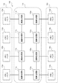
- FIG. 1 is a block diagram showing an example of the configuration of the arithmetic device according to the first embodiment of the present invention.
- FIG. 2 is a block diagram illustrating an example of the configuration of the data rearrangement unit according to the first embodiment.
- FIG. 3 is a block diagram illustrating an example of another configuration of the arithmetic device according to the first embodiment.
- FIG. 4 is a block diagram illustrating an example of another configuration of the arithmetic device according to the first embodiment.
- FIG. 5 is a block diagram illustrating an example of another configuration of the arithmetic device according to the first embodiment.
- FIG. 6 is a block diagram illustrating an example of the configuration of the data rearrangement unit according to the first embodiment.
- FIG. 7 is a block diagram showing a configuration of a general array processor.
- FIG. 8 is a block diagram showing a configuration of an array processor equipped with a general synchronization mechanism.
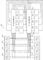
- FIG. 1 is a block diagram showing an example of the configuration of the arithmetic unit 37 according to the first embodiment of the present invention.
- the arithmetic unit 37 includes memory banks 30a to 30d, memory banks 33a to 33d, arithmetic processing units 31a to 31d, arithmetic processing units 32a to 32d, and data rearranging units 34a to 34b.
- the memory banks 30a to 30d are collectively referred to as a memory bank 30.
- the memory banks 33a to 33d are collectively referred to as a memory bank 33.
- the arithmetic processing units 31a to 31d are collectively referred to as an arithmetic processing unit 31.
- the arithmetic processing units 32a to 32d are collectively referred to as an arithmetic processing unit 32.
- the data rearranging units 34a to 34b are collectively referred to as a data rearranging unit 34.
- the arithmetic device 37 of the present embodiment connects the data rearrangement unit 34 a, the arithmetic processing unit 31, the data rearrangement unit 34 b, and the arithmetic processing unit 32 in a ring shape. To do.
- the memory bank 30 is connected to the data rearrangement unit 34a and the data rearrangement unit 34b.
- the memory bank 33 is connected to the data rearrangement unit 34a and the data rearrangement unit 34b.
- the memory bank 30 and the memory bank 33 store calculation data. Therefore, it can be said that the memory bank 30 and the memory bank 33 are data storage units.
- Calculation data is data including data to be calculated (calculation target data) and data to be a calculation result (calculation result data).
- the purpose of use of the memory bank 30 and the memory bank 33 is not limited. Any one of the memory banks 30 and 33 may hold the calculation target data, and the remaining memory banks may store the calculation result data.
- the memory bank 30 may hold calculation target data, and the memory bank 33 may hold calculation result data.
- the memory bank 33 may hold calculation target data, and the memory bank 30 may store calculation result data.
- a part of the memory bank 30 and the memory bank 33 may hold the operation target data, and the remaining memory bank 30 and the memory bank 33 may store the operation result data.
- the memory bank 30 and the memory bank 33 may hold other data.
- the memory bank 30 or the memory bank 33 may hold parameters described later.
- the memory bank 30 holds operation target data and the memory bank 33 stores operation result data.
- the data rearrangement unit 34 a is connected to the operation processing unit 32 at the preceding stage, the operation processing unit 31 at the subsequent stage, the memory bank 30, and the memory bank 33.
- the data rearrangement unit 34 b is connected to the operation processing unit 31 that is the preceding stage, the operation processing unit 32 that is the subsequent stage, the memory bank 30, and the memory bank 33.
- the data rearrangement unit 34a supplies the data of the processing result of the preceding arithmetic processing unit 32 or the data of the memory bank 30 to the subsequent arithmetic processing unit 31 connected as an output destination at an appropriate timing. Therefore, the data rearrangement unit 34a rearranges the data in the time direction, selects the arithmetic processing unit 31 that supplies the data, and supplies the data.
- the data rearrangement unit 34b supplies the processing result data of the preceding arithmetic processing unit 31 or the data of the memory bank 30 to the subsequent arithmetic processing unit 32 connected as an output destination at an appropriate timing.
- the data rearrangement unit 34b rearranges the data in the time direction, selects the arithmetic processing unit 32 that supplies the data, and supplies the data.
- the plurality of calculation processing units 31 and the calculation processing unit 32 execute element calculations necessary for predetermined calculation processing.
- the arithmetic processing unit 31 and the arithmetic processing unit 32 execute four arithmetic operations, logical operations, accumulation, or power calculation.
- the arithmetic operations performed by the arithmetic processing unit 31 and the arithmetic processing unit 32 of the present embodiment are not particularly limited.
- the arithmetic processing unit 31 is connected to the data rearrangement unit 34a at the previous stage and the data rearrangement unit 34b at the rear stage.
- the arithmetic processing unit 31 receives the data of the memory bank 30 from the data rearrangement unit 34a, processes a predetermined calculation, and outputs the calculation result to the data rearrangement unit 34b.
- the arithmetic processing unit 32 is connected to the data rearrangement unit 34b in the previous stage and the data rearrangement unit 34a in the rear stage.
- the arithmetic processing unit 32 receives the data of the memory bank 30 and the calculation result of the calculation processing unit 32 from the data rearrangement unit 34b, processes a predetermined calculation, and outputs the calculation result to the data rearrangement unit 34a.
- the arithmetic processing unit 31 is referred to as a “first arithmetic processing unit” and the arithmetic processing unit 32 is referred to as a “second arithmetic processing unit” as necessary.
- the data rearrangement unit 34a is referred to as a “first data rearrangement unit”, and the data rearrangement unit 34b is referred to as a “second data rearrangement unit”.
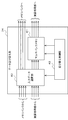
- FIG. 2 is a block diagram showing an example of the configuration of the data rearrangement unit 34. As shown in FIG.
- the data rearrangement unit 34 includes an input data selection unit 40, a multi-bank memory 41, and a rearrangement control unit 42.
- the input data selection unit 40 is connected to the memory bank 30, the memory bank 33, the previous arithmetic processing unit (the arithmetic processing unit 31 or the arithmetic processing unit 32), the multi-bank memory 41, and the rearrangement control unit 42. .
- the input data selection unit 40 selects an arithmetic processing unit that outputs the input data from the memory bank 30 and the input data from the previous arithmetic processing unit.
- the input data selection unit 40 of the data rearrangement unit 34a selects the arithmetic processing unit 31 that outputs the input data from the memory bank 30 and the input data of the previous arithmetic processing unit 32.
- the input data selection unit 40 of the data rearrangement unit 34b selects the arithmetic processing unit 32 that outputs the input data from the memory bank 30 and the input data of the previous arithmetic processing unit 31.
- the input data selection unit 40 selects whether or not to output the input data from the previous arithmetic processing unit to the memory bank 33.
- the input data selection unit 40 of the data rearrangement unit 34 a selects whether or not to output the input data from the previous arithmetic processing unit 32 to the memory bank 33.
- the input data selection unit 40 of the data rearrangement unit 34b selects whether or not to output the input data from the previous arithmetic processing unit 31 to the memory bank 33.
- the multi-bank memory 41 is a multi-port memory having a plurality of ports.
- the multi-bank memory 41 shown in FIG. 2 has four ports as the number of boats, but this is merely an example.
- the multi-bank memory 41 of the present embodiment may have a port number less than 4, or may have a port number greater than 4.
- the multi-bank memory 41 is connected to the input data selection unit 40, the arithmetic processing unit 31 or the arithmetic processing unit 32, and the rearrangement control unit 42.
- the multi-bank memory 41 receives a write or read timing signal or instruction from the rearrangement control unit 42. Further, the multi-bank memory 41 receives an instruction for a write port and a read port from the rearrangement control unit 42. Based on these, the multi-bank memory 41 stores the received data, rearranges the data in the output port direction, and rearranges the data in the time direction.
- the above operation will be described using the 4-port multi-bank memory 41 shown in FIG.
- the port numbers are 0, 1, 2, and 3, respectively.
- the port numbers (0th port to 3rd port) correspond to the symbols (ad) of the respective components.
- the multi-bank memory 41 sends out the data written from the 0th port to the 2nd port based on the instruction. As a result, for example, the multi-bank memory 41 transfers the data from the arithmetic processing unit 31a to the arithmetic processing unit 32c.
- the multi-bank memory 41 sends out the data written in the Nth cycle based on the instruction in the (N + 4) th cycle.
- the multi-bank memory 41 delays data by 4 cycles in the time direction.
- the multi-bank memory 41 of the present embodiment is not particularly limited as long as it can simultaneously access a plurality of banks.
- the multi-bank memory 41 may be a general multi-port memory having a predetermined number of ports and a memory.
- the multi-bank memory 41 may be a memory device equipped with a crossbar for connecting a plurality of memories. Therefore, the multi-bank memory 41 can also be referred to as a “multi-port storage unit”.
- the rearrangement control unit 42 is connected to the input data selection unit 40 and the multi-bank memory 41.
- the rearrangement control unit 42 controls at least the selection operation of the input data selection unit 40 and the memory access of the multi-bank memory 41.
- the rearrangement control unit 42 has no particular restriction on the control method.
- the rearrangement control unit 42 may send an input data selection signal indicating selection of input data to the input data selection unit 40.
- the rearrangement control unit 42 may send a selection command to the input data selection unit 40.
- the rearrangement control unit 42 may send a write address and a read address to the multi-bank memory 41. Alternatively, the rearrangement control unit 42 may send a write command and a read command.
- the calculation targets data read from the memory bank 30 in parallel toward the calculation processing unit 31. Then, it is assumed that the results calculated by the arithmetic processing unit 31 and the arithmetic processing unit 32 are stored in the memory bank 33.
- Step 2 Using the data stored in the memory bank 30, the arithmetic processing unit 31 and the arithmetic processing unit 32 process a predetermined operation, and then write the operation result in the memory bank 33 (hereinafter referred to as “main operation”). Step).
- the parameters are transferred from the memory bank 30 to the data rearrangement unit 34 in parallel.
- the parameter is data instructing switching of data output ports and rearrangement of data in the time direction in the multi-bank memory 41, that is, rearrangement and delay of data.
- the parameters may be stored in the memory bank 30 before the arithmetic processing.
- a user who performs a calculation using the calculation device 37 stores the parameters in the memory bank 30 before the calculation process.
- the data rearrangement unit 34 is connected to the memory bank 30 so that parameters read from the memory bank 30 can be broadcast and input. Therefore, the data rearrangement unit 34a and the data rearrangement unit 34b according to the present embodiment can read from the memory bank 30 at a time even if the data is necessary for both.
- the transferred parameters are input to the input data selection unit 40 inside the data rearrangement unit 34. Then, the input data selection unit 40 selects necessary parameters based on the input data selection signal generated by the rearrangement control unit 42. Necessary parameters are stored in a predetermined location of the multi-bank memory 41 in accordance with the write address generated by the rearrangement control unit 42.
- the multi-bank memory 41 executes predetermined delay and rearrangement of data based on the parameters.
- the arithmetic unit 37 processes the main step (2) for the actual arithmetic processing.
- the operation data is transferred from the memory bank 30 to the data rearrangement unit 34a in parallel.
- the input data selection unit 40 of the data rearrangement unit 34a selects the input calculation data. Then, the input data selection unit 40 stores the operation data in the multi-bank memory 41 using the write address generated by the rearrangement control unit 42 of the data rearrangement unit 34a. At this time, the rearrangement control unit 42 counts the number of generated write addresses and determines the timing of read address generation.
- the rearrangement control unit 42 when the data transfer delay is 4 cycles, the rearrangement control unit 42 generates the first read address when the write address count number is 4 or more. Based on such an operation, the rearrangement control unit 42 realizes a predetermined data transfer delay.
- the rearrangement control unit 42 controls the read address generation timing and the address. Based on the operation of the rearrangement control unit 42, the arithmetic data is given a predetermined delay as described above, rearranged in the parallel direction, and transferred to the arithmetic processing unit 31 at a predetermined timing.
- the operation processing unit 31 When the operation data is input to the plurality of operation processing units 31, the operation processing unit 31 performs a predetermined operation.
- the data of the calculation result of the calculation processing unit 31 is transferred to the subsequent data rearrangement unit 34b.
- the data rearrangement unit 34b like the data rearrangement unit 34a, gives a predetermined delay to the input data (calculation result) in a predetermined parallel direction. Rearrangement and transfer to the arithmetic processing unit 32.
- the arithmetic processing unit 32 executes a predetermined calculation and transmits the data to the subsequent data rearranging unit 34a.
- the rearrangement control unit 42 of the data rearrangement unit 34a determines whether or not the input data is a target to be written back to the memory bank 33. To do. Then, the rearrangement control unit 42 supplies an input data selection signal according to the determination to the input data selection unit 40 of the data rearrangement unit 34a. As a result, the input data is transferred to the memory bank 33.
- the computing device 37 can repeat the above processing as many times as the number of data to realize a predetermined computation.
- each part of the arithmetic unit 37 may execute processing in a pipeline manner.
- the data rearrangement unit 34 does not use a complicated rearrangement process for clarification of the explanation.
- the arithmetic unit 37 can realize arithmetic processing having complicated data transfer (or connection of arithmetic processing units) based on the same operation as described above. For example, if the data rearrangement unit 34 of the arithmetic device 37 appropriately executes the data rearrangement, the arithmetic processing unit 31 and the arithmetic processing unit 32 can execute a predetermined arithmetic operation efficiently while performing a cooperative operation.
- the arithmetic processing unit 31 and the arithmetic processing unit 32 have performed the arithmetic processing once.
- the arithmetic device 37 does not have to limit the number of processes of the arithmetic processing unit 31 and the arithmetic processing unit 32 to one.
- the data rearrangement unit 34, the arithmetic processing unit 31, and the arithmetic processing unit 32 are connected in a ring shape as shown in FIG.
- the arithmetic unit 37 can process arithmetic operations on a scale exceeding the number of stages in the arithmetic processing unit based on the following operations.
- the data rearrangement unit 34 a rearranges the data in the memory bank 30 as necessary, selects the data, and transfers it to the arithmetic processing unit 31.
- the calculation processing unit 31 processes a predetermined calculation and transfers it to the data rearrangement unit 34b.
- the data rearrangement unit 34b rearranges the data in the memory bank 30 and the operation result of the operation processing unit 31 as necessary, selects the data, and transfers it to the operation processing unit 32.
- the calculation processing unit 32 processes a predetermined calculation and transfers it to the data rearrangement unit 34a.
- the data rearrangement unit 34 a selects the processing result of the arithmetic processing unit 32 and sends it to the memory bank 33.
- the data rearrangement unit 34a rearranges the data in the memory bank 30 and the processing result of the arithmetic processing unit 32 as necessary, and then selects and transfers the data to the arithmetic processing unit 31.
- the data rearrangement unit 34 a selects and transfers the calculation result to the memory bank 33 when the final calculation result is included in the received calculation result. Specifically, the input data selection unit 40 transfers the processing result of the arithmetic processing unit 32 to the memory bank 33 based on an instruction from the rearrangement control unit 43.
- the calculation processing unit 31 processes a predetermined calculation and transfers it to the data rearrangement unit 34b.
- the data rearrangement unit 34b rearranges the data in the memory bank 30 and the operation result of the operation processing unit 31 as necessary, and then selects and transfers the data to the operation processing unit 32. Further, when the received calculation result includes a final calculation result, the data rearrangement unit 34 b transfers the calculation result to the memory bank 33.
- the calculation device 37 repeats this process until the predetermined calculation process is completed.
- the data rearrangement unit 34b transfers the final operation result to the memory bank 33 when receiving the first operation result. Also good. In this case, as described above, the input data selection unit 40 of the data rearrangement unit 34 b transfers the calculation result to the memory bank 33.
- the arithmetic device 37 of the present embodiment can realize processing exceeding the number of stages in the arithmetic processing unit.
- the data that can be selected by the input data selection unit 40 of the data rearrangement unit 34 is data from the memory bank 30 and data from the previous arithmetic processing unit.
- the computing device 37 of the present embodiment is not limited to this.
- the data rearrangement unit 34 may receive and select data from the subsequent arithmetic processing unit in addition to the previous stage.
- FIG. 3 is a block diagram illustrating an example of the configuration of the arithmetic device 38 including another configuration of the present embodiment.
- the data rearrangement unit 34 of the arithmetic device 38 is connected to the memory bank 30, the memory bank 33, the arithmetic processing unit 31, and the arithmetic processing unit 32. Then, the data rearrangement unit 34 of the arithmetic device 38 receives and selects data from the memory bank 30, the arithmetic processing unit 31, and the arithmetic processing unit 32.
- the arithmetic unit 38 configured as described above can input the calculation result of the subsequent arithmetic processing unit in addition to the memory bank 30 and the previous arithmetic processing unit to the arithmetic processing unit. Therefore, the calculation device 38 can execute more sophisticated or efficient calculations.
- calculation device 37 including the calculation device 38 will be described.
- the data rearrangement unit 34 includes a data rearrangement unit 34d and a data rearrangement unit 34e.
- the number of the memory bank 30, the memory bank 33, the arithmetic processing unit 31, and the arithmetic processing unit 32 included in the arithmetic device 37 of the present embodiment is four as an example.
- the computing device 37 of this embodiment may include each configuration of less than 4 or more than 4.
- the arithmetic unit 37 does not have to limit the number of data rearranging units 34 to two.
- the arithmetic device 37 may include more than two data rearranging units 34.
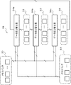
- FIG. 4 is a block diagram showing an example of the configuration of the arithmetic device 39 including three data rearranging units 34.
- the diagram becomes complicated, and therefore, an oblique line indicating that there are a plurality of connection lines is used.
- the arithmetic device 39 includes a data rearrangement unit 34a, a data rearrangement unit 34b, a data rearrangement unit 34c, a memory bank 30, a memory bank 33, an arithmetic processing unit 31, an arithmetic processing unit 32, and an arithmetic processing. Part 35.
- the data rearrangement unit 34c includes the same configuration as the data rearrangement unit 34b and operates in the same manner. Therefore, it can be said that the data rearrangement unit 34c of this embodiment is a part of the second data rearrangement unit.
- the arithmetic processing unit 35 includes the same configuration as the arithmetic processing unit 32 and operates in the same manner. Therefore, it can be said that the arithmetic processing unit 35 of the present embodiment is a part of the second arithmetic processing unit.
- the calculation processing unit 31, the calculation processing unit 32, and the calculation processing unit 35 can execute calculation processing in parallel.
- the arithmetic device 39 including such a configuration can execute more arithmetic processes in parallel than the arithmetic device 37.
- the calculation device 37 including the calculation device 39 will be described.
- the data rearrangement unit 34 includes a data rearrangement unit 34c.
- the arithmetic unit 37 may include one data rearrangement unit 34.
- FIG. 5 is a block diagram showing an example of the configuration of the arithmetic device 36 including one data rearrangement unit 34.
- the computing device 36 includes a data rearrangement unit 34a, a memory bank 30, a memory bank 33, and an arithmetic processing unit 31.
- the data rearrangement unit 34a of the calculation device 36 repeats the calculation of the calculation processing unit 31 as many times as necessary for the calculation.
- the arithmetic device 36 is an example of the minimum configuration of the present embodiment.
- calculation device 37 including the calculation device 36 will be described.
- the number of arithmetic processing units before and after the data rearrangement unit 34 in the arithmetic unit 37 may be different.
- the arithmetic unit 37 need not limit the number of the memory banks 30 and the memory banks 33 to four.
- the computing device 37 may include less than four memory banks 30 or memory banks 33 or may include more than four. Further, the arithmetic unit 37 may include a different number of memory banks 30 and memory banks 33.
- the arithmetic device 37 of the present embodiment can obtain the effect of increasing the arithmetic efficiency while suppressing the increase in circuit scale and power consumption.
- the data rearrangement unit 34 of the arithmetic device 37 performs data transfer destination control. That is, the arithmetic unit 37 does not need to disperse and arrange switches and FIFOs. Therefore, the computing device 37 can increase the hardware usage efficiency, and can suppress an increase in circuit scale and power consumption.
- the data rearrangement unit 34 of the arithmetic device 37 can be connected to a plurality of memory banks and arithmetic processing units to perform a predetermined rearrangement. Therefore, the arithmetic unit 37 can maintain the configuration of the arithmetic processing unit having an appropriate degree of parallelism in accordance with the memory bandwidth of the memory bank, and can obtain an effect of improving the arithmetic efficiency.
- the arithmetic unit 37 can obtain an effect of shortening the parameter loading time.
- the data rearrangement unit 34 of the calculation device 37 can receive parameters necessary for calculation from the memory bank by broadcast. Therefore, the arithmetic unit 37 can receive parameters simultaneously when using a plurality of parameters.
- the configuration of the arithmetic device 37 is not limited to the above description.
- the arithmetic device 37 may be a separate device that connects at least a part of the memory bank 30, the memory bank 33, the arithmetic processing unit 31, the arithmetic processing unit 32, and the data rearrangement unit 34 via a network or a bus.
- the arithmetic unit 37 may divide each configuration into a plurality of configurations.
- the data rearrangement unit 34 may configure each configuration by using another device connected via a network or a bus.
- the data rearrangement unit 34 may have a plurality of configurations as one configuration.
- the data rearrangement unit 34 may be realized as a computer including a CPU (Central Processing Unit), a ROM (Read Only Memory), a RAM (Random Access Memory), and an interface circuit (IF).
- a CPU Central Processing Unit
- ROM Read Only Memory
- RAM Random Access Memory
- IF interface circuit
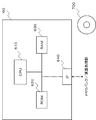
- FIG. 6 is a block diagram showing an example of the configuration of the data rearrangement unit 60 which is another configuration of the present embodiment.
- the data rearrangement unit 60 constitutes a computer including a CPU 610, a ROM 620, a RAM 630, and an IF 640.
- the CPU 610 reads a program from ROM 620.
- the CPU 610 controls the RAM 630 and the IF 640 based on the read program.
- the computer including the CPU 610 may realize each function as the input data selection unit 40, the multibank memory 41, and the rearrangement control unit 42 illustrated in FIG.
- the CPU 610 uses the RAM 630 as a temporary program storage when realizing each function.
- the CPU 610 may read a program included in the storage medium 700 that stores the program so as to be readable by a computer using a storage medium reading device (not shown). Alternatively, the CPU 610 may receive a program from an external device (not shown) via the IF 640.
- ROM 620 stores programs executed by CPU 610 and fixed data.
- the ROM 620 is, for example, a P-ROM (Programmable-ROM) or a flash ROM.
- the RAM 630 temporarily stores programs executed by the CPU 610 and data.
- the RAM 630 is, for example, a D-RAM (Dynamic-RAM).
- the IF 640 relays data exchange with the memory bank 30, the memory bank 33, the arithmetic processing unit 31, and the arithmetic processing unit 32.
- the IF 640 is a PCI (Peripheral Component Interconnect) card or a fiber channel card.
- the data rearrangement unit 60 configured in this way can obtain the same effects as the data rearrangement unit 34.
- the reason is that the CPU 610 of the data rearrangement unit 60 can realize the same operation as the data rearrangement unit 34 based on the program.
- the computing device 37 of the present embodiment operates in the same manner as in the first embodiment except that the rearrangement control of the data rearrangement unit 34 is different. Therefore, the description of the similar operation is omitted, and the operation unique to the present embodiment is described.
- the input data selection unit 40 selects input data to the arithmetic processing unit at the subsequent stage based on a signal for selecting input data supplied from the rearrangement control unit 42 of the data rearrangement unit 34, and Select whether to output the calculation result to the memory bank.
- the input data selection unit 40 of the data rearrangement unit 34 of the present embodiment inputs the input data as it is to the multi-bank memory 41.
- the input data selection unit 40 of this embodiment includes an arbitration mechanism that arbitrates the timing of data input when a situation occurs in which a plurality of data is simultaneously input to the same bank of the multi-bank memory 41.
- the arbitration mechanism of the present embodiment is not particularly limited.
- the arbitration mechanism may operate as follows.
- the arbitration mechanism receives the data. Then, the arbitration mechanism checks the input state of data to be output to the output destination (for example, port) of the data, that is, whether there is other data to be output.
- the arbitration mechanism If no other data is input, the arbitration mechanism outputs the received data to the output destination.
- the arbitration mechanism When other data is input, the arbitration mechanism outputs the data to be output first based on the instruction (parameter). Then, after the output data is received by the output destination and the output destination can receive the next data, the arbitration mechanism outputs the remaining data.
- the arbitration mechanism of the present embodiment may arbitrate data using a round robin method and sequentially write data one by one to the multi-bank memory 41.
- the computing device 37 can obtain an effect of reducing the operation of the rearrangement control unit 42.
- the input data selection unit 40 needs a circuit (mechanism) that holds parameters necessary for generation in order to generate an input data selection signal.
- the input data selection unit 40 of the arithmetic device 37 of the present embodiment includes an arbitration mechanism (circuit) for the timing of input data of the multi-bank memory 41.
- the circuit scale of the arbitration mechanism is smaller than the circuit scale for holding parameters. Therefore, the input data selection unit 40 of this embodiment can be realized with a smaller circuit scale than the input data selection unit 40 of the first embodiment.
- the computing device 37 of the present embodiment operates in the same manner as in the first embodiment except that the rearrangement control of the data rearrangement unit 34 is different. Therefore, the description of the similar operation is omitted, and the operation unique to the present embodiment is described.
- the rearrangement control unit 42 controls the read timing of the multi-bank memory 41 based on a counter for generating a write address to the input data selection unit 40. Based on this control, the rearrangement control unit 42 generates a predetermined delay in the calculation data transfer.
- the rearrangement control unit 42 of the present embodiment operates as follows.
- the rearrangement control unit 42 monitors the write address and read address of the multi-bank memory 41.
- the rearrangement control unit 42 operates as follows regarding data writing.
- the initial state of the multi-bank memory 41 is a state where all addresses are not written (unwritten).
- the rearrangement control unit 42 When the write address is “unwritten”, the rearrangement control unit 42 writes the data into the multi-bank memory 41. After writing, the rearrangement control unit 42 sets the address to “written”.
- the rearrangement control unit 42 stops writing to the multi-bank memory 41 until data at the address is read. Then, after the data at the address is read, the rearrangement control unit 42 writes the data at the address. In this case, the rearrangement control unit 42 sets the address as “already written”.
- the rearrangement control unit 42 operates as follows regarding reading.
- the rearrangement control unit 42 In the case of reading the “written” address, the rearrangement control unit 42 causes the multibank memory 41 to output the data stored in the read address. After the output, the rearrangement control unit 42 sets the address to “unwritten”.
- the rearrangement control unit 42 stops reading data until writing of the address is generated (becomes “written”).
- the rearrangement control unit 42 reads the data after detecting “written”.
- the rearrangement control unit 42 sets the address to “unwritten” after reading.
- rearrangement control unit 42 may set “unwritten / written” after confirming the presence / absence of writing to the address without setting “unwritten” after data reading.
- the rearrangement control unit 42 rearranges the data in the multi-bank memory 41 in the time direction and the output (port) direction.
- the arithmetic device 37 of the present embodiment can obtain an effect of facilitating control compared to the arithmetic device 37 of the first embodiment.
- the reordering control unit 42 of the arithmetic device 37 monitors the write address and read address of the multi-bank memory 41 and controls based on the address. Therefore, the rearrangement control unit 42 does not need to consider the timing of memory access in writing.
- First data storage means for storing calculation target data;
- An arithmetic processing means for performing an arithmetic operation using data;
- the instruction data is selected from the calculation target data stored in the first data storage means and the data calculated by the calculation processing means, and a delay instruction is specified among the specified data based on the parameters.
- a predetermined delay is given to the received data, the data not receiving the delay instruction is not delayed, the instructed data is rearranged based on the parameters, and is calculated by the arithmetic processing means.
- Data rearrangement means for outputting data and calculation result data of the calculation processing means;
- a second data storage means for storing the calculation result data output by the data rearranging means.
- the data rearranging means is The arithmetic unit according to claim 1, wherein the data to be instructed is selected from the arithmetic target data and data of arithmetic results of one or more arithmetic processing means.
- the data rearranging means includes: Input data selection means for receiving data, selecting the instructed data, and outputting to the second data storage means or the arithmetic processing means; Data is received from the input data selection means, based on the parameter, a delay is given to the data that has received a delay instruction, and the data that does not receive a delay instruction is not delayed, and is instructed based on the parameter Multi-port storage means for executing rearrangement and outputting from a predetermined output port;
- the arithmetic unit according to claim 1 or 2, further comprising: a rearrangement control unit that controls the input data selection unit and the multiport storage unit.
- the input data selection means is Check if there is other data with the same output destination as the input data. If there is no other data, output the input data. If there is other data, output any data. Thereafter, after the output destination becomes receivable again, the remaining data is output.
- the said rearrangement control means is Monitoring the read and write addresses of the multiport storage means; When a read instruction is received, If the read instruction address is already written, data is read from the read address, The arithmetic unit according to appendix 3 or appendix 4, wherein when the read instruction address is unwritten, the readout is stopped until data is written to the read address.
- (Appendix 6) Stores data to be calculated, Calculate using data, The selected data is selected from the stored calculation target data and the calculated data, and based on the parameters, a predetermined delay is given to the data that has received a delay instruction among the specified data, and the delay Without delaying the data that does not receive the instruction, the rearrangement of the specified data is executed based on the parameters, the calculated data and the calculation result data are output, A calculation method for storing the calculation result data.
- (Supplementary note 7) Processing for storing calculation target data; Processing using data, The selected data is selected from the stored calculation target data and the calculated data, and based on the parameters, a predetermined delay is given to the data that has received a delay instruction among the specified data, and the delay Processing that outputs the data to be calculated and the calculation result data by performing the rearrangement of the specified data based on the parameters without delaying the data not receiving the instruction;
- a computer-readable recording medium having recorded thereon a program for causing a computer to execute processing for storing the calculation result data.
- the present invention can be applied to processing for which the array processor is useful, that is, signal processing applications such as matrix operation, filtering processing, and data rearrangement.
Landscapes
- Engineering & Computer Science (AREA)
- Theoretical Computer Science (AREA)
- Physics & Mathematics (AREA)
- General Engineering & Computer Science (AREA)
- General Physics & Mathematics (AREA)
- Software Systems (AREA)
- Computer Hardware Design (AREA)
- Human Computer Interaction (AREA)
- Computing Systems (AREA)
- Advance Control (AREA)
- Executing Machine-Instructions (AREA)
- Multi Processors (AREA)
Abstract
Priority Applications (3)
| Application Number | Priority Date | Filing Date | Title |
|---|---|---|---|
| EP13867312.4A EP2940594A4 (fr) | 2012-12-25 | 2013-12-16 | Dispositif de calcul et procédé de calcul |
| JP2014554119A JP6432348B2 (ja) | 2012-12-25 | 2013-12-16 | 演算装置及び演算方法 |
| US14/654,876 US9507541B2 (en) | 2012-12-25 | 2013-12-16 | Computation device, computation method, and medium |
Applications Claiming Priority (2)
| Application Number | Priority Date | Filing Date | Title |
|---|---|---|---|
| JP2012281060 | 2012-12-25 | ||
| JP2012-281060 | 2012-12-25 |
Publications (1)
| Publication Number | Publication Date |
|---|---|
| WO2014103235A1 true WO2014103235A1 (fr) | 2014-07-03 |
Family
ID=51020359
Family Applications (1)
| Application Number | Title | Priority Date | Filing Date |
|---|---|---|---|
| PCT/JP2013/007383 Ceased WO2014103235A1 (fr) | 2012-12-25 | 2013-12-16 | Dispositif de calcul et procédé de calcul |
Country Status (4)
| Country | Link |
|---|---|
| US (1) | US9507541B2 (fr) |
| EP (1) | EP2940594A4 (fr) |
| JP (1) | JP6432348B2 (fr) |
| WO (1) | WO2014103235A1 (fr) |
Families Citing this family (2)
| Publication number | Priority date | Publication date | Assignee | Title |
|---|---|---|---|---|
| CN106126124B (zh) * | 2016-06-29 | 2019-05-21 | 北京联想核芯科技有限公司 | 一种数据处理方法及电子设备 |
| CN106484326B (zh) * | 2016-09-14 | 2019-08-27 | Oppo广东移动通信有限公司 | 一种数据传输处理方法及移动终端 |
Citations (8)
| Publication number | Priority date | Publication date | Assignee | Title |
|---|---|---|---|---|
| JPS5818116A (ja) | 1981-07-10 | 1983-02-02 | ル−カス・インダストリイズ・ピ−エルシ− | 誘導性トランスデユ−サ装置 |
| JPH04503720A (ja) | 1988-08-04 | 1992-07-02 | アレイ・マイクロシステムズ・インコーポレーテッド | デジタル信号処理装置のフレキシブル制御装置及び方法 |
| JP2002215603A (ja) * | 2001-01-19 | 2002-08-02 | Sony Corp | 演算装置および並列演算装置 |
| JP2006031127A (ja) * | 2004-07-12 | 2006-02-02 | Fujitsu Ltd | 再構成可能な演算装置 |
| JP2009282781A (ja) * | 2008-05-22 | 2009-12-03 | Canon Inc | 情報処理方法及び装置 |
| JP2010009247A (ja) * | 2008-06-25 | 2010-01-14 | Toshiba Corp | 半導体装置、および、半導体装置によるデータ処理方法 |
| JP2010117806A (ja) * | 2008-11-12 | 2010-05-27 | Toshiba Corp | 半導体装置、および、半導体装置によるデータ処理方法 |
| WO2011036918A1 (fr) * | 2009-09-24 | 2011-03-31 | 日本電気株式会社 | Circuit de réarrangement de données, circuit à retard variable, circuit à transformée de fourier à haut débit et procédé de réarrangement de données |
Family Cites Families (14)
| Publication number | Priority date | Publication date | Assignee | Title |
|---|---|---|---|---|
| JPS58181168A (ja) | 1982-04-17 | 1983-10-22 | Nippon Telegr & Teleph Corp <Ntt> | 自律型プロセツサアレイ方式 |
| JPH1091442A (ja) * | 1996-09-13 | 1998-04-10 | Hitachi Ltd | プロセッサ |
| JP3668356B2 (ja) * | 1997-04-07 | 2005-07-06 | シャープ株式会社 | 高速フーリエ変換演算回路 |
| JPH1185463A (ja) * | 1997-09-01 | 1999-03-30 | Mitsubishi Electric Corp | 演算ネットワーク装置 |
| JP4436951B2 (ja) * | 1999-12-22 | 2010-03-24 | パナソニック株式会社 | 信号処理系統設定装置及び方法 |
| US7020673B2 (en) | 2001-01-19 | 2006-03-28 | Sony Corporation | Reconfigurable arithmetic device and arithmetic system including that arithmetic device and address generation device and interleave device applicable to arithmetic system |
| TWI234737B (en) | 2001-05-24 | 2005-06-21 | Ip Flex Inc | Integrated circuit device |
| US7219172B1 (en) * | 2004-06-01 | 2007-05-15 | Storage Technology Corporation | System and method of dynamically controlling storage device access duty cycle |
| US7546434B2 (en) * | 2005-06-22 | 2009-06-09 | International Business Machines Corporation | Method to write data to an information storage and retrieval system |
| WO2007003370A2 (fr) * | 2005-06-30 | 2007-01-11 | Interuniversitair Microelektronica Centrum Vzw | Agencement memoire pour systemes multiprocesseurs |
| JP5163332B2 (ja) * | 2008-07-15 | 2013-03-13 | 富士通セミコンダクター株式会社 | 設計プログラム、設計装置、および設計方法 |
| JP5556323B2 (ja) * | 2010-04-15 | 2014-07-23 | 日本電気株式会社 | データ並び替え回路に対する制御情報自動生成方法、データ並び替え回路、コンピュータ、及び制御情報自動生成プログラム |
| US8738880B2 (en) * | 2010-08-17 | 2014-05-27 | International Business Machines Corporation | Throttling storage initialization for data destage |
| WO2013102970A1 (fr) * | 2012-01-04 | 2013-07-11 | 日本電気株式会社 | Dispositif et procédé de traitement de données |
-
2013
- 2013-12-16 US US14/654,876 patent/US9507541B2/en active Active
- 2013-12-16 JP JP2014554119A patent/JP6432348B2/ja active Active
- 2013-12-16 EP EP13867312.4A patent/EP2940594A4/fr not_active Ceased
- 2013-12-16 WO PCT/JP2013/007383 patent/WO2014103235A1/fr not_active Ceased
Patent Citations (8)
| Publication number | Priority date | Publication date | Assignee | Title |
|---|---|---|---|---|
| JPS5818116A (ja) | 1981-07-10 | 1983-02-02 | ル−カス・インダストリイズ・ピ−エルシ− | 誘導性トランスデユ−サ装置 |
| JPH04503720A (ja) | 1988-08-04 | 1992-07-02 | アレイ・マイクロシステムズ・インコーポレーテッド | デジタル信号処理装置のフレキシブル制御装置及び方法 |
| JP2002215603A (ja) * | 2001-01-19 | 2002-08-02 | Sony Corp | 演算装置および並列演算装置 |
| JP2006031127A (ja) * | 2004-07-12 | 2006-02-02 | Fujitsu Ltd | 再構成可能な演算装置 |
| JP2009282781A (ja) * | 2008-05-22 | 2009-12-03 | Canon Inc | 情報処理方法及び装置 |
| JP2010009247A (ja) * | 2008-06-25 | 2010-01-14 | Toshiba Corp | 半導体装置、および、半導体装置によるデータ処理方法 |
| JP2010117806A (ja) * | 2008-11-12 | 2010-05-27 | Toshiba Corp | 半導体装置、および、半導体装置によるデータ処理方法 |
| WO2011036918A1 (fr) * | 2009-09-24 | 2011-03-31 | 日本電気株式会社 | Circuit de réarrangement de données, circuit à retard variable, circuit à transformée de fourier à haut débit et procédé de réarrangement de données |
Also Published As
| Publication number | Publication date |
|---|---|
| EP2940594A1 (fr) | 2015-11-04 |
| JP6432348B2 (ja) | 2018-12-05 |
| EP2940594A4 (fr) | 2016-09-21 |
| US20150347056A1 (en) | 2015-12-03 |
| JPWO2014103235A1 (ja) | 2017-01-12 |
| US9507541B2 (en) | 2016-11-29 |
Similar Documents
| Publication | Publication Date | Title |
|---|---|---|
| CN103221935B (zh) | 从simd寄存器文件向通用寄存器文件移动数据的方法和装置 | |
| US9207995B2 (en) | Mechanism to speed-up multithreaded execution by register file write port reallocation | |
| JP2008507034A5 (fr) | ||
| US10824423B2 (en) | Computer system including reconfigurable arithmetic device with network of processor elements | |
| JP6432348B2 (ja) | 演算装置及び演算方法 | |
| US9747232B2 (en) | Data processing device | |
| EP1035479A2 (fr) | Système de traitement de données vectorielles | |
| US8560784B2 (en) | Memory control device and method | |
| JP6294732B2 (ja) | データ転送制御装置及びメモリ内蔵装置 | |
| CN102184090B (zh) | 一种动态可重构处理器及其固定数的调用方法 | |
| US11972263B2 (en) | Cooperative instruction prefetch on multicore system | |
| EP4320514B1 (fr) | Pré-extraction d'instructions coopératives sur un système multicoeur | |
| US20230153261A1 (en) | Processor and arithmetic processing method | |
| US20100318767A1 (en) | Multiplexing auxiliary processing element and semiconductor integrated circuit | |
| US20100064115A1 (en) | Vector processing unit | |
| JP2010049511A (ja) | 共有メモリへのアクセス方式およびマルチcpu構成のプログラマブルコントローラ | |
| US20150278095A1 (en) | Data processing device | |
| US7370158B2 (en) | SIMD process with multi-port memory unit comprising single-port memories | |
| WO2013102970A1 (fr) | Dispositif et procédé de traitement de données | |
| CN106716336A (zh) | 在多处理器系统中的存储器管理 | |
| JP2021064270A (ja) | 半導体装置およびその制御方法 | |
| JP4347352B2 (ja) | ベクトルデータ処理装置 | |
| JP2008102599A (ja) | プロセッサ | |
| JP2006338511A (ja) | 数値制御装置 | |
| US20170206180A1 (en) | Processor and data transfer method |
Legal Events
| Date | Code | Title | Description |
|---|---|---|---|
| 121 | Ep: the epo has been informed by wipo that ep was designated in this application |
Ref document number: 13867312 Country of ref document: EP Kind code of ref document: A1 |
|
| WWE | Wipo information: entry into national phase |
Ref document number: 2013867312 Country of ref document: EP |
|
| ENP | Entry into the national phase |
Ref document number: 2014554119 Country of ref document: JP Kind code of ref document: A |
|
| WWE | Wipo information: entry into national phase |
Ref document number: 14654876 Country of ref document: US |
|
| NENP | Non-entry into the national phase |
Ref country code: DE |