WO2014103254A1 - Dispositif de retrait d'organisme volant, électrode de piégeage et élément d'électrode de piégeage associé, et procédé de fabrication associé - Google Patents
Dispositif de retrait d'organisme volant, électrode de piégeage et élément d'électrode de piégeage associé, et procédé de fabrication associé Download PDFInfo
- Publication number
- WO2014103254A1 WO2014103254A1 PCT/JP2013/007455 JP2013007455W WO2014103254A1 WO 2014103254 A1 WO2014103254 A1 WO 2014103254A1 JP 2013007455 W JP2013007455 W JP 2013007455W WO 2014103254 A1 WO2014103254 A1 WO 2014103254A1
- Authority
- WO
- WIPO (PCT)
- Prior art keywords
- capture electrode
- capture
- electrode member
- resin
- electrode
- Prior art date
- Legal status (The legal status is an assumption and is not a legal conclusion. Google has not performed a legal analysis and makes no representation as to the accuracy of the status listed.)
- Ceased
Links
Images


Classifications
-
- A—HUMAN NECESSITIES
- A01—AGRICULTURE; FORESTRY; ANIMAL HUSBANDRY; HUNTING; TRAPPING; FISHING
- A01M—CATCHING, TRAPPING OR SCARING OF ANIMALS; APPARATUS FOR THE DESTRUCTION OF NOXIOUS ANIMALS OR NOXIOUS PLANTS
- A01M1/00—Stationary means for catching or killing insects
- A01M1/22—Killing insects by electric means
-
- B—PERFORMING OPERATIONS; TRANSPORTING
- B03—SEPARATION OF SOLID MATERIALS USING LIQUIDS OR USING PNEUMATIC TABLES OR JIGS; MAGNETIC OR ELECTROSTATIC SEPARATION OF SOLID MATERIALS FROM SOLID MATERIALS OR FLUIDS; SEPARATION BY HIGH-VOLTAGE ELECTRIC FIELDS
- B03C—MAGNETIC OR ELECTROSTATIC SEPARATION OF SOLID MATERIALS FROM SOLID MATERIALS OR FLUIDS; SEPARATION BY HIGH-VOLTAGE ELECTRIC FIELDS
- B03C3/00—Separating dispersed particles from gases or vapour, e.g. air, by electrostatic effect
- B03C3/34—Constructional details or accessories or operation thereof
- B03C3/40—Electrode constructions
- B03C3/45—Collecting-electrodes
- B03C3/47—Collecting-electrodes flat, e.g. plates, discs, gratings
-
- B—PERFORMING OPERATIONS; TRANSPORTING
- B03—SEPARATION OF SOLID MATERIALS USING LIQUIDS OR USING PNEUMATIC TABLES OR JIGS; MAGNETIC OR ELECTROSTATIC SEPARATION OF SOLID MATERIALS FROM SOLID MATERIALS OR FLUIDS; SEPARATION BY HIGH-VOLTAGE ELECTRIC FIELDS
- B03C—MAGNETIC OR ELECTROSTATIC SEPARATION OF SOLID MATERIALS FROM SOLID MATERIALS OR FLUIDS; SEPARATION BY HIGH-VOLTAGE ELECTRIC FIELDS
- B03C3/00—Separating dispersed particles from gases or vapour, e.g. air, by electrostatic effect
- B03C3/34—Constructional details or accessories or operation thereof
- B03C3/40—Electrode constructions
- B03C3/60—Use of special materials other than liquids
- B03C3/64—Use of special materials other than liquids synthetic resins
Definitions
- the present invention prevents small organisms such as pollen and small frogs floating in the air (hereinafter collectively referred to as “flying organisms”) from entering the room on the flow of air such as ventilation.
- the present invention relates to a flying organism removing apparatus, a capture electrode thereof, a capture electrode member used for the capture electrode, and a manufacturing method thereof.
- an electric dust collector such as an air cleaner is often used as a method for removing pollen and dust in the interior space of factories, buildings, and houses.
- these electric dust collectors it is composed of a suction unit for sucking air, a charging unit (ionizer), a dust collection unit, a high voltage power supply unit, and a control unit.
- a charging unit ionizer
- a dust collection unit e.g., a dust collection collector
- a high voltage power supply unit e.g., a high voltage power supply unit
- a control unit e.g., a control unit.
- Such an electrostatic precipitator is an electrode plate to which a high voltage called a dust collection collector is applied, in which dust mixed in air sucked by a fan is charged in advance to a positive electrode by an ionizer located in the preceding stage, and kept in a subsequent stage. Designed to capture on the negative side.
- the negative electrode is made of a metal plate such as aluminum
- the positive electrode is made of a metal plate covered with an insulating resin or a semiconductive resin.
- the negative electrode is a metal foil or a metal-deposited resin film
- the positive electrode is a metal foil or a metal-deposited resin film covered with an insulating resin or a semiconductive resin.
- Patent Document 5 There is also a structure in which they are provided and stacked or wound (for example, see Patent Document 5). In many cases, these dust collectors are not coated with the metal on the negative electrode side.
- Japanese Patent No. 2547248 (5th page, 4th page, 6th page, 7th page) Japanese Patent No. 3346925 (page 7, FIG. 1, FIG. 4, FIG. 7, FIG. 8) Japanese Patent No. 3516725 (page 7, FIG. 2) Japanese Patent No. 4347837 (page 8, FIG. 4) JP-A-1-210049 (page 3, FIG. 2, page 4, FIG. 5) Japanese Patent No. 3559596 (page 7, Fig. 1) Japanese Patent Laid-Open No. 2003-180219 (page 6, FIG. 6)
- the surface of the dust collector was covered with an insulating material.
- a positive charge is accumulated on the negative electrode side, resulting in a phenomenon of weakening the electrostatic field. Therefore, in order to release the accumulated electric charge to the electrode side, it has been considered to cover the dust collector with an insulating material having a slightly reduced resistance value.
- the positive electrode (high voltage side) of the dust collector is a semiconductive resin having a volume resistivity of 10 10 to 10 15 ⁇ ⁇ cm or a surface resistivity of 10 10 to 10 14 ⁇ / ⁇ . If it is coated with, it will neutralize the charged dust adhering to the electrode surface over a long period of use, and prevent the dust collection rate from decreasing and the discharge and ignition when metal fine particles and oil droplets are mixed. It was supposed to be possible. However, actually, there are flying creatures that cannot be captured even if the volume resistivity or surface resistivity is in the above range.
- the volume resistivity is less than 10 7 ⁇ ⁇ cm, or the surface resistivity is less than 10 7 ⁇ / ⁇ , depending on the magnitude of the applied voltage, a spark discharge tends to occur toward the opposing metal electrode, and a short circuit occurs.
- an abnormality such as, the flowing current is large, so there is a risk that the electrode itself generates heat and may cause a fire.
- adhesive sheets and electric shock insect killers that use an attracting light such as ultraviolet rays are effective in capturing and killing insects, but the effect is limited only to the peripheral area where they are installed.
- a flying organism removing device is required.
- the present invention has been conceived in view of the above problems, and is capable of maintaining a stable surface potential over a long period of time. Moreover, even when the applied voltage is relatively low, the desired flying organism (insect) capture performance is exhibited.
- a safe flying organism removing apparatus that can perform discharge and that does not cause discharge, a capture electrode thereof, a capture electrode member constituting the capture electrode, and a method of manufacturing the capture electrode member.
- the capture electrode member of the present invention is A capture electrode member constituting the capture electrode of the flying organism removing apparatus, A conductive substrate; It has a semiconductive layer which coat
- the capture electrode of the present invention is characterized in that a pair of the capture electrode members are used, one being a positive electrode and the other being a negative electrode.
- the flying organism removing apparatus of the present invention is characterized by comprising the capture electrode and a power source for supplying a voltage to the capture electrode.
- the characteristics of the semiconductive layer covering the conductive substrate are such that the surface resistivity is 10 8 to 10 11 ⁇ / ⁇ and the volume resistivity is 10 8 to 10 11 ⁇ ⁇ cm.
- the surface resistivity is 10 8 to 10 11 ⁇ / ⁇
- the volume resistivity is 10 8 to 10 11 ⁇ ⁇ cm.
- the device itself can be reduced in size and power can be saved.
- the whole weight can be formed lightly by comprising a core material with a material whose specific gravity is lighter than metals, such as resin.
- the shape has a high degree of freedom, and shapes such as a rod shape, a sheet shape, and a mesh shape can be easily formed.
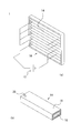
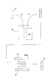
- FIG. 1 (a) shows a configuration example of the flying organism removing apparatus according to the present invention.
- the flying organism removing apparatus 1 includes at least a capture electrode 10 and a power source 12. In addition, parts such as a fan and an ionizer may be added.
- the capture electrodes 10 are arranged on the same plane with strip-shaped capture electrode members 14 aligned in directions, and are alternately connected to different polarities. Flying organisms are captured by the electrostatic field generated between the capture electrode members 14.
- FIG. 1B is a perspective view including a cross-sectional view of the capture electrode member 14.
- the capture electrode member 14 is covered with a semiconductive layer 18 around a conductive substrate 16 in the center.
- a terminal 20 that is electrically connected to the conductive substrate 16 is provided on at least one end side of both ends of the capture electrode member 14. The position of the terminal 20 is not particularly limited.
- the conductive substrate 16 desirably has at least an electric resistance of 10 1 ⁇ or less.
- the semiconductive layer 18 is basically formed of an insulating material, and has a surface resistivity of 10 8 to 10 11 ⁇ / ⁇ and a volume resistivity of 10 8 to 10 11 ⁇ ⁇ It is characterized by being cm. More preferably, the surface resistivity is 10 8 to 10 9 ⁇ / ⁇ , and the volume resistivity is 10 8 to 10 9 ⁇ ⁇ cm.
- both the surface resistivity and the volume resistivity are in this range, the charge accumulated on the surface of the semiconductive layer 18 can be transferred to the conductive substrate 16, and conversely from the conductive substrate 16 to the semiconductive layer. Since charges can also be transferred to the surface of the sex layer 18, it is possible to stably capture insects and pollen over a long period of time. Moreover, many kinds of flying organisms can be captured when both the resistivity values are within this range.
- the trapping force is reduced when the resistivity is high. Further, if the resistivity is low, a discharge occurs between the capture electrode members 14 or a large current flows when an abnormality such as a short circuit occurs, and the capture electrode member 14 itself generates heat, resulting in a risk of ignition.
- the conductive substrate 16, the semiconductive layer 18, the capture electrode member 14, and the capture electrode 10 will be described in order.
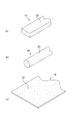
- the conductive substrate 16 is generally a metal, and has a rod shape (FIGS. 2 (a) and (b)) and a sheet shape (FIG. 2 (c)). Can be classified into the following shapes.
- the cross-sectional shape 22 is classified into a polygon (FIG. 2A) and a circle (FIG. 2B).
- the polygon may not be a regular polygon, and the circle may be an ellipse or a track shape (combination of arc and straight line).
- the ratio of the cross-sectional shape 22 to the length is not particularly limited.
- the conductive substrate 16 When the conductive substrate 16 is formed of a metal, it can be formed by a generally known method such as melting and extrusion from a die. Moreover, when producing with a thin film, methods, such as vacuum film-forming or plating, can be utilized.
- the core material 24 may be included in the center of these members.
- the core member 24 is desirably a substance (for example, resin) having a specific gravity lighter than that of metal.
- the core material 24 is used to reduce the total weight.
- the sheet-like core material 24 may be used as a substrate material, and a metal film may be formed on the surface thereof to form the conductive base material 16.
- a means for conducting the upper metal film 16a and the lower metal film 16b may be provided. This is because when the core member 24 is insulative, the metal film on the front side and the back side of the core member 24 is not conductive. Of course, when using without conducting, it is not necessary to conduct the metal film on the front side and the back side of the core member 24.
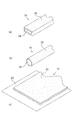
- FIG. 4 shows a case where the conductive substrate 16 is carbon fiber.
- the carbon fiber is electrically conductive, is light in weight, is formed while being coated with resin, and can be fired later to fix the shape, which is convenient.
- FIG. 4A is a plate shape
- FIG. 4B is a rod shape.
- the plate shape may be included in a rod shape.
- the plate-like conductive base material 16 can be obtained by bonding the carbon fiber sheet 30 knitted into a sheet shape.
- a plurality of carbon fibers 31 may be collected to obtain the conductive base material 16.
- thread-like carbon fibers 32 may be woven into a sheet shape. These carbon fibers can form a firm shape by forming a resin or applying a resin during formation and firing after forming.
- the carbon fiber includes a carbon fiber rod, a carbon fiber plate, a carbon fiber knitted fabric, a carbon fiber composite, and the like.
- FIG. 5 shows the conductive base material 16 when formed of a resin and a conductive filler 33.
- the resin may be thermosetting or thermoplastic.
- thermoplasticity it is desirable to select a resin having a high glass transition temperature.
- conductive carbon such as ketjen black or metal particles such as aluminum can be suitably used.
- the conductive filler 33 may be used by mixing a plurality of types. For example, in the case of using a thermosetting resin, the thermosetting resin is dissolved with a solvent or the like, and the conductive filler 33 is put in it and dispersed well. Thereafter, it is formed into a predetermined shape and heated to be cured.
- the powdered resin and the conductive filler 33 are well kneaded, heated and melted, formed into a predetermined shape, and cooled.
- the electrical resistance of the finished conductive substrate 16 is preferably 10 1 ⁇ or less.
- a core material 24 may be used. This is because the total weight is reduced.
- the electroconductive base material 16 shown here may be used individually, and may be used in combination of multiple types or multiple.
- the semiconductive layer 18 is a layer having a surface resistivity of 10 8 to 10 11 ⁇ / ⁇ and a volume resistivity of 10 8 to 10 11 ⁇ ⁇ cm, and is disposed around the conductive substrate 16. It is. In particular, it is more preferable that the surface resistivity is 10 8 to 10 9 ⁇ / ⁇ and the volume resistivity is 10 8 to 10 9 ⁇ ⁇ cm.
- the semiconductive layer 18 is an insulating layer, but the resistivity is not as high as that of a general insulating resin such as polypropylene, and the resistivity is not so low that it can be said to have conductivity. Just like an antistatic sheet, it is not completely conductive, but has a conductivity sufficient to allow the charged charge to flow through the conductive substrate 16.
- the semiconductive layer 18 is not particularly limited as long as it is within the above resistivity range. Some specific examples are shown below.
- Fig. 7 shows an example using water-based paint.
- the water-based paint is obtained by dissolving a resin (urethane or acrylic) in a solvent containing a hydroxyl group such as alcohol or glycol.
- a solution containing 5 to 20% of solvent (water-based paint) is prepared.
- water-based paints water-based urethane, water-based acrylic, etc.
- hydroxyl groups such as ethylene glycol monobutyl ether as a solvent component, and the hydroxyl groups remain even after drying, which facilitates the transfer of charges from the inside of the electrode to the surface of the coating material, and stabilizes insects and pollen. Can be captured. Further, glycerin having a hydroxyl group or the like may be added to increase the capturing power.
- the conductive substrate 16 formed in a predetermined shape is immersed in this solution (arrow 70). Then, it is pulled up (arrow 71). As a result, the conductive substrate 16 was coated with a solvent containing hydroxyl group and a resin. The conductive base material 16 coated with a solvent containing a hydroxyl group and a resin is then dried 73 to form the capture electrode member 14, but the solvent containing the hydroxyl group remains in this coating.
- acquisition electrode member 14 is continuously wound by immersing the sheet-like electroconductive base material 16 in the said solution, letting it pass through a drying furnace, and winding up. Can be obtained.
- the capture electrode member 14 Since the semiconductive layer 18 formed by this method is formed of a solvent containing a hydroxyl group remaining after drying and a resin, the capture electrode member 14 has a semiconductive layer on the surface of the conductive substrate 16. 18 is covered.
- the shape of the conductive substrate 16 is not limited.
- the rod-shaped conductive base material 16 is formed in a lattice shape or a mesh shape, it can be simply dipped in the solution and dried. This is because the semiconductive layer 18 can be formed.
- FIG. 8 shows a case where the semiconductive layer 18 is formed by injection molding.
- the thermoplastic resin 35 and the antistatic agent 36 are mixed. These particles preferably have a particle size of about several ⁇ m to several tens of ⁇ m. This is to facilitate later dispersion.
- the antistatic agent 36 carbon or metal powder can be preferably used.
- composition ratios may be determined so that the respective composition ratios are the values of the surface resistivity and the volume resistivity required for the semiconductive layer 18.
- the thermoplastic resin 35 is melted by heating, and further mixed and dispersed. This is because the antistatic agent 36 is uniformly dispersed.
- the mixture of the thermoplastic resin 35 and the antistatic agent 36 thus produced is referred to as “mixed resin 37”.
- FIG. 8 shows the mixed resin 37 formed in a cylindrical shape.
- the mixed resin 37 is injected into a sheet using an injection molding machine.
- the conductive base material 16 is covered with the obtained sheet-like semiconductive layer 18.
- only the periphery of the conductive substrate 16 may be attached with an adhesive, or a so-called laminating method in which welding is performed while removing air may be used.
- FIG. 8 shows a perspective view including a cross section of the capture electrode member 14 formed by the conductive base material 16 laminated with the semiconductive layer 18 to which both sides (14a, 14b) are bonded.
- a conductive base material 16 having a long rectangular shape with a flat cross section is sandwiched between semiconductive layers 18 wider than a width 16 w of the conductive base material 16.
- the upper and lower semiconductive layers 18 are bonded to each side (14a, 14b) by welding or the like.
- the upper and lower semiconductive layers 18 are preferably in a conductive state.
- FIG. 9 shows a case where the conductive base material 16m assembled in a mesh shape is sandwiched between the sheet-like semiconductive layers 18.
- the conductive base material 16m assembled in a mesh shape can be configured by assembling the rod-shaped conductive base material 16 shown in FIGS. 2 to 6 in a mesh shape.
- a laminating method can be used.
- FIG. 9B shows a state in which a net-like conductive base material 16m is sandwiched between the two sheet-like semiconductive layers 18 of FIG. 9A and the sheet-like semiconductive layers 18 are bonded to each other. Show.
- FIG. 9C shows a state where the through holes 19 are formed along the mesh.
- the through-hole 19 is formed by preparing a jig provided with a projection in a portion corresponding to the mesh in advance, and punching the sheet-like semiconductive layer 18 with this projection, so that the mesh-like capture electrode can be formed in one step.
- the member 14m can be obtained.
- FIG. 10 shows a case where the capture electrode member 14 is formed by attaching the material of the semiconductive layer 18 in a sol form to the conductive base material 16 and baking it.
- a liquid plasticizer represented by DOP (di-2-ethylhexyl phthalate) or the like is charged in the container 40.
- the vinyl chloride powder is added here and mixed.
- the powder of vinyl chloride is made sufficiently fine, it can be made into a sol based on a liquid plasticizer. This is referred to as a mixed resin sol 38.
- the conductive substrate 16 preheated in advance at about 300 ° C. is immersed (70) and pulled up (71).
- the conductive base material 16 to which the mixed resin sol 38 is adhered is heated using a heater 72 to form a vinyl chloride coating layer containing a plasticizer on the surface of the conductive base material 16.
- This coating layer becomes the semiconductive layer 18.
- a material having a high melting point is preferably used as the conductive base material 16 for preheating.
- This coating layer preferably contains 20 to 45% of DOP.
- a liquid plasticizer typified by DOP (di-2-ethylhexyl phthalate) and the like can be present between particles of vinyl chloride, which is an electrically insulating composition, to enable charge transfer, and from inside the electrode. It is easy to transfer charges to the surface of the coating resin, and insects and pollen can be captured stably.
- the capture electrode member 14 thus obtained can form the semiconductive layer 18 regardless of the shape of the conductive substrate 16.
- ⁇ Capture electrode 10> The capture electrode 10 produced with the capture electrode member 14 formed as described above will be described. A shape other than the capture electrode 10 shown in FIG. 1 will be described.
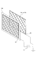
- FIG. 11 shows a case where the capture electrode member 14 has a mesh shape.
- the capture electrode member 14m is formed by coating a semiconductive layer 18 on a net-like conductive base material 16m. This is referred to as a net-like capture electrode member 14m.
- a mesh is formed on the frame 13 with the rod-like conductive base material 16 (in this state, the mesh-like conductive base material 16m), and this is used. It is formed by immersing in the material of the semiconductive layer 18 (see FIGS. 7 and 10).
- the frame body 13 may not be provided.
- mesh-like capture electrode members 14m are fixed with their surfaces facing each other. A fixing holder is not shown. At that time, the respective net-like capture electrode members 14m are insulated from each other. Then, terminals 20 are formed on each mesh-shaped capture electrode member 14m, and one mesh-shaped capture electrode member 14m is a positive electrode, and the other mesh-shaped capture electrode member 14m is a negative electrode. For safety reasons, it is desirable to ground either the positive electrode side or the negative electrode side.
- the capture electrode 10 can be formed with such a configuration. An electrostatic field is formed between the surfaces of the capture electrodes 10 facing each other. Further, the flying organism removing apparatus 1 is obtained by connecting the power source 12 to the capture electrode 10.
- FIG. 12 (a) shows a perspective view of another form of the mesh-like capturing electrode member 14m.
- the mesh-shaped capture electrode member 14m is obtained by wrapping a mesh-shaped conductive base material 16m with a sheet-like semiconductive layer 18 and opening through holes 19 in the mesh portion (see FIG. 9).
- FIG. 12B shows a cross-sectional view of the net-like capture electrode member 14m taken along the line AA in FIG.
- a sheet-like semiconductive layer 18 is wrapped from both sides of a rod-shaped conductive substrate 16 assembled in a mesh shape.
- the through-hole 19 can be formed by a punch that can be perforated through holes that have been aligned in advance. Therefore, compared with the case where the semiconductive layer 18 is formed by immersing the mesh-like conductive base material 16m in the paint-like semiconductive layer 18, the tact time at the time of manufacture is not much longer than the time for drying. There is a merit that it is short.
- each mesh-shaped capture electrode member 14m is opposed to each other.
- the capture electrode 10 can be formed by connecting the power source 12 between the members 14m.
- the mesh-like capture electrode member 14m shown in FIG. 12A and the mesh-like conductive substrate 16m or the mesh-like conductive substrate 16m shown in FIG. 11 are coated.
- the mesh-shaped capture electrode member 14m may be arranged to face each other.
- the mesh-shaped capture electrode member 14 m may be connected to one pole of the power supply 12 alone to constitute the capture electrode 10. This is because a small flying creature can be captured by the mesh-like capture electrode 10 alone.
- the counter electrode of the mesh-shaped capture electrode member 14m is a ground plane. Therefore, the case when the flying organism removing apparatus 1 is assembled is a counter electrode.
- the mesh-like capture electrode member 14m does not need to be fixed, and therefore may be in a flexible state without the frame 13. That is, air passes through the through hole 19, but the flying creatures are captured and can be used like a curtain.
- FIG. 15 (a) shows variations of the grid-like capture electrode 10 and flying organism removal apparatus 1 shown in FIG. 1 and the capture electrode member 14 that can be used therefor.
- the capture electrode member 14 is used in a portion that hits a lattice-like lattice.
- FIG. 15B shows the capture electrode member 14 in which the metal layer 23 is provided around the core member 24, the conductive base material 16 is formed, and the semiconductive layer 18 is formed around the periphery with a water-based paint.
- the core material 24 is made of resin, and the surrounding metal layer 23 is formed by plating a CrNi (chromium / nickel) alloy and covered with a water-soluble urethane paint.
- the semiconductive layer 18 is used.
- FIG. 15C shows a capture electrode member 14 in which a good conductor such as a metal foil, a carbon fiber sheet, or a conductive rubber plate is used as the conductive base material 16 and the periphery thereof is covered with a resin sheet.
- the semiconductive layer 18 is composed of two thermoplastic vinyl chlorides. That is, the capture electrode member 14 is laminated with two sheets of vinyl chloride (see FIG. 8).
- FIG. 15 (d) shows a case where the semiconductive layer 18 in which a thermoplastic resin and DOP (liquid plasticizer) are mixed is formed around the conductive substrate 16 as a metal wire.
- a preheated metal wire is immersed in a sol-like mixture of a thermoplastic resin and DOP that are previously molded in a fine powder form, and the sol is attached around the metal wire. Thereafter, heat treatment is performed to form a semiconductive layer 18 around the metal (see FIG. 10).
- FIG. 16 shows a sheet-like capturing electrode 10 formed by winding a pair of holding electrodes 10 while maintaining a predetermined interval.
- FIG. 16A shows the configuration of the capture electrode 10 and the flying organism removing apparatus 1 using the same.
- the capture electrode member 14 is formed by forming a semiconductive layer 18 on a sheet-like conductive substrate 16. The surfaces of the pair of capture electrode members 14 are opposed to each other and wound together with a holding member for holding a predetermined interval. Each of the wound capture electrode members 14 is connected to the positive electrode and the negative electrode.
- the trapping electrode 10 that is wound into a cylindrical shape allows air to flow from the top surface to the bottom surface of the tube, and traps flying creatures.
- FIG. 16B shows a view of the capture electrode 10 in which a mountain-shaped buffer member 27 is wound between the pair of capture electrode members 14 as viewed from the upper surface side.
- the buffer member 27 can be preferably made of an insulating material.
- the buffer member 27 desirably has a higher resistivity than the semiconductive layer 18.
- FIG. 16C shows a case where a buffer stand 28 is provided between the capture electrode members 14.
- FIG. 16D illustrates the capture electrode member 14 provided with a buffer stand 28.
- the buffer stand 28 is a block-shaped protrusion formed on the semiconductive layer 18 of the capture electrode member 14.
- the buffer electrode 28 can be disposed and bonded on at least one surface.
- a normal adhesive may be used for the adhesion.
- Providing the buffer stand 28 in this manner is preferable because a wide area of the capture electrode member 14 can be used for capturing flying creatures.
- a semiconductive layer 18 was formed on a conductive base 16 made of an iron flat plate having a width of 20 mm, a length of 100 mm, and a thickness of 1 mm.
- the material constituting the semiconductive layer 18 is water urethane, water acrylic, oil urethane, oil acrylic, ABS resin mixed with 30% carbon powder, ABS resin mixed with 5% carbon powder.
- Vinyl chloride (PVC) mixed with 35% DOP and PVC mixed with 10% DOP were used.
- a PP (polypropylene) film was used as a comparative example was prepared. Each surface resistivity and volume resistivity are shown in Table 1.
- the pair of capture electrode members 14 thus produced were opposed to each other and fixed so that the distance was 3 mm. Then, a DC voltage of ⁇ 2000 V was applied between the respective capture electrode members 14.
- the double circle is a state in which insects are strongly captured and the captured insects are not separated even when a wind of about 2 m / s is blown.
- the circle is in a state where insects are captured but is separated from the capture electrode member 14 by a wind having a wind speed of about 2 m / s.
- the triangle is a state in which insects are trapped but separated from the trapping electrode member 14 by wind at a wind speed of about 1 m / s.
- X is a state where no insects were captured.
- Drosophila could not capture Sample 3, Sample 4, Sample 6, Sample 8, and Sample 9 whose volume resistivity exceeded 10 12 ⁇ ⁇ cm. Further, Sample 6 and Sample 9 having a surface resistivity exceeding 10 12 ⁇ / ⁇ could not capture tobacco whitefly.
- Samples 1, 2, 5, and 7 having surface resistivity of 10 8 to 10 11 ⁇ / ⁇ and volume resistivity of 10 8 to 10 11 ⁇ ⁇ cm should capture any insects. I was able to. In particular, Samples 1 and 2 had very high capture power. These samples 1, 2, 5, and 7 are the capture electrodes 10 constituted by the capture electrode member 14 according to the present invention.
- the suitable flying organism removal apparatus 1 can be obtained.
- the surface resistivity of 10 8 to 10 9 ⁇ / ⁇ and the volume resistivity of 10 8 to 10 9 ⁇ ⁇ cm are most preferable.
- the flying organism removing apparatus using the capture electrode according to the present invention can be suitably used for an air intake hole of a building, and is also suitably used for a ventilation means including a warehouse, a barn, a window of a house, and an intake of an air conditioner. can do.
- Capture electrode 12 Power supply 13 Frame 14
- Capture electrode member 14a, 14b 14m of both sides Mesh-like capture electrode member 16
- Conductive base material 16a Upper metal film 16b Lower metal film 16m Mesh-like conductive group Material 18
- Semiconductive layer 19 Through-hole 20
- Terminal 22 Cross-sectional shape 24
- Core material 27 Buffer member 28
- Buffer stand 30 Carbon fiber sheet 31
- Carbon fiber 32 Threaded carbon fiber 33
- Conductive filler 38 Mixed resin sol 70 Dipping 71 Lifting 72 Heater 73 Dry
Landscapes
- Life Sciences & Earth Sciences (AREA)
- Pest Control & Pesticides (AREA)
- Engineering & Computer Science (AREA)
- Insects & Arthropods (AREA)
- Wood Science & Technology (AREA)
- Zoology (AREA)
- Environmental Sciences (AREA)
- Catching Or Destruction (AREA)
- Electrostatic Separation (AREA)
Abstract
Selon l'invention, dans des collecteurs de poussière électriques et des dispositifs de retrait d'organisme volant, des matériaux de base conducteurs sur lesquels des tensions élevées sont appliquées sont recouverts par une résine isolante pour éviter une décharge d'arc. Mais il existait le problème qu'en cas d'utilisation prolongée, une charge soit accumulée sur la surface d'électrode, ce qui réduit les capacités de collecte de poussière ou les capacités de piégeage. De plus, étant donné que l'électrode conductrice était configurée à partir d'un métal, il existait les problèmes de poids augmenté pour de grosses pièces et le travail énorme nécessaire lors de l'installation du transport de celles-ci. Le recouvrement d'au moins l'un des matériaux de base conducteurs avec une couche semi-conductrice ayant une résistive de surface de 108 à 1011 Ω/□ et une résistivité volumique de 108 à 1011 Ω/cm fournit une électrode qui ne subit pas de décharge d'arc, qui n'accumule pas de charge sur la surface d'électrode, et pour laquelle une performance de piégeage ne diminue pas avec une utilisation prolongée. L'utilisation d'un plaquage de métal, etc., sur la surface d'une pièce moulée en résine, etc., en tant que structure du matériau de base conducteur permet de rendre possible une réduction de poids tout en maintenant des propriétés d'alimentation en courant qui sont équivalentes à un métal.
Applications Claiming Priority (2)
| Application Number | Priority Date | Filing Date | Title |
|---|---|---|---|
| JP2012-286529 | 2012-12-28 | ||
| JP2012286529A JP2014128203A (ja) | 2012-12-28 | 2012-12-28 | 飛動生物除去装置とその捕捉電極及び捕捉電極部材とその製造方法 |
Publications (1)
| Publication Number | Publication Date |
|---|---|
| WO2014103254A1 true WO2014103254A1 (fr) | 2014-07-03 |
Family
ID=51020375
Family Applications (1)
| Application Number | Title | Priority Date | Filing Date |
|---|---|---|---|
| PCT/JP2013/007455 Ceased WO2014103254A1 (fr) | 2012-12-28 | 2013-12-19 | Dispositif de retrait d'organisme volant, électrode de piégeage et élément d'électrode de piégeage associé, et procédé de fabrication associé |
Country Status (2)
| Country | Link |
|---|---|
| JP (1) | JP2014128203A (fr) |
| WO (1) | WO2014103254A1 (fr) |
Cited By (2)
| Publication number | Priority date | Publication date | Assignee | Title |
|---|---|---|---|---|
| CN116713114A (zh) * | 2023-08-08 | 2023-09-08 | 江苏中顺节能科技有限公司 | 一种液膜均布的湿式电除尘器收尘极板及液膜分布方法 |
| CN116764815A (zh) * | 2023-07-12 | 2023-09-19 | 山东雪圣环境工程有限公司 | 静电除尘过滤器及应用于静电除尘过滤器中的电极板 |
Families Citing this family (5)
| Publication number | Priority date | Publication date | Assignee | Title |
|---|---|---|---|---|
| JP6713620B2 (ja) * | 2015-02-20 | 2020-06-24 | 学校法人近畿大学 | 静電場発生装置、飛動生物除去装置及び植物保護装置 |
| TWI690367B (zh) * | 2015-09-09 | 2020-04-11 | 日商創意科技股份有限公司 | 空氣清淨機 |
| JP6718846B2 (ja) * | 2017-07-11 | 2020-07-08 | アース環境サービス株式会社 | 花粉粒捕捉装置 |
| JP6469200B1 (ja) * | 2017-11-07 | 2019-02-13 | 株式会社昭栄 | 捕虫器 |
| KR102660384B1 (ko) * | 2021-09-01 | 2024-04-24 | 김준석 | 정전집진장치 |
Citations (13)
| Publication number | Priority date | Publication date | Assignee | Title |
|---|---|---|---|---|
| JPS62206082A (ja) * | 1986-03-01 | 1987-09-10 | 株式会社 松井色素化学工業所 | 線状体の製造方法 |
| JPS63176558U (fr) * | 1987-04-09 | 1988-11-16 | ||
| JPH05146715A (ja) * | 1991-11-29 | 1993-06-15 | Matsushita Electric Ind Co Ltd | 電気集塵機の集塵部電極 |
| JPH10156214A (ja) * | 1996-11-28 | 1998-06-16 | Matsushita Seiko Co Ltd | 水蒸気の回収装置 |
| JP2000325830A (ja) * | 1999-01-22 | 2000-11-28 | Sanyo Electric Co Ltd | 空気清浄機用放電電極 |
| JP2002095996A (ja) * | 2000-09-21 | 2002-04-02 | Mitsubishi Electric Corp | 空気浄化装置 |
| JP2008018340A (ja) * | 2006-07-13 | 2008-01-31 | Trinc:Kk | 浮遊物捕捉装置および浮遊物反発装置 |
| JP2008062173A (ja) * | 2006-09-07 | 2008-03-21 | Matsushita Electric Ind Co Ltd | 集塵装置および空調装置 |
| JP2008183540A (ja) * | 2007-01-31 | 2008-08-14 | Mitsubishi Electric Corp | 電気集塵デバイス |
| JP2008284515A (ja) * | 2007-05-21 | 2008-11-27 | Daicel Polymer Ltd | 集塵エレメント用部材及び集塵エレメント |
| JP2010094635A (ja) * | 2008-10-17 | 2010-04-30 | Midori Anzen Co Ltd | 電気集塵機 |
| JP2010227833A (ja) * | 2009-03-27 | 2010-10-14 | Panasonic Corp | 集塵装置 |
| JP2010279270A (ja) * | 2009-06-03 | 2010-12-16 | Navec Co Ltd | 静電場発生装置及びそれを用いた飛動生物除去方法 |
-
2012
- 2012-12-28 JP JP2012286529A patent/JP2014128203A/ja active Pending
-
2013
- 2013-12-19 WO PCT/JP2013/007455 patent/WO2014103254A1/fr not_active Ceased
Patent Citations (13)
| Publication number | Priority date | Publication date | Assignee | Title |
|---|---|---|---|---|
| JPS62206082A (ja) * | 1986-03-01 | 1987-09-10 | 株式会社 松井色素化学工業所 | 線状体の製造方法 |
| JPS63176558U (fr) * | 1987-04-09 | 1988-11-16 | ||
| JPH05146715A (ja) * | 1991-11-29 | 1993-06-15 | Matsushita Electric Ind Co Ltd | 電気集塵機の集塵部電極 |
| JPH10156214A (ja) * | 1996-11-28 | 1998-06-16 | Matsushita Seiko Co Ltd | 水蒸気の回収装置 |
| JP2000325830A (ja) * | 1999-01-22 | 2000-11-28 | Sanyo Electric Co Ltd | 空気清浄機用放電電極 |
| JP2002095996A (ja) * | 2000-09-21 | 2002-04-02 | Mitsubishi Electric Corp | 空気浄化装置 |
| JP2008018340A (ja) * | 2006-07-13 | 2008-01-31 | Trinc:Kk | 浮遊物捕捉装置および浮遊物反発装置 |
| JP2008062173A (ja) * | 2006-09-07 | 2008-03-21 | Matsushita Electric Ind Co Ltd | 集塵装置および空調装置 |
| JP2008183540A (ja) * | 2007-01-31 | 2008-08-14 | Mitsubishi Electric Corp | 電気集塵デバイス |
| JP2008284515A (ja) * | 2007-05-21 | 2008-11-27 | Daicel Polymer Ltd | 集塵エレメント用部材及び集塵エレメント |
| JP2010094635A (ja) * | 2008-10-17 | 2010-04-30 | Midori Anzen Co Ltd | 電気集塵機 |
| JP2010227833A (ja) * | 2009-03-27 | 2010-10-14 | Panasonic Corp | 集塵装置 |
| JP2010279270A (ja) * | 2009-06-03 | 2010-12-16 | Navec Co Ltd | 静電場発生装置及びそれを用いた飛動生物除去方法 |
Cited By (3)
| Publication number | Priority date | Publication date | Assignee | Title |
|---|---|---|---|---|
| CN116764815A (zh) * | 2023-07-12 | 2023-09-19 | 山东雪圣环境工程有限公司 | 静电除尘过滤器及应用于静电除尘过滤器中的电极板 |
| CN116713114A (zh) * | 2023-08-08 | 2023-09-08 | 江苏中顺节能科技有限公司 | 一种液膜均布的湿式电除尘器收尘极板及液膜分布方法 |
| CN116713114B (zh) * | 2023-08-08 | 2023-10-20 | 江苏中顺节能科技有限公司 | 一种液膜均布的湿式电除尘器收尘极板及液膜分布方法 |
Also Published As
| Publication number | Publication date |
|---|---|
| JP2014128203A (ja) | 2014-07-10 |
Similar Documents
| Publication | Publication Date | Title |
|---|---|---|
| WO2014103254A1 (fr) | Dispositif de retrait d'organisme volant, électrode de piégeage et élément d'électrode de piégeage associé, et procédé de fabrication associé | |
| US10668483B2 (en) | Electronic air cleaners and associated systems and methods | |
| EP1169131B1 (fr) | Epurateur d'air | |
| US7964012B2 (en) | Filter media with improved conductivity | |
| US20050051028A1 (en) | Electrostatic precipitators with insulated driver electrodes | |
| US8597405B2 (en) | Self-cleaning electret filter | |
| US20180015481A1 (en) | Electrostatic air filter | |
| CN104994959A (zh) | 用于燃烧气体、废气和类似气体的微粒过滤设备和相关联的输出回路 | |
| US20100024653A1 (en) | Conducting air filter and filter assembly | |
| JP5119937B2 (ja) | 静電フィルタ装置 | |
| JP4839898B2 (ja) | 集塵装置および空調装置 | |
| CN106573250A (zh) | 空气过滤器布置 | |
| JP6469200B1 (ja) | 捕虫器 | |
| JP2015196114A (ja) | 微小飛翔物除去装置および除去部材 | |
| JP2016220629A (ja) | 携帯型害虫誘引捕捉装置及び携帯型静電場スクリーン発生装置 | |
| KR101879440B1 (ko) | 정전필터 구조체 | |
| CN211914182U (zh) | 用于从空气流中分离空气传播粒子的空气净化设备 | |
| JP6718846B2 (ja) | 花粉粒捕捉装置 | |
| JP2005288230A (ja) | 集塵装置および空調装置 | |
| KR20240163601A (ko) | 전기 충격 모듈이 구비된 청소기 어댑터 장치 | |
| EP1919594A2 (fr) | Materiaux filtrants avec conductivite amelioree |
Legal Events
| Date | Code | Title | Description |
|---|---|---|---|
| 121 | Ep: the epo has been informed by wipo that ep was designated in this application |
Ref document number: 13868093 Country of ref document: EP Kind code of ref document: A1 |
|
| NENP | Non-entry into the national phase |
Ref country code: DE |
|
| 122 | Ep: pct application non-entry in european phase |
Ref document number: 13868093 Country of ref document: EP Kind code of ref document: A1 |