WO2014103892A1 - Élément électroluminescent organique et dispositif d'affichage d'image et dispositif d'éclairage le comprenant - Google Patents
Élément électroluminescent organique et dispositif d'affichage d'image et dispositif d'éclairage le comprenant Download PDFInfo
- Publication number
- WO2014103892A1 WO2014103892A1 PCT/JP2013/084151 JP2013084151W WO2014103892A1 WO 2014103892 A1 WO2014103892 A1 WO 2014103892A1 JP 2013084151 W JP2013084151 W JP 2013084151W WO 2014103892 A1 WO2014103892 A1 WO 2014103892A1
- Authority
- WO
- WIPO (PCT)
- Prior art keywords
- organic
- light
- opening
- substrate
- anode
- Prior art date
- Legal status (The legal status is an assumption and is not a legal conclusion. Google has not performed a legal analysis and makes no representation as to the accuracy of the status listed.)
- Ceased
Links
Images


Classifications
-
- H—ELECTRICITY
- H10—SEMICONDUCTOR DEVICES; ELECTRIC SOLID-STATE DEVICES NOT OTHERWISE PROVIDED FOR
- H10K—ORGANIC ELECTRIC SOLID-STATE DEVICES
- H10K59/00—Integrated devices, or assemblies of multiple devices, comprising at least one organic light-emitting element covered by group H10K50/00
- H10K59/80—Constructional details
- H10K59/805—Electrodes
- H10K59/8052—Cathodes
- H10K59/80521—Cathodes characterised by their shape
-
- H—ELECTRICITY
- H10—SEMICONDUCTOR DEVICES; ELECTRIC SOLID-STATE DEVICES NOT OTHERWISE PROVIDED FOR
- H10K—ORGANIC ELECTRIC SOLID-STATE DEVICES
- H10K59/00—Integrated devices, or assemblies of multiple devices, comprising at least one organic light-emitting element covered by group H10K50/00
- H10K59/80—Constructional details
- H10K59/805—Electrodes
- H10K59/8051—Anodes
- H10K59/80515—Anodes characterised by their shape
-
- H—ELECTRICITY
- H10—SEMICONDUCTOR DEVICES; ELECTRIC SOLID-STATE DEVICES NOT OTHERWISE PROVIDED FOR
- H10K—ORGANIC ELECTRIC SOLID-STATE DEVICES
- H10K59/00—Integrated devices, or assemblies of multiple devices, comprising at least one organic light-emitting element covered by group H10K50/00
- H10K59/80—Constructional details
- H10K59/875—Arrangements for extracting light from the devices
- H10K59/879—Arrangements for extracting light from the devices comprising refractive means, e.g. lenses
Definitions
- the present invention relates to an organic EL element, and an image display device and an illumination device including the organic EL element.
- Organic EL elements have features such as a wide viewing angle, high-speed response, clear self-luminous display, etc., and they are thin, lightweight, and have low power consumption. It is expected as a pillar of Organic EL elements are classified into a bottom emission type in which light is extracted from the support substrate side and a top emission type in which light is extracted from the opposite side of the support substrate, depending on the direction in which the light generated in the organic light emitting layer is extracted. .
- a bottom emission type organic EL element In a bottom emission type organic EL element, light incident on the transparent substrate out of the light emitted from the light emitting layer passes through the transparent substrate and is extracted outside the element. Of the light emitted from the light-emitting layer, a small incident angle (incident light and incident light) below the critical angle at the interface between the transparent substrate (for example, glass (refractive index: 1.52)) and air (refractive index: 1.0) The light incident at an angle formed by the normal line of the interface is also refracted at the interface and extracted outside the device. In this specification, these lights are called external mode lights.
- the light incident on the interface between the transparent substrate and air at an incident angle larger than the critical angle is totally reflected at the interface and is not taken out of the device, and finally Can be absorbed by the material.
- this light is referred to as substrate mode light, and the loss due to this is referred to as substrate loss.
- an anode made of a transparent conductive oxide (for example, indium tin oxide (ITO (refractive index: 1.82)) and a transparent substrate (for example, glass (refractive index: 1.52))
- a transparent conductive oxide for example, indium tin oxide (ITO (refractive index: 1.82)
- a transparent substrate for example, glass (refractive index: 1.52)
- the light is incident on the surface of the metal layer such as the metal cathode and coupled with free electron vibration of the metal cathode, and is captured on the surface of the metal cathode as surface plasmon polariton (SPP).
- SPP surface plasmon polariton
- the light extraction efficiency of the organic EL element is generally limited to about 20% (for example, Patent Document 1). That is, about 80% of the light emitted from the light emitting layer is lost, and it is a big problem to reduce these losses and improve the light extraction efficiency.
- the extraction of the substrate mode light can be dealt with by providing a light diffusion sheet or the like on the transparent substrate (for example, Patent Document 2).
- Patent Document 2 research on the reduction and extraction of guided mode light and SPP mode light, particularly reduction and extraction of SPP mode light, has just started.
- Patent Document 3 discloses a configuration in which a high refractive index layer having a higher refractive index than that of an organic light emitting layer or a transparent electrode is inserted in the vicinity of the organic light emitting layer.
- Patent Document 2 discloses a configuration in which the refractive index of the organic light emitting layer and the transparent electrode is equivalently lowered by dispersing fine particles having a refractive index lower than that of the organic light emitting layer and the transparent electrode in the organic light emitting layer and the transparent electrode. ing.
- Patent Documents 4 and 5 disclose a configuration in which cavities are provided in an anode layer and a dielectric layer that are sequentially formed on a substrate. Light incident on the side surface of the cavity (interface extending perpendicular to the substrate) is refracted toward the substrate at this interface. The light refracted to the substrate side can reduce the proportion of light that causes total reflection at the interface between the anode and the substrate and the interface between the substrate and air.
- Patent Documents 6 to 9 As a method of extracting SPP mode light trapped on the surface of the metal layer, a configuration in which a periodic uneven structure is formed on the surface of the metal layer is known (Patent Documents 6 to 9).
- the light extraction efficiency cannot be improved unless the light becomes guided mode light and can be extracted outside the device.
- the present invention has been made in view of the above circumstances, and provides an organic EL element in which SPP mode light and waveguide mode light are effectively extracted to improve light extraction efficiency, and an image display device and an illumination device including the organic EL element.
- the purpose is to do.
- the present inventors first assume a number of light extraction mechanisms that take out a SPP mode light as propagating light and then extract the propagating light to the outside of the device without making it a guided mode light.
- the structures we have intensively studied effective structures that improve the light extraction efficiency. Since it is difficult to directly measure the light extraction efficiency, we examined it based on simulation.
- the two-step light extraction mechanism is a first step including a plurality of emission start points periodically arranged to generate SPP mode light and allow the generated SPP mode light to be extracted into the organic layer as propagating light.
- the structure includes a two-electrode side structure and a first electrode-side structure for extracting the light extracted as the propagating light to the outside without using the guided mode light.
- the radiation starting point portion of the second electrode side structure is a portion serving as a starting point from which the SPP mode light captured on the surface of the second electrode made of a light reflective material such as metal is re-radiated as propagating light.
- Equation (2) is smaller than the wave number k sp of the SPP mode light and does not have an intersection with the dispersion curve of Equation (1). Therefore, the propagating light in the dielectric cannot excite the SPP mode light directly on the metal surface. The SPP mode light present on the flat metal surface cannot be directly extracted into the dielectric as propagating light.
- the SPP mode light is lost to the organic layer without being extracted.
- a concavo-convex structure is provided on the surface of the second electrode, the SPP mode light is re-emitted as propagating light into the organic layer around the concavo-convex structure. That is, this uneven structure of the second electrode side structure functions as a radiation starting point.
- the first electrode side structure As the first electrode side structure, an interface having a refractive index perpendicular or nearly perpendicular to the surface of the first electrode was introduced. By this interface, the re-radiated propagating light is refracted, and the incident angle to the first electrode surface opposite to the organic layer and the emission angle from the surface are reduced.
- the present inventors by simulation, have a second electrode side structure having a radiation starting point portion and a first electrode that refracts propagating light re-radiated into the organic layer to the side opposite to the organic layer when viewed from the first electrode.
- the first electrode side structure having an interface perpendicular or nearly perpendicular to the surface, it cannot be predicted from the effect of improving the light extraction efficiency of the second electrode side structure and the first electrode side structure alone. As a result, the present invention was completed.
- the present invention employs the following configuration.
- a first electrode, an organic layer including a light emitting layer made of an organic EL material, and a second electrode are sequentially provided on the substrate, and the light is extracted from the first electrode side to the outside.
- the second electrode has a plurality of radiation starting points periodically arranged on the surface of the organic layer, and is between the first electrode and the second electrode.
- a dielectric layer having a refractive index lower than that of the organic layer and having a plurality of openings, and the organic layer has an opening inner side surface covering portion that covers an inner side surface of the opening.
- An organic EL element wherein a period in which the opening is arranged and a period in which the radiation starting point part is arranged coincide at least in one direction in the element plane.
- An organic EL element that includes a first electrode, an organic layer including a light emitting layer made of an organic EL material, and a second electrode in order, and is configured to extract light from the first electrode side to the outside.
- the second electrode has a plurality of radiation starting points periodically disposed on the surface of the organic layer, and the organic layer is interposed between the first electrode and the second electrode.
- the first electrode includes a first electrode opening that communicates with the opening, and the organic layer further includes a first electrode opening inner surface covering portion that covers an inner surface of the first electrode opening.
- the organic EL element according to (1) which has (4)
- the first electrode includes a first electrode opening that communicates with the opening, and the organic layer further includes a first electrode opening inner surface covering portion that covers an inner surface of the first electrode opening.
- the organic EL element according to (2) which has (5)
- the substrate includes a recess communicating with the first electrode opening, and the organic layer further includes a concave inner surface covering portion that covers an inner surface of the recess.
- the organic EL element of description (6)
- the organic layer further includes a layered portion disposed between the dielectric layer and the opening inner side surface covering portion and the second electrode.
- An image display device comprising the organic EL element according to any one of (1) to (7).
- An illuminating device comprising the organic EL element according to any one of (1) to (7).
- the present invention it is possible to effectively extract SPP mode light and waveguide mode light to provide an organic EL element with improved light extraction efficiency, and an image display device and an illumination device including the organic EL element.
- (A) is a configuration in which the radiation starting point portion 14a and the opening portion 17A are both in a dot shape
- (b) is a configuration in which the radiation starting point portion 14a is in a dot shape and the opening portion 17A is in a line shape.
- (C) is a case where the radiation starting point portion 14a is in a line shape and the opening portion 17A is in a dot shape
- (d) is a case in which both the radiation starting point portion 14a and the opening portion 17A are in a line shape.
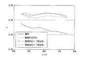
- FIG. 5 is a schematic cross-sectional view for explaining a model structure having an in-phase configuration with respect to the anti-phase configuration in FIG. 4. It is a cross-sectional schematic diagram for demonstrating the size of the model structure which performed the computer simulation of FIG. It is a figure which shows the result of the computer simulation of the light extraction efficiency of the organic EL element of the 3rd Embodiment of this invention, (a) is a thing with a period of 500 nm, (b) is a thing with a period of 1000 nm. . It is a cross-sectional schematic diagram for demonstrating the size of the model structure which performed the computer simulation of FIG.
- the first electrode is an anode and the second electrode is a cathode
- Either the top emission type or the bottom emission type may be applied to the organic EL element of the present invention.
- a bottom emission type configuration will be described as an example.
- the organic EL device of the present invention may include a layer not described below as long as the effects of the present invention are not impaired.
- FIG. 1 is a schematic cross-sectional view for explaining an example of the organic EL element according to the first embodiment of the present invention.
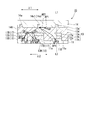
- An organic EL element 10 according to the first embodiment of the present invention includes an anode (first electrode) 12, an organic layer 13 including a light emitting layer made of an organic EL material, and a cathode (second electrode) on a substrate 11. 14 in order.
- the cathode 14 has a plurality of radiation starting point portions 14a periodically disposed on the surface 14A on the organic layer side.
- a dielectric layer 17 having a refractive index lower than that of the organic layer 13 and having a plurality of openings 17A (see FIG.
- the organic layer 13 has an opening inner side surface covering portion 13a that covers the inner surface 7a of the opening portion 17A.
- the period ⁇ 1 in which the opening 17A is arranged and the period ⁇ 2 in which the radiation starting point part 14a is arranged coincide at least in one direction in the element plane.
- the anode 12 includes an anode opening (first electrode opening) 12A (see FIG. 8G) that communicates with the opening 17A, and the substrate 11 communicates with the anode opening 12A.
- a recess 11A (see FIG. 8H) is provided.
- the organic layer 13 is further provided with a portion corresponding to the shape of the radiation starting point portion 14a (in the example of FIG. 1, a convex portion 13e) and an anode opening inner side surface covering portion (first electrode) covering the inner side surface 12a of the anode opening portion 12A. (Opening inner side surface covering portion) 13b and concave inner side surface covering portion 13c covering inner surface 11a of concave portion 11A.
- the portion 13e corresponding to the shape of the radiation starting point portion 14a is convex if the radiation starting point portion 14a is concave as shown in FIG. 1, and if the radiation starting point portion 14a is convex, , Become concave.
- FIG. 1 The configuration shown in FIG.
- the organic layer 13 is that of a bottom emission type organic EL element.
- the substrate 11 is disposed on the opposite side of the cathode 14 from the organic layer 13.
- the organic layer 13 further includes a dielectric layer 17 and a layered portion 13 d disposed between the opening inner side surface covering portion 13 a and the cathode 14.
- the organic layer 13 may be configured to include all the portions indicated by reference numerals 13a to 13e, or may be configured to include the portions indicated by reference numerals 13a to 13c and 13e without the layered portion 13d.
- the opening inner side surface covering part 13a, the anode opening inner side surface covering part 13b, and the concave inner side surface covering part 13c may be constituted by a part of the layers constituting the organic layer.
- the refractive index of the organic layer refers to the average refractive index of all the layers including the light emitting layer made of the organic EL material. . The same applies to other embodiments described later.
- the shape of the opening 17A, the anode opening 12A, and the recess 11A is not particularly limited as long as it has an effect of refracting light toward the substrate on the inner surface thereof. From the viewpoint of refracting the guided mode light closer to the vertical direction with respect to the anode surface, a shape in which the area on the opening on the cathode 14 side is smaller than the opening bottom area on the substrate 11 side is preferable. From the viewpoint of taking out the light straight to the substrate without refracting the light beam, a shape in which the opening bottom area on the substrate 11 side is smaller than the area on the opening on the cathode 14 side is preferable.
- the area of both bottom surfaces of the opening is smaller.
- the inner surfaces of the opening 17A, the anode opening 12A, and the recess 11A are arranged orthogonal to the anode surface and the substrate surface, but the present invention is not limited to such a configuration.
- the angle between these inner surfaces and the substrate surface is preferably 45 ° or more, more preferably 60 ° or more, and even more preferably 75 ° or more.
- This organic EL element 10 is a bottom emission type organic EL element that extracts light emitted from the light emitting layer from the substrate side. Therefore, the substrate 11 is a light-transmitting substrate and usually needs to be transparent to visible light.
- transparent to visible light means that it is only necessary to transmit visible light having a wavelength emitted from the light emitting layer, and does not need to be transparent over the entire visible light region.
- a smooth substrate having a transmittance in visible light of 400 to 700 nm of 50% or more is preferable.
- the material of the substrate 11 include a glass plate and a polymer plate.
- the glass plate include soda lime glass, barium / strontium-containing glass, lead glass, aluminosilicate glass, borosilicate glass, barium borosilicate glass, and quartz.
- the polymer plate include polycarbonate, polymethyl methacrylate, polyethylene terephthalate, polyethylene naphthalate, polyether sulfide, and polysulfone.
- the transmittance is preferably 50% or more and more preferably 70% or more with respect to the wavelength at which light emission has the maximum intensity.
- an opaque material can be used in addition to the same material as described above.
- a metal material such as stainless steel, Si, SiC, AlN, GaN, Nonmetallic materials such as GaAs and sapphire, and other substrate materials usually used in top emission type organic EL elements can be used.
- a material having high thermal conductivity is preferably used for the substrate.
- the thickness of the substrate 11 depends on the required mechanical strength and is not limited. The thickness is preferably 0.01 mm to 10 mm, more preferably 0.05 mm to 2 mm. However, in this embodiment, since the substrate 11 includes a plurality of recesses 11A, it is preferable that the substrate 11 be a material that can be processed more accurately. Although it does not limit as a preferable material, For example, quartz is mentioned.
- Each of the plurality of recesses 11A communicates with the opening 17A of the dielectric layer 17 through the anode opening 12A, and therefore has the same arrangement as the opening 17A.
- the concave portion 11A may be a dot-shaped concave portion (recesses that are discretely arranged), a line-shaped (parallel stripe shape) concave portion, or a combination of these in a plane.
- the arrangement of the recesses 11A in the element plane direction may be a one-dimensional arrangement or a two-dimensional arrangement in accordance with the periodic arrangement of the radiation starting point portions 14a.
- the anode 12 includes a plurality of anode openings 12A (see FIG. 8G).
- the inner surface 12a of the anode opening 12A is covered with the organic layer 13 (anode opening inner surface covering portion 13b).
- the upper surface of the anode 12 is covered with a dielectric layer 17.
- the anode opening 12A may be filled or may be partially filled.
- Each of the plurality of anode openings 12A communicates with the opening 17A, and thus has the same arrangement as the opening 17A.
- the anode opening 12A may be any of dot-like openings (openings arranged in a discrete manner), line-like openings, and a combination of these in-plane.
- the arrangement of the anode openings 12A in the element plane direction may be a one-dimensional arrangement or a two-dimensional arrangement in accordance with the periodic arrangement of the radiation starting point portions 14a.
- the anode 12 is an electrode for applying a voltage between the anode 14 and injecting holes from the anode 12 into the light emitting layer. It is preferable to use a material made of a metal, an alloy, a conductive compound, or a mixture thereof having a high work function. It is preferable to use a material having a work function of 4 eV or more and 6 eV or less so that the difference from the HOMO (Highest Occupied Molecular Orbital) level of the organic layer 13 in contact with the anode 12 does not become excessive.
- the material of the anode 12 is not particularly limited as long as it is a translucent and conductive material.
- conductive high conductivity doped with transparent inorganic oxides such as indium tin oxide (ITO), indium zinc oxide (IZO), tin oxide, zinc oxide, conductive polymers such as PEDOT: PSS, polyaniline, and arbitrary acceptors.
- transparent inorganic oxides such as indium tin oxide (ITO), indium zinc oxide (IZO), tin oxide, zinc oxide, conductive polymers such as PEDOT: PSS, polyaniline, and arbitrary acceptors.
- transparent carbon materials such as molecules, carbon nanotubes, and graphene.
- the anode 2 can be formed on the substrate 1 by, for example, sputtering, vacuum vapor deposition (resistance heating vapor deposition or electron beam vapor deposition), CVD, ion plating, coating, or the like.
- the thickness of the anode 12 is not limited, but is, for example, 10 to 2000 nm, preferably 50 to 1000 nm. If the thickness of the anode 12 is less than 10 nm, it is difficult to increase the volume of the dielectric layer 17 and scattering of the waveguide mode light is difficult. If the thickness of the anode 12 is larger than 2000 nm, the flatness of the organic layer 13 cannot be maintained and the transmittance of the anode is lowered.
- the dielectric layer 17 has a refractive index lower than that of the organic layer 13 and includes a plurality of openings 17A.
- the inner side surface 17a of the opening 17A is covered with the organic layer 13 (opening inner side surface covering portion 13a). As long as the inner surface 17a of the opening covers the inner surface 17a, the opening 17A may be filled or may be partially filled.
- Each of the plurality of openings 17A communicates with the recess 11A via the anode opening 12A. That is, the opening 17A may be a dot-like opening (opening arranged discretely), a line-like (parallel stripe-shaped) opening, or a combination of these in an in-plane manner.
- the arrangement in the element plane direction of the openings 17A may be a one-dimensional arrangement or a two-dimensional arrangement in accordance with the periodic arrangement of the radiation starting point portions.
- the material of the dielectric layer 17 is not particularly limited as long as it is a light-transmitting material and has a refractive index lower than that of the organic layer 13.
- metal fluorides such as SOG (typical refractive index: 1.25), MgF 2 (typical refractive index: 1.38), organic fluorine compounds such as PTFE, SiO 2 (typical refractive index: 1.45), various low-melting-point glasses, and porous materials.
- the thickness of the dielectric layer 17 is not limited, but is, for example, 10 to 2000 nm, and preferably 50 to 1000 nm.
- the thickness of the dielectric layer 17 is less than 10 nm, the organic layer must also be formed thin, and thus a punch-through current is likely to be generated and the internal quantum efficiency is lowered.
- the thickness of the dielectric layer 17 is greater than 2000 nm, it becomes difficult to maintain the flatness of the organic layer 13.
- the cathode 14 has a plurality of radiation starting points 14a periodically disposed on the surface 14A on the organic layer side.
- the radiation starting point portion 14a is arranged at a position overlapping with a portion other than the opening portion 17A of the dielectric layer 17 (substantial portion of the dielectric layer 17) 17B in plan view. It is not limited to this positional relationship.
- the radiation starting point portion 14a further includes a portion other than the anode opening 12A of the anode 12 (substantial portion of the anode 12) 12B and a portion other than the recess 11A of the substrate 11 (on the substrate 11). (Substantial part) It is arranged at a position overlapping 11B, but is not particularly limited to this positional relationship.
- the cathode 14 is an electrode for injecting electrons into the light emitting layer, and it is preferable to use a material made of a metal, an alloy, a conductive compound, or a mixture thereof having a small work function. It is preferable to use a material having a work function of 1.9 eV or more and 5 eV or less so that the difference from the LUMO (Lowest Unoccupied Molecular Orbital) level of the organic layer 13 in contact with the cathode 14 does not become excessive.
- Specific examples include materials such as Al, MgAg alloys, and alloys of Al and alkali (earth) metals such as AlLi and AlCa.
- the thickness of the cathode 14 is not limited, but is, for example, 30 nm to 1 ⁇ m, and preferably 50 to 500 nm. If the thickness of the cathode 14 is less than 30 nm, the sheet resistance increases and the driving voltage rises. When the thickness of the cathode 14 is greater than 1 ⁇ m, damage due to heat and radiation during film formation and mechanical damage due to film stress accumulate in the electrode and the organic layer.
- the shape is not limited to the concave shape, and may be a convex shape, an uneven shape, or the like.
- Each shape of the radiation starting point portion 14a when seen in a plan view may be a shape such as a dot-shaped unevenness (unevenly arranged discretely), a line-shaped (parallel stripe-shaped) unevenness, or the like.
- One radiation starting point portion 14a (unit structure of the radiation starting point portion) may be composed of one concave or convex structure, or may be composed of a concavo-convex structure forming a plurality of undulations.
- one radiation starting point portion 14a is preferably smaller than the size of a portion other than the opening 17A of the dielectric layer 17 (substantial portion of the dielectric layer 17) in plan view.
- the periodic array in the in-plane direction of the plurality of radiation starting point portions 14a may be a one-dimensional array or a two-dimensional array.
- the period in which the plurality of radiation starting point portions 14a are arranged is preferably 10 ⁇ m or less in which the SPP mode light can propagate. With such a period, before the SPP mode light is dissipated as heat, the SPP mode light can be scattered by the radiation starting point portion 14a and re-radiated as propagating light.
- the period of the arrangement of the radiation starting point portions 14a is the same as the period of the arrangement of the openings 17A in the dielectric layer 17 at least in one direction in the plane.
- the same period in one direction in the plane means that one of the real lattice vectors corresponding to the periodic structure of the radiation starting point portion 14a and one of the real lattice vectors corresponding to the periodic structure of the opening 17A coincide with each other.
- FIG. 2A is an example of the in-plane arrangement in the case where the radiation starting point portion 14a and the opening portion 17A are both in the form of dots. What is indicated by a solid line arrow in each figure is a real lattice vector common to the radiation starting point portion 14a and the opening portion 17A. In the case of this configuration, it is preferable that the radiation starting point portion 14a and the opening portion 17A coincide with each other with respect to another real lattice vector (dotted arrow) as shown in the left diagram of FIG.
- FIG. 2B is an example of the in-plane arrangement in the case where the radiation starting point portion 14a has a dot shape and the opening portion 17A has a line shape.
- FIG. 2C shows an example of in-plane arrangement in the case where the radiation starting point portion 14a is in a line shape and the opening portion 17A is in a dot shape.
- a solid line arrow in each figure is a real lattice vector common to the radiation starting point portion 14a and the opening portion 17A.
- the center of the opening portion 17A is located on the center line of the radiation starting point portion 14a or just between the adjacent opening portions 17A as shown in the three figures on the left side of FIG.
- FIG. 2D shows an example of the in-plane arrangement in the case where the radiation starting point portion 14a and the opening portion 17A are both linear. What is indicated by a solid arrow in each figure is a real lattice vector common to the radiation starting point portion 14A and the opening portion 17A.
- the center line of the radiation starting point portion 14a is preferably located on the center line of the opening portion 17A or just between the adjacent 17A.
- the organic layer 13 includes an opening inner surface covering portion 13a that covers the inner surface 17a of the opening 17A, an anode opening inner surface covering portion 13b that covers the inner surface 12a of the anode opening 12A, and an inner surface 11a of the recess 11A. It has a concave inner side surface covering portion 13c to be covered and a portion 13e corresponding to the shape of the radiation starting point portion 14a.
- the dielectric layer 17 and the layered portion 13 d disposed between the opening inner side surface covering portion 13 a and the cathode 14 are further provided.
- any material known as a material for an organic EL element can be used as a material for an organic EL element.
- the organic layer 13 may include a hole injection layer, a hole transport layer, an electron injection layer, an electron transport layer, and the like in addition to a light emitting layer made of an organic EL material.
- the hole injection layer is a layer that assists hole injection from the anode 12 to the light emitting layer 13.
- Such a hole injection layer is preferably a material that injects holes into the light emitting layer with lower electric field strength.
- the material for forming the hole injection layer is not particularly limited as long as it has the above function, and any material can be selected and used from known materials.
- the hole transport layer is a layer that transports holes to the light emitting region, and has a high hole mobility and a small ionization energy of usually 5.5 eV or less.
- the material for forming the hole transport layer is not particularly limited as long as it has the above-described function, and any material can be selected and used from known materials.
- the electron injection layer is a layer that assists electron injection from the cathode 14 to the organic layer 13.
- a material that injects electrons into the organic layer 13 with lower electric field strength is preferable.
- the material for forming the electron injection layer is not particularly limited as long as it has the above function, and any material can be selected and used from known materials.
- the electron transport layer is a layer that transports electrons to the light emitting region and has a high electron mobility.
- the material for forming the electron transport layer is not particularly limited as long as it has the above functions, and any material can be selected and used from known materials.
- the organic layer 13 may be formed by a dry process such as an evaporation method or a transfer method, or may be formed by a wet process such as a spin coating method, a spray coating method, a die coating method, or a gravure printing method.
- the thickness of the organic layer 13 is not limited, but is, for example, 50 to 2000 nm, and preferably 100 to 1000 nm. If the thickness of the organic layer 13 is less than 50 nm, quenching other than SPP coupling by the cathode 14 occurs, such as a decrease in internal quantum efficiency due to a punch-through current or lossy surface wave mode coupling. When the thickness of the organic layer 13 is greater than 2000 nm, the drive voltage increases.
- a part (AP1) of the light emitted from the AP point of the light emitting layer included in the organic layer 13 is captured as SPP mode light on the surface 14A of the cathode 14 through the near field around the light emitting point. It is well known that such energy transfer to SPP mode light occurs when a light emitting molecule and a metal layer are close to each other in a general organic EL element having a cathode made of a metal layer.
- the SPP mode light moves along the surface 14A (arrow AP2) and is emitted from the radiation starting point portion 14a 1 (14a) to become propagating light.
- the light passes through the dielectric layer 17 and the like and enters the substrate 11 (arrows BP1, BP2, BP3, BP4) and is taken out of the substrate.
- the substrate 11 arrows BP1, BP2, BP3, BP4
- the arrow AP1 schematically shows the propagation of a part of the light in order to explain the function and effect of the present invention.
- the light indicated by the arrow AP2 and the arrows BP1 to BP4 and the light indicated by the arrows CP1 to CP4 to be described later are also schematically shown.
- the light BP1 is light that travels perpendicularly to the substrate 11 toward the substrate. This light is not refracted at the interface between the organic layer 13 and the dielectric layer 17, the interface between the dielectric layer 17 and the anode 12, and the interface between the anode 12 and the substrate 11. Then, the substrate 11 is taken out and taken out to the outside.
- the light BP2 re-radiated from the radiation starting point portion 14a 1 (14a) is refracted at the interface between the organic layer 13a (13) and the dielectric layer 17 (the inner side surface 17a of the opening 17A) and passes through the dielectric layer 17.
- the light is totally reflected when it enters the interface between the anode 12 and the substrate 11 (for example, glass) or the interface between the substrate 11 and air at an angle greater than the critical angle, but the light is reflected by refraction at the inner surface 17a of the opening 17A.
- the direction of travel changes toward the normal line of the substrate 11. Therefore, the light that can avoid total reflection at the interface between the anode 12 and the substrate 11 and the interface between the substrate 11 and air is increased, and the light extraction efficiency is improved. That is, the light extraction efficiency is improved by having the configuration including the inner surface 17a of the opening 17A.
- the light traveling direction of the light BP3 also changes closer to the normal line of the substrate 11 due to refraction at the interface between the organic layer 13a (13) and the dielectric layer 17 (the inner surface 17a of the opening 17A). Therefore, similarly to the light BP2, the light that can avoid total reflection at the interface between the anode 12 and the substrate 11 and the interface between the substrate 11 and the air is increased, and the light extraction efficiency is improved. Further, even when the light BP4 is refracted at the interface between the organic layer 13c (13) and the convex portion 11B of the substrate 11 (the inner surface 11a of the concave portion 11A), the light traveling direction is normal to the substrate 11 due to this refraction. It changes to the side. Therefore, similarly, the light that can avoid total reflection at the interface between the anode 12 and the substrate 11 and the interface between the substrate 11 and air is increased, and the effect of improving the light extraction efficiency can be obtained.
- the vicinity of the shortest distance between the cathode 14 and the anode 12 has the highest current density and the amount of light emission increases.
- the light emission at the CPl and CPr points of the light emitting layer included in the organic layer 13 schematically shows the light emission at the point where this light emission amount is large.
- the light CP 1 is light that travels to the substrate side in the direction perpendicular to the substrate 11 and is refracted at the interface between the organic layer 13 and the substrate 11. Without going through the substrate 11, it is taken out.
- the light CP2 is refracted at the interface between the organic layer 13a (13) and the dielectric layer 17B (17) (the inner surface 17a of the opening 17A), passes through the dielectric layer 17B (17), and passes through the dielectric layer 17B ( 17) and refracted at the interface between the anode 12 and the anode 12, and after being refracted at the interface between the anode 12 and the substrate 11, it can be taken out through the substrate 11.
- the light CP2 travels from the organic layer 13 to the dielectric layer 17, the refraction at the interface between the organic layer 13a (13) and the dielectric layer 17B (17) (the inner surface 17a of the opening 17A)
- the direction of travel changes toward the normal line of the substrate 11.
- the light When light is incident at an angle greater than the critical angle at the interface between the anode 12 and the substrate 11 (for example, glass) or the interface between the substrate 11 and air, the light is totally reflected, but is refracted at the inner surface 17a of the opening 17A. As a result, the traveling direction of the light changes toward the normal line of the substrate 11. Therefore, the light that can avoid total reflection at the interface between the anode 12 and the substrate 11 and the interface between the substrate 11 and air is increased, and the light extraction efficiency is improved. The same effect can be obtained for the light CP3.
- the light CP4 traveling through the organic layer 13 from the CP1 point is refracted at the interface between the organic layer 13c and the convex portion 11B of the substrate 11 (inner side surface 11a of the concave portion 11A), the direction of travel of light due to this refraction. Changes toward the normal of the substrate 11. Therefore, similarly, the light that can avoid total reflection at the interface between the anode 12 and the substrate 11 and the interface between the substrate 11 and air is increased, and the effect of improving the light extraction efficiency can be obtained. With respect to light emitted at the CPr point of the light emitting layer included in the organic layer 13, the same effect as the light emitted at the CPl point can be obtained.
- the SPP mode light propagates at the radiation starting point on the cathode surface. It can be re-radiated as light and extracted. Further, the propagating light extracted from the cathode surface is applied to the substrate at the interface between the organic layer and the dielectric layer (the inner surface of the opening) and the interface between the organic layer and the convex portion of the substrate (the inner surface of the recess). The amount of light extracted from the substrate to the outside can be increased by refracting toward the linear direction.
- FIG. 3 shows an organic EL having a configuration in which the relative position between the portion 17B other than the opening 17A of the dielectric layer 17 and the radiation starting point portion 14a of the cathode 14 is shifted by a half cycle.
- FIG. 3 shows an element.
- the radiation starting point portion 14a of the cathode 14 is positioned so as to overlap with a portion (substantial portion of the dielectric layer) 17B other than the opening portion 17A of the dielectric layer 17 in plan view. Has been placed.
- FIG. 1 shows an organic EL having a configuration in which the relative position between the portion 17B other than the opening 17A of the dielectric layer 17 and the radiation starting point portion 14a of the cathode 14 is shifted by a half cycle.
- the central axis L1 perpendicular to the substrate 11 of the radiation starting point portion 14a of the cathode 14 in the cross section perpendicular to the substrate surface is the portion 17B of the dielectric layer 17 other than the opening portion 17A. It coincides with the central axis L2.
- the relative positional relationship between the radiation starting point of the cathode and the portion other than the opening of the dielectric layer (substantial portion of the dielectric layer 17) is as shown in FIG. 1, that is, the radiation starting point portion of the cathode 14.
- a configuration in which 14a has a relative positional relationship overlapping with a substantial part of the dielectric layer in plan view may be referred to as “reverse phase”.
- the radiation starting point portion 14a of the cathode 14 is formed in a portion (substantial portion of the dielectric layer) 17B other than the opening portion 17A of the dielectric layer 17 in plan view. It is arranged in a position that does not overlap.
- the central axis L1 perpendicular to the substrate of the radiation starting point portion 14a of the cathode 14 in the cross section perpendicular to the substrate surface is the central axis L2 of the portion 17B of the dielectric layer 17 other than the opening 17A. The configuration is shifted by half a cycle.
- the relative positional relationship between the radiation starting point portion 14a of the cathode 14 and a portion (substantial portion of the dielectric layer 17) 17B of the dielectric layer 17 other than the opening portion 17A is as shown in FIG.
- a configuration in which the radiation starting point portion 14a of the cathode 14 has a relative positional relationship that does not overlap the substantial portion 17B of the dielectric layer 17 in plan view may be referred to as “in phase”.
- the organic EL device of the present invention may have either “in-phase” or “reverse phase” configuration. As will be described later, approximately the same light extraction efficiency can be obtained between “in phase” and “reverse phase”.
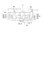
- FIG. 4 is a schematic cross-sectional view for explaining an example of the organic EL element according to the second embodiment of the present invention.
- An organic EL element 20 according to the second embodiment of the present invention includes, on a substrate 21, an anode 22, an organic layer 23 including a light emitting layer made of an organic EL material, and a cathode 24 in this order.
- the cathode 24 has a plurality of radiation starting points 24a periodically arranged on the surface 24A on the organic layer side.
- a dielectric layer 27 having a refractive index lower than that of the organic layer 23 and having a plurality of openings 27A (see FIG. 9A) is provided.
- the organic layer 23 has an opening inner side surface covering portion 23a that covers the inner side surface 27a of the opening 27A, and a period ⁇ 1 in which the opening 27A is disposed and a period ⁇ 2 in which the radiation starting point portion 24a is disposed are at least elements. Match in one direction in the plane.
- the organic EL element according to the second embodiment is exemplified by a case where the emission starting point of the cathode has a “reverse phase” configuration having a relative positional relationship overlapping with a substantial part of the dielectric layer in plan view. I will explain.
- the organic layer 23 further includes a portion (in the example of FIG. 4, a convex portion 23c) corresponding to the shape of the radiation starting point portion 24a.
- the organic layer 23 further includes a dielectric layer 27 and a layered portion 23 b disposed between the opening inner side surface covering portion 23 a and the cathode 24.
- the organic layer 23 may be configured to include all the portions indicated by reference numerals 23a to 23c, or may include the portions indicated by reference numerals 23a and 23c without the layered portion 23b.
- the portion of the organic layer 23 corresponding to the shape of the radiation starting point 24a becomes a convex portion 23c if the radiation starting point 24a is concave as shown in FIG. 4, and if the radiation starting point 24a is convex. It becomes a recess.
- the opening inner side surface covering portion 23 a may be constituted by a part of the layers constituting the organic layer 23.
- the shape of the opening 27A is not particularly limited as long as it has an effect of refracting light toward the substrate on its inner surface. From the viewpoint of refracting the guided mode light closer to the vertical direction with respect to the anode surface, a shape in which the area on the opening on the cathode 24 side is smaller than the area on the bottom of the opening on the substrate 21 side is preferable. From the viewpoint of taking out the light straight to the substrate without refracting the light beam, a shape in which the opening bottom area on the substrate 21 side is smaller than the area on the opening on the cathode 24 side is preferable. From the viewpoint of refracting guided mode light and extracting it with a smaller propagation distance, the smaller the area of both bottom surfaces of the opening, the better.
- the inner side surface of the opening is configured to be orthogonal to the substrate surface, but is not limited to this configuration.
- the angle of the inner surface with respect to the substrate surface is preferably 45 ° or more, more preferably 60 ° or more, and even more preferably 75 ° or more.
- the organic EL element 20 is a bottom emission type organic EL element, like the organic EL element 10 of the first embodiment, but may be a top emission type.
- the material and thickness of the substrate 21 the same materials as those of the substrate 11 can be used.
- the same materials as those in the first embodiment can be used.
- the dielectric layer 27 has a refractive index lower than that of the organic layer 23 and includes a plurality of openings 27A.
- the inner surface 27a of the opening 27A is covered with the organic layer 23 (opening inner surface covering portion 23a). As long as the inner surface 27a of the opening covers the inner surface 27a, the opening 27A may be filled or may be partially filled.
- the same materials as those in the first embodiment can be used. Further, the shape and arrangement of the openings 27A can be the same as those in the first embodiment.
- the organic layer 23 includes an opening inner surface covering portion 23a that covers the inner surface 27a of the opening 27A, a dielectric layer 27, a layered portion 23b disposed between the opening inner surface covering portion 23a, and the cathode 24, and radiation. And a convex portion 23c corresponding to the shape of the starting portion 24a.
- the material of the light emitting layer any material known as a material for an organic EL element can be used as in the first embodiment.
- the thickness of the organic layer 23 is the same as that in the first embodiment. Similar to the first embodiment, the organic layer 23 may include a hole injection layer, a hole transport layer, an electron injection layer, an electron transport layer, and the like in addition to a light emitting layer made of an organic EL material.
- the same materials as those in the first embodiment can be used.
- the shape and arrangement of the radiation starting point 24a can be the same as those of the radiation starting point of the first embodiment.
- a part (AQ1) of the light emitted from the AQ point of the light emitting layer included in the organic layer 23 is captured as SPP mode light on the surface 24A of the cathode 24 via the near field around the light emitting point.
- the SPP mode light moves along the surface 24A (arrow AQ2), is re-radiated at the radiation starting point 24a 1 (24a) to become propagating light, and further passes through the dielectric layer 27 and the like and enters the substrate 21. , Taken out of the substrate.
- the light emitted at the AQ point of the organic layer 23 travels in all directions, there is naturally light traveling in a direction other than the arrow AQ1.
- An arrow AQ1 schematically shows the propagation of a part of the light in order to explain the function and effect of the present invention.
- the light shown by the arrows AQ2 and BQ1 to BQ3 and the light shown by the arrows CQ1 to CQ3 described later are also schematically shown.
- the light BQ1 is light that travels perpendicularly to the substrate 21 toward the substrate side, and the organic layer 23b (23) Without being refracted at the interface between the dielectric layer 27 and the dielectric layer 27, the interface between the dielectric layer 27 and the anode 22, and the interface between the anode 22 and the substrate 21, and proceeds through the dielectric layer 27, the anode 22 and the substrate 21, Take out to the outside.
- the light BQ2 radiated from the radiation starting point 24a 1 (24a) is refracted at the interface between the organic layer 23a (23) and the dielectric layer 27B (27) (the inner side surface 27a of the opening 27A), and the dielectric layer 27B. (27) is transmitted, refracted at the interface between the dielectric layer 27B (27) and the anode 22, travels through the anode 22, refracts at the interface between the anode 22 and the substrate 21, and then passes through the substrate 21 to the outside. Can be taken out.
- the light BQ2 travels from the organic layer 23a (23) to the dielectric layer 27, due to refraction at the interface between the organic layer 23a (23) and the dielectric layer 27B (27) (inner side surface 27a of the opening 27A).
- the angle of incidence on the anode 22 and the substrate 21 changes to a small angle (an angle closer to the normal direction of the substrate 21).
- the substrate 21 for example, glass
- the critical angle the light is totally reflected.
- the refraction at the inner surface 27a of the opening 27A causes the traveling direction of the light to be the substrate. It changes toward 21 normals.
- the light extraction efficiency is improved by having the configuration including the inner side surface 27a of the opening 27A.
- the light BQ3 also changes its traveling direction toward the normal line of the substrate 21 due to refraction at the interface between the organic layer 23a (23) and the dielectric layer 27B (27) (the inner surface 27a of the opening 27A). Therefore, as in the case of the light BQ2, there is an increase in light that can avoid total reflection at the interface between the anode 22 and the substrate 21 and at the interface between the substrate 21 and air, thereby improving the light extraction efficiency.
- the light CQ1 is light that travels to the substrate side in a direction perpendicular to the substrate, and is not refracted at the interface between the organic layer 23 and the substrate 21. It proceeds through the substrate 21 and is taken out to the outside.
- the light CQ2 is refracted at the interface between the organic layer 23a (23) and the dielectric layer 27 (the inner surface 27a of the opening 27A), passes through the dielectric layer 27, and is transmitted at the interface between the dielectric layer 27 and the anode 22. After being refracted and traveling through the anode 22 and refracting at the interface between the anode 22 and the substrate 21, it can be taken out through the substrate 21.
- the light traveling direction is changed due to refraction at the interface between the organic layer 23a (23) and the dielectric layer 27 (the inner side surface 27a of the opening 27A). It changes closer to the normal line of the substrate 21.
- the critical angle at the interface between the anode 22 and the substrate 21 for example, glass
- the light is totally reflected, but refraction at the inner surface 27a of the opening 27A.
- the traveling direction of the light changes toward the normal line of the substrate 21. Therefore, light that can avoid total reflection at the interface between the anode 22 and the substrate 21 and at the interface between the substrate 21 and air is increased, and the light extraction efficiency is improved. The same effect can be obtained for the light CQ3.
- the SPP mode light propagates at the radiation starting point on the cathode surface. It can be re-radiated and extracted as light, and the propagating light extracted from the cathode surface is refracted toward the normal direction of the substrate at the interface between the organic layer and the dielectric layer (the inner surface of the opening). The amount of light extracted from the substrate to the outside can be increased.
- FIG. 5 is a schematic cross-sectional view for explaining an example of the organic EL element according to the third embodiment of the present invention.
- An organic EL device 30 according to the third embodiment of the present invention includes, on a substrate 31, an anode 32, an organic layer 33 including a light emitting layer made of an organic EL material, and a cathode 34 in this order.
- the cathode 34 has a plurality of radiation starting point portions 34a periodically arranged on the surface 34A on the organic layer side.
- a dielectric layer 37 having a refractive index lower than that of the organic layer 33 and having a plurality of openings 37A (see FIG.
- the organic layer 33 has an opening inner side surface covering portion 33a that covers the inner surface 37a of the opening portion 37A, and a period ⁇ 1 in which the opening portion 37A is disposed and a period ⁇ 2 in which the radiation starting point portion 34a is disposed are at least elements. Match in one direction in the plane.
- the anode 32 includes an anode opening 32A (see FIG. 10A) communicating with the opening 37A.
- the organic EL device according to the third embodiment will be described by taking as an example a “reverse phase” configuration in which the emission starting point of the cathode has a relative positional relationship with the substantial part of the dielectric layer in plan view. .
- the organic layer 33 further includes a portion corresponding to the shape of the radiation starting point portion 34a (a convex portion 33d in the example of FIG. 5) and an anode opening inner side surface covering portion 33b that covers the inner side surface 32a of the anode opening portion 32A. Is.
- the organic layer 33 further includes a dielectric layer 37 and a layered portion 33 c disposed between the opening inner side surface covering portion 33 a and the cathode 34.
- the organic layer 33 may be configured to include all the portions indicated by reference numerals 33a to 33d, or may include the portions indicated by reference numerals 33a, 33b, and 13d without the layered portion 33c.
- the portion 33d corresponding to the shape of the radiation starting point 34a is convex if the radiation starting point 34a is concave as shown in FIG. 5, and if the radiation starting point 34a is convex. , Become concave.
- the opening inner side surface covering portion and the anode opening inner side surface covering portion may be constituted by a part of the layers constituting the organic layer.
- the shapes of the opening 37A and the anode opening 32A are not particularly limited as long as they have an effect of refracting light toward the substrate on the inner side surfaces thereof.
- a shape in which the area on the opening on the cathode 34 side is smaller than the bottom area of the opening on the substrate 31 side is preferable.
- a shape in which the bottom area of the opening on the substrate 31 side is smaller than the area on the opening on the cathode 34 side is preferable.
- the inner surfaces of the opening and the anode opening are arranged so as to be orthogonal to the substrate surface.
- the angle between these inner surfaces and the substrate surface is preferably 45 ° or more, more preferably 60 ° or more, and even more preferably 75 ° or more.
- the organic EL element 30 is a bottom emission type organic EL element, like the organic EL element of the first embodiment, but may be a top emission type.
- the material and thickness of the substrate 31 the same materials as those of the substrate 11 can be used.
- the anode 32 includes a plurality of anode openings 32 ⁇ / b> A, and an inner surface 32 a of the anode openings 32 ⁇ / b> A is covered with an organic layer 33.
- the anode opening 32A may be filled or may be partially filled.
- the material and thickness of the anode 32 the same materials as those in the first embodiment can be used.
- the shape and arrangement of the anode openings 32A can be the same as in the first embodiment.
- the dielectric layer 37 has a refractive index lower than that of the organic layer 33 and includes a plurality of openings 37A.
- the inner side surface 37a of the opening 37A is covered with an organic layer 33 (opening inner side surface covering portion 33a). As long as the inner surface 37a of the opening covers the inner surface 37a, the opening 37A may be filled or may be partially filled.
- the material and thickness of the dielectric layer 37 the same materials as those in the first embodiment can be used.
- the shape and arrangement of the openings 37A can be the same as in the first embodiment.
- the organic layer 33 corresponds to the shape of the opening inner surface covering portion 33a covering the inner surface 37a of the opening 37A, the anode opening inner surface covering portion 33b covering the inner surface of the anode opening 32A, and the radiation starting point portion 34a. 33d. Further, the example shown in FIG. 5 further includes a dielectric layer 37 and a layered portion 33 c disposed between the opening inner side surface covering portion 33 a and the cathode 34.
- the material of the light emitting layer any material known as a material for an organic EL element can be used as in the first embodiment.
- the organic layer 33 may include a hole injection layer, a hole transport layer, an electron injection layer, an electron transport layer, and the like in addition to the light emitting layer made of an organic EL material, as in the first embodiment.
- the same materials as those in the first embodiment can be used.
- the shape and arrangement of the radiation starting point 34a can be the same as those of the radiation starting point of the first embodiment.
- a part (AR1) of the light emitted from the AR point of the light emitting layer included in the organic layer 33 is captured as SPP mode light on the surface 34A of the cathode 34 through the near field around the light emitting point.
- the SPP mode light moves along the surface 34A (arrow AR2), is re-radiated at the radiation starting point 34a 1 (34a) to become propagating light, and further passes through the dielectric layer 37 and the like and enters the substrate 31. , Taken out of the substrate.
- the arrow AR1 schematically shows the propagation of a part of the light in order to explain the function and effect of the present invention.
- the light indicated by the arrow AR2 and the arrows BR1 to BR3 and the light indicated by the arrows CR1 to CR3 to be described later are also schematically shown.
- the light BR1 is light that travels perpendicularly to the substrate 31 toward the substrate side.
- the light passes through the dielectric layer 37, the anode 32, and the substrate 31 without being refracted at the interface with the layer 37, the interface between the dielectric layer 37 and the anode 32, and the interface between the anode 32 and the substrate 31. It is.
- the light BR2 re-radiated at the radiation start point 34a 1 (34a) is refracted at the interface between the organic layer 33a (33) and the dielectric layer 37B (37) (the inner side surface 37a of the opening 37A), and the dielectric layer 37, refracts at the interface between the dielectric layer 37 ⁇ / b> B (37) and the anode 32, travels through the anode 32, refracts at the interface between the anode 32 and the substrate 31, and then takes out through the substrate 31 to the outside. Can be.
- the refraction at the interface between the organic layer 33a (33) and the dielectric layer 37B (37) causes refraction of the anode 32.
- the incident angle to the substrate 31 is changed to a small angle (an angle closer to the normal direction of the substrate 31).
- the light extraction efficiency is improved by having the configuration including the inner side surface 37a of the opening 37A.
- the light traveling direction changes closer to the normal line of the substrate 31 due to refraction at the interface between the organic layer 33a (33) and the dielectric layer 37B (37) (the inner surface 37a of the opening 37A). Therefore, as in the case of the light BR2, there is an increase in light that can avoid total reflection at the interface between the substrate and air, and the light extraction efficiency can be improved.
- the current density is highest near the shortest distance between the cathode 34 and the anode 32, and the amount of light emission is increased.
- the light emission at the CRl and CRr points of the light emitting layer included in the organic layer 33 schematically shows the light emission at the point where the light emission amount is large.
- the light CR1 is light traveling toward the substrate side in a direction perpendicular to the substrate 31, and is refracted at the interface between the organic layer 33 and the substrate 31. Without going through the substrate 31, it is taken out.
- the light CR2 is refracted at the interface between the organic layer 33a (33) and the dielectric layer 37B (37) (the inner surface 37a of the opening 37A), passes through the dielectric layer 37B (37), and passes through the dielectric layer 37B ( 37) and refracted at the interface between the anode 32 and the anode 32, and after being refracted at the interface between the anode 32 and the substrate 31, it can be taken out through the substrate 31 to the outside.
- the light CR2 travels from the organic layer 33 to the dielectric layer 37, the refraction at the interface between the organic layer 33a (33) and the dielectric layer 37B (37) (the inner surface 37a of the opening 37A) causes the light to pass through.
- the direction of travel changes toward the normal line of the substrate 31.
- the light is incident at an angle greater than the critical angle at the interface between the anode 32 and the substrate 31 (for example, glass) or the interface between the substrate 31 and air, the light is totally reflected, but refraction at the inner surface 37a of the opening 37A.
- the traveling direction of the light changes toward the normal line of the substrate 31. Therefore, light that can avoid total reflection at the interface between the anode 32 and the substrate 31 and at the interface between the substrate 31 and air is increased, and the light extraction efficiency is improved.
- the same effect can be obtained for the light CR3. With respect to light emitted at the CRr point of the light emitting layer included in the organic layer 33, the same effect as the light emitted at the CRl point can be obtained.
- the organic EL device of the present invention even if light emitted from the light emitting layer included in the organic layer is captured as SPP mode light on the cathode surface, the SPP mode light is regenerated at the radiation starting point on the cathode surface.
- the light extracted from the cathode surface is refracted from the normal direction of the substrate at the interface between the organic layer and the dielectric layer (inner side surface of the opening), and is extracted from the substrate. The amount of light extracted to the can be increased.
- FIG. 6 is a diagram illustrating an example of an image display device including the organic EL element.
- the image display device 100 shown in FIG. 6 is a so-called passive matrix type image display device.
- the anode wiring 104, the anode auxiliary wiring 106, the cathode wiring 108, the insulating film 110, and the cathode partition 112 are used.
- a sealing plate 116 and a sealing material 118 are used.
- a plurality of anode wirings 104 are formed on the substrate 11 of the organic EL element 10.
- the anode wirings 104 are arranged in parallel at a constant interval.
- the anode wiring 104 is made of a transparent conductive film, and for example, ITO can be used.
- the thickness of the anode wiring 104 can be set to 100 nm to 150 nm, for example.
- An anode auxiliary wiring 106 is formed on the end of each anode wiring 104.
- the anode auxiliary wiring 106 is electrically connected to the anode wiring 104.
- the anode auxiliary wiring 106 functions as a terminal for connecting to the external wiring on the end side of the substrate 11, and is connected to an external driving circuit (not shown) via the anode auxiliary wiring 106.
- a current can be supplied to the anode wiring 104.
- the anode auxiliary wiring 106 is made of a metal film having a thickness of 500 nm to 600 nm, for example.
- a plurality of cathode wirings 108 are provided on the organic EL element 10.
- the plurality of cathode wirings 108 are arranged so as to be parallel to each other and orthogonal to the anode wiring 104.
- Al or an Al alloy can be used for the cathode wiring 108.
- the thickness of the cathode wiring 108 is, for example, 100 nm to 150 nm.
- a cathode auxiliary wiring (not shown) is provided at the end of the cathode wiring 108, similarly to the anode auxiliary wiring 106 for the anode wiring 104, and is electrically connected to the cathode wiring 108. Therefore, a current can flow between the cathode wiring 108 and the cathode auxiliary wiring.
- an insulating film 110 is formed on the substrate 11 so as to cover the anode wiring 104.
- a rectangular opening 120 is provided in the insulating film 110 so as to expose a part of the anode wiring 104.
- the plurality of openings 120 are arranged in a matrix on the anode wiring 104.
- the organic EL element 10 is provided between the anode wiring 104 and the cathode wiring 108. That is, each opening 120 becomes a pixel. Accordingly, a display area is formed corresponding to the opening 120.
- the film thickness of the insulating film 110 can be, for example, 200 nm to 100 nm, and the size of the opening 120 can be, for example, 100 ⁇ m ⁇ 100 ⁇ m.
- the organic EL element 10 is located between the anode wiring 104 and the cathode wiring 108 in the opening 120.
- the anode 12 of the organic EL element 10 is in contact with the anode wiring 104 and the cathode 14 is in contact with the cathode wiring 108.
- the thickness of the organic EL element 10 can be set to, for example, 150 nm to 200 nm.
- a plurality of cathode partition walls 112 are formed on the insulating film 110 along a direction perpendicular to the anode wiring 104.
- the cathode partition 112 plays a role for spatially separating the plurality of cathode wirings 108 so that the wirings of the cathode wirings 108 do not conduct with each other. Accordingly, the cathode wiring 108 is disposed between the adjacent cathode partition walls 112.
- the size of the cathode partition 112 for example, the one having a height of 2 ⁇ m to 3 ⁇ m and a width of 10 ⁇ m can be used.
- the substrate 11 is bonded to each other with a sealing plate 116 and a sealing material 118 interposed therebetween. Thereby, the space in which the organic EL element 10 is provided can be sealed, and the organic EL element 10 can be prevented from being deteriorated by moisture in the air.
- a sealing plate 116 for example, a glass substrate having a thickness of 0.7 mm to 1.1 mm can be used.
- a current can be supplied to the organic EL element 10 via the anode auxiliary wiring 106 and the cathode auxiliary wiring (not shown) by a driving device (not shown) to cause the light emitting layer to emit light. Then, light can be emitted from the substrate 11 through the substrate 11.
- An image can be displayed on the image display device 100 by controlling the light emission and non-light emission of the organic EL element 10 corresponding to the above-described pixel by the control device.
- FIG. 7 is a diagram illustrating an example of an illumination device including the organic EL element 10 described above.
- the illumination device 200 shown in FIG. 7 includes the organic EL element 10 described above, and a terminal 202 that is installed adjacent to the substrate 11 (see FIG. 1) of the organic EL element 10 and connected to the anode 12 (see FIG. 1).
- the terminal 203 is connected to the cathode 14 (see FIG. 1), and the lighting circuit 201 is connected to the terminal 202 and the terminal 203 to drive the organic EL element 10.
- the lighting circuit 201 has a DC power source (not shown) and a control circuit (not shown) inside, and supplies a current between the anode layer 12 and the cathode 14 of the organic EL element 10 through the terminal 202 and the terminal 203. Then, the organic EL element 10 is driven to emit light from the light emitting layer, and light is emitted through the substrate 11 to be used as illumination light.
- the light emitting layer may be made of a light emitting material that emits white light, and each of the organic EL elements 10 using light emitting materials that emit green light (G), blue light (B), and red light (R). A plurality of them may be provided so that the combined light is white.
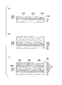
- the manufacturing method of the organic EL element according to the first embodiment of the present invention will be described with reference to FIG. First, as shown in FIG. 8A, the anode 12 and the dielectric layer 17 are formed in order on the substrate 11.
- the method for forming the anode 12 and the dielectric layer 17 is not particularly limited. For example, a resistance heating vapor deposition method, an electron beam vapor deposition method, a sputtering method, an ion plating method, a CVD method, or the like can be used.
- the surface treatment includes high-frequency plasma treatment, sputtering treatment, corona treatment, UV ozone irradiation treatment, ultraviolet irradiation treatment, oxygen plasma treatment, and the like.
- anode buffer layer (not shown) instead of or in addition to the surface treatment of the anode 12.
- anode buffer layer is applied by a wet process, spin coating, casting, micro gravure coating, gravure coating, bar coating, roll coating, wire bar coating, dip coating
- the film can be formed using a coating method such as a spray method, a spray coating method, a screen printing method, a flexographic printing method, an offset printing method, or an inkjet printing method.
- the anode opening 12A and the opening 17A communicating with each other are formed so as to penetrate the anode 12 and the dielectric layer 17 formed in the step of FIG.
- a method using photolithography can be used.
- a positive resist solution is applied on the dielectric layer 17, and the excess resist solution is removed by spin coating or the like to form a resist layer 19. To do.
- FIG. 8C the resist layer 19 is exposed with a predetermined pattern corresponding to the opening 17A (see FIG. 8F) (exposed portion 19a). Then, the resist layer 19a in the exposed pattern portion of the resist layer 19 is removed using a developer. As a result, the surface of the dielectric layer 17 is exposed corresponding to the exposed pattern portion (FIG. 8D).
- the dielectric layer 17 is etched away as shown in FIG.
- the etching either dry etching or wet etching can be used.
- the shape of the opening 17A can be controlled by combining isotropic etching and anisotropic etching.
- dry etching reactive ion etching (RIE) using dielectric coupling plasma or capacitive coupling plasma can be used.
- wet etching a solution of a metal salt such as an iron chloride aqueous solution or a method of immersing in an acid such as dilute hydrochloric acid or dilute sulfuric acid can be used. By this etching, the surface of the anode 12 is exposed corresponding to the pattern.
- RIE reactive ion etching
- wet etching a solution of a metal salt such as an iron chloride aqueous solution or a method of immersing in an acid such as dilute hydrochloric acid or dilute sulfuric acid can be used.
- FIG. 8F a resist removing solution or the like
- FIG. 8G the exposed portion of the anode 12 is removed using the dielectric layer 17 as a mask. Etch away.
- a method similar to the method described with reference to FIG. 8F can be used.
- the anode 12 is selectively selected without significantly affecting the dielectric layer 17 by changing the etching conditions. It can be etched. Thereby, the surface of the substrate 11 is exposed corresponding to the pattern, and the anode opening 12A is formed.
- FIG. 8F and FIG. 8G can be regarded as a process of forming the opening 17A and the anode opening 12A that penetrate through the anode 12 and the dielectric layer 17 and communicate with each other.
- the exposed portion of the substrate 11 is removed by etching using a portion other than the portion where the communicating opening 17A and the anode opening 12A are formed as a mask.
- etching a method similar to the method described with reference to FIGS. 8F and 8G can be used, but the dielectric layer 17 and the anode 12 are not significantly affected by changing the etching conditions.
- the substrate 11 can be selectively etched. Thereby, the concave portion 11A communicating with the opening 17A and the anode opening 12A can be formed corresponding to the pattern. Conversely, the portion other than the concave portion 11A becomes the convex portion 11B. According to this method, since it is not necessary to prepare a mask separately and perform photolithography, the concave portion 11A can be easily formed.
- the inner surface 17a of the opening 17A, the inner surface 12a of the anode opening 12A, and the inner surface 11a of the recess 11A are covered, and the dielectric layer 17 and the opening inner surface are covered.
- An organic layer 13 including a light emitting layer made of an organic EL material that covers the portion 13a is formed.
- the organic layer 13 includes an opening inner side surface covering portion 13a, an anode opening inner side surface covering portion 13b, a concave inner side surface covering portion 13c, and a layered portion 13d.
- a conventionally known method can be used to form the organic layer 13 and is not limited. For example, methods such as a vacuum deposition method, a spin coating method, a casting method, and an LB method can be used.
- a concavo-convex structure is formed on the surface of the organic layer 13 so as to have a convex portion 13e (see FIG. 1) at a position corresponding to the radiation starting point portion 14a of the cathode 14 to be formed later.
- a method using photolithography can be used for forming the unevenness. In order to do this, as shown in FIG. 8J, first, a positive resist solution is applied on the organic layer 13, and the excess resist solution is removed by spin coating or the like to form a resist layer 29. .
- the exposed portion of the organic layer 13 is removed by etching to form a convex portion 13e.
- etching either dry etching or wet etching can be used.
- the shape of the convex portion 13e can be controlled by combining isotropic etching and anisotropic etching.
- dry etching reactive ion etching (RIE), oxygen plasma ashing, or the like can be used.
- wet etching a method of immersing in dilute hydrochloric acid, dilute sulfuric acid, or various organic solvents can be used.
- a concavo-convex structure including a convex portion 13e corresponding to the radiation starting point portion 14a can be formed on the surface of the organic layer 13 corresponding to the pattern. Since photolithography has a positioning accuracy up to about 1 ⁇ m, it can be formed such that the radiation starting point of the cathode and the anode opening overlap in a plan view.
- a cathode material is vapor-deposited on the organic layer 13, and the cathode 14 having the radiation starting point portion 14a is formed by following the uneven structure of the organic layer 13.
- the organic EL element 10 can be manufactured by the above process. After these series of steps, it is preferable to use the organic EL element 10 stably for a long period of time and to attach a protective layer and a protective cover (not shown) for protecting the organic EL element 10 from the outside.
- a protective layer polymer compounds, metal oxides, metal fluorides, metal borides, silicon compounds such as silicon nitride and silicon oxide, and the like can be used. And these laminated bodies can also be used.
- As the protective cover a glass plate, a plastic plate whose surface is subjected to low water permeability treatment, a metal, or the like can be used.
- the protective cover is sealed by being bonded to the substrate 11 with a thermosetting resin, a photocurable resin, low-melting glass, or the like.
- a spacer because a predetermined space can be maintained and the organic EL element 10 can be prevented from being damaged. If an inert gas such as nitrogen, argon, or helium is sealed in this space, it becomes easy to prevent oxidation of the cathode metal above the element. In particular, when helium is used, heat conduction is high, and thus heat generated from the organic EL element 10 when voltage is applied can be effectively transmitted to the protective cover, which is preferable. Further, by installing a desiccant such as barium oxide in this space, it becomes easy to suppress the moisture adsorbed in the series of manufacturing steps from damaging the organic EL element 10.
- FIG. 9A corresponds to FIG. Similarly to FIG. 8E, the dielectric layer 27 is removed by etching using the remaining resist layer as a mask to form an opening 27A (FIG. 9A).
- an opening inner side surface covering portion 23a that covers the inner side surface 27a of the opening 27A is formed, and the dielectric layer 27, the opening inner side surface covering portion 23a, and the cathode 24 are formed.
- an organic layer including a light emitting layer made of an organic EL material is formed. A method similar to the manufacturing method of the first embodiment can be used for forming the organic layer.
- the step of forming the cathode 24 having the radiation starting point portion 24a is performed in the same manner as in the manufacturing method of the first embodiment, and the organic EL element of the second embodiment shown in FIG. 9C is obtained.
- the method of manufacturing from the anode side has been described, but it may be manufactured from the cathode side.
- FIG. 10A corresponds to FIG. Similarly to FIG. 8F, the dielectric layer 37 is removed by etching using the remaining resist layer as a mask to form an opening 37A, and then the opening 37A is formed as shown in FIG.
- the anode opening 32A is formed using the dielectric layer 37 as a mask.
- an opening inner surface covering portion 33a covering the inner surface 37a of the opening 37A and an anode opening inner surface covering portion 33b covering the inner surface of the anode opening 32A are provided.
- the dielectric layer 37 and the layered portion 33c disposed between the opening inner side surface covering portion 33a and the cathode 34 are formed to form the organic layer 33 including a light emitting layer made of an organic EL material.
- a method similar to the manufacturing method of the first embodiment can be used.
- the step of forming the cathode 34 having the radiation starting point portion 34a is performed in the same manner as in the manufacturing method of the first embodiment, and the organic EL device of the third embodiment shown in FIG. 10C is obtained.
- the method of manufacturing from the anode side has been described, but it may be manufactured from the cathode side.
- FIG. 10 shows a total emission using a finite difference time domain (FDTD) method in order to confirm the effect of the organic EL element 20 (see FIG. 4) of the second embodiment of the present invention.
- the result of computer simulation calculation is shown with the light extraction efficiency as the light emission intensity into the substrate with respect to the intensity.
- the FDTD method is an analysis method for differentiating Maxwell's equation describing a time change of an electromagnetic field spatially and temporally and tracking the time change of the electromagnetic field at each point in the space. More specifically, a calculation method is adopted in which light emission in the light emitting layer is regarded as radiation from a minute dipole, and time variation of the radiation (electromagnetic field) is tracked.
- the simulation result shows the result of calculating the light extraction efficiency of the light extracted up to the substrate.
- FIG. 11 shows the light extraction efficiency ( ⁇ ) of radiated light from an isotropic (random) dipole.
- the “reverse phase” in the legend of FIG. 11 means that the radiation starting point of the cathode overlaps with a portion other than the opening of the dielectric layer (substantial portion of the dielectric layer) in plan view as shown in FIG. It means having a relative positional relationship. More specifically, the “reverse phase” in the graph shown in FIG. 11 refers to a portion (dielectric material) other than the radiation starting point 24a of the cathode 24 and the opening 27A of the dielectric layer 27, as shown in FIG.
- the substantial axis of the dielectric layer 27 has a center axis L1 perpendicular to the substrate at the radiation starting point of the cathode. It means that the relationship coincides with the axis L2.
- “The same phase” in the legend of FIG. 11 means that, as shown in FIG. 12, the radiation starting point of the cathode and the portion other than the opening of the dielectric layer (substantial portion of the dielectric layer) are viewed in plan view. It is in a relationship of non-overlapping arrangement, in particular, in a relationship in which the central axis L1 orthogonal to the substrate at the cathode radiation starting point portion is shifted from the central axis L2 of the substantial portion 27B of the dielectric layer 27 by a half period Means.
- cathode concavity and convexity +“ reverse phase ” means that the radiation starting point of the cathode and the portion other than the opening of the dielectric layer (substantial portion of the dielectric layer) are in the above-described reversed phase. And a structure having a concave portion having a shape to be described later as a radiation starting point portion on the cathode.
- cathode concavity and convexity +“ in phase ” means that the emission starting portion of the cathode and the portion other than the opening of the dielectric layer (substantial portion of the dielectric layer) are in the same phase. And a structure having a concave portion having a shape to be described later as a radiation starting point portion on the cathode.
- cathode unevenness only means “cathode unevenness +“ in phase ”” and “cathode unevenness +“ reverse phase ””, cathode, organic layer, and anode opening having the same configuration as “cathode unevenness +“ reverse phase ””. It means a structure in which layered anodes not having a thickness are sequentially laminated with a thickness described later, that is, the cathode side structure is the same as that of the present invention, but the anode side structure is different from the present invention. .
- “Standard” in the legend of FIG. 11 is a structure (solid structure) in which a layered cathode not having a radiation starting point, an organic layer, and a layered anode not having an anode opening are sequentially laminated at a thickness described later. ).
- each component of the organic EL element of the second embodiment used in the computer simulation and its refractive index are as follows.
- the substrate 21 is made of glass, and a refractive index of 1.52 is used.
- the refractive index is 1.82 + 0.009i at 550 nm, and other wavelengths are extrapolated by the Lorentz model.
- the dielectric layer 27 is made of SOG, and the refractive index is 1.25.
- the cathode 24 is made of aluminum (Al), the refractive index is 0.649 + 4.32i at 550 nm, and the other wavelengths are extrapolated by the Drude model. Thereafter, unless otherwise noted, the above values are used for the refractive indexes of glass, organic layer, and aluminum, respectively.
- FIG. 13 shows the size of each component of the organic EL element (cathode unevenness + “reverse phase” configuration) of the second embodiment used in the computer simulation.
- the layer thicknesses of the anode 22, the organic layer 23 (23a and 23b), and the cathode 24 were 150 nm, 150 nm, and 200 nm, respectively.
- the arrangement period of the plurality of radiation starting point portions was 500 nm, the depth of the concave portion forming the radiation starting point portion was 100 nm, and the width was 100 nm.
- the distance (arrangement period) between the central axes of the adjacent dielectric layer 27 other than the opening 27A (substantial part of the dielectric layer) 27B is 500 nm, similarly to the arrangement period of the radiation starting point of the cathode. It was.
- Each structure of “cathode concavity and convexity +“ in phase ”” has the same size.
- the radiation starting point and the opening have a translational symmetric structure in the depth direction of the drawing. That is, in plan view, the convex portion and the opening have a line shape extending infinitely in one direction in the plane.
- the light source is not translationally symmetric in the depth direction of the paper, but is placed in the form of dots in the layered region of the organic layer.
- FIG. 11 shows the calculation result.
- the configuration of “cathode unevenness +“ in phase ”” and the configuration of “cathode unevenness +“ reverse phase ””, which is an embodiment of the present invention, are more than those of the “standard” configuration and the “cathode unevenness only” configuration.
- a high light extraction efficiency was obtained over the entire calculated range of 450 nm to 750 nm.
- the configuration of “cathode unevenness +“ in phase ”” and the configuration of “cathode unevenness +“ reverse phase ””, which is an embodiment of the present invention is in the range of 450 nm to 750 nm than in the case of the “standard” configuration.
- a significantly higher light extraction efficiency was obtained.
- the configuration of “cathode unevenness +“ in phase ”” and the configuration of “cathode unevenness +“ reverse phase ””, which is an embodiment of the present invention, is particularly 520 nm to 680 nm than the configuration of “cathode unevenness only”. In the range of, there was a big difference.
- the above results show the effect of improving the light extraction efficiency of the cathode concavo-convex structure (second electrode side structure) and further combine with the anode side structure (first electrode side structure) as in the present invention to further increase the light extraction efficiency. It is shown that can be improved. Such a matter is theoretically difficult to predict, and can only be known after performing a simulation.
- FIGS. 14A and 14B show the total emission of the organic EL device (see FIG. 5) according to the third embodiment of the present invention using a finite difference time domain (FDTD) method. The result of computer simulation calculation using the radiation intensity of light into the substrate with respect to the intensity as the light extraction efficiency is shown.
- FIGS. 14A and 14B also show the light extraction efficiency ( ⁇ ) of radiated light from an isotropic (random) dipole.
- FIGS. 14A and 14B are diagrams in which the period of arrangement of a plurality of radiation starting points is 500 nm and 1000 nm, respectively.
- the materials and refractive indexes of the components of the organic EL element of the third embodiment used in the computer simulation are the same as those shown in FIG.
- FIG. 15 shows the size of each component of the organic EL element (cathode unevenness + “reverse phase” configuration) of the third embodiment used in the computer simulation.
- the layer thicknesses of the anode 32, the dielectric layer 37, the layered portion 33c of the organic layer 33, and the cathode 34 were 150 nm, 120 nm, 100 nm, and 200 nm, respectively.
- the arrangement period of the plurality of radiation starting points was 500 nm (FIG. 14A) and 1000 nm (FIG. 14B), the depth of the concave portion forming the radiation starting point was 100 nm, and the width was 100 nm.
- the distance (arrangement period) between the central axes of the parts other than the opening 37A of the adjacent dielectric layer 37 (substantial part of the dielectric layer) 37B is also 500 nm, similarly to the arrangement period of the radiation starting point part of the cathode. (FIG. 14A) and 1000 nm (FIG. 14B).
- Each structure of “cathode concavity and convexity +“ in phase ”” has the same size.
- FIG. 14A shows the calculation result when the period is 500 nm.
- the configuration of “cathode unevenness +“ in phase ”” and the configuration of “cathode unevenness +“ reverse phase ””, which is an embodiment of the present invention are “standard” configuration and “cathode unevenness only” High light extraction efficiency was obtained over the entire range of 450 nm to 750 nm, which was the calculated range, compared with the case of the configuration of (5).
- the configuration of “cathode unevenness +“ in phase ”” and the configuration of “cathode unevenness +“ reverse phase ””, which is an embodiment of the present invention differs as the wavelength increases compared to the “standard” configuration.
- the difference in the range of 450 nm to 550 nm was larger than that in the case of the configuration of “cathode unevenness only.”
- FIG. 14B shows the calculation result when the period is 1000 nm.
- the configuration of “cathode unevenness +“ in phase ”” and “cathode unevenness +“ reverse phase ”” according to the embodiment of the present invention is “standard”.
- a higher light extraction efficiency was obtained over the entire calculated range of 450 nm to 750 nm than in the case of the configuration and the “cathode unevenness only” configuration.
- the difference in light extraction efficiency was larger when the period was 500 nm than when 1000 nm. This indicates that the effect of the present invention can be increased by selecting the period.
- the difference in the range of 450 nm to 550 nm was larger than in the case of the configuration of “cathode unevenness only.”
- the organic material of the third embodiment shown in FIGS. The result in the case of the EL element is different from the result in the case of the organic EL element of the second embodiment shown in FIG. 11 in the wavelength range where the difference in light extraction efficiency is large.
- Substrate 11A Recess 11a Inner side surface of recess 12, 22, 32 First electrode 12A, 32A First electrode opening 12a, 32a First electrode opening inner surface 13, 23, 33 Organic layers 14, 24 , 34 Second electrode 14a, 24a, 34a Radiation starting point 17, 27, 37 Dielectric layer 17A, 27A, 37A Opening 17a, 27a, 37a Inner side surface 10, 20, 30 Organic EL element 100 Image display device 200 Lighting device
Landscapes
- Electroluminescent Light Sources (AREA)
Abstract
L'invention concerne un élément électroluminescent organique (10) qui comprend une première électrode (12), une couche organique (13) contenant une couche électroluminescente comprenant un matériau électroluminescent organique, et une seconde électrode (14) dans cet ordre sur un substrat (11), et est configuré pour extraire de la lumière du côté première électrode vers l'extérieur. La seconde électrode (14) comprend une pluralité de points d'origine d'émission qui sont agencés de manière cyclique sur la surface (14A) du côté couche organique de celle-ci. Une couche diélectrique (17) qui possède un indice de réfraction inférieur à celui de la couche organique (13) et qui comprend une pluralité d'ouvertures est agencée entre la première électrode (12) et la seconde électrode (14). La couche organique (13) comprend une section de recouvrement de surface interne d'ouverture (13a) qui recouvre la surface interne des ouvertures (17A). Un cycle (λ1) dans lequel les ouvertures (17A) sont agencées et un cycle (λ2) dans lequel les points d'origine d'émission (14a) sont agencés correspondent dans au moins une direction dans le plan de l'élément.
Applications Claiming Priority (2)
| Application Number | Priority Date | Filing Date | Title |
|---|---|---|---|
| JP2012288518 | 2012-12-28 | ||
| JP2012-288518 | 2012-12-28 |
Publications (1)
| Publication Number | Publication Date |
|---|---|
| WO2014103892A1 true WO2014103892A1 (fr) | 2014-07-03 |
Family
ID=51020979
Family Applications (1)
| Application Number | Title | Priority Date | Filing Date |
|---|---|---|---|
| PCT/JP2013/084151 Ceased WO2014103892A1 (fr) | 2012-12-28 | 2013-12-19 | Élément électroluminescent organique et dispositif d'affichage d'image et dispositif d'éclairage le comprenant |
Country Status (1)
| Country | Link |
|---|---|
| WO (1) | WO2014103892A1 (fr) |
Cited By (2)
| Publication number | Priority date | Publication date | Assignee | Title |
|---|---|---|---|---|
| EP3172777A4 (fr) * | 2014-07-24 | 2018-03-28 | Universal Display Corporation | Dispositif oled à couche(s) d'amélioration |
| US12364095B2 (en) | 2014-07-24 | 2025-07-15 | Universal Display Corporation | Organic electroluminescent devices |
Citations (5)
| Publication number | Priority date | Publication date | Assignee | Title |
|---|---|---|---|---|
| JP2006313667A (ja) * | 2005-05-06 | 2006-11-16 | Institute Of Physical & Chemical Research | 有機el素子 |
| JP2011507196A (ja) * | 2007-12-17 | 2011-03-03 | トランスパシフィック・インフィニティ,リミテッド・ライアビリティ・カンパニー | 発光ダイオードの外部効率の向上 |
| JP2011082192A (ja) * | 2009-07-21 | 2011-04-21 | Showa Denko Kk | 発光素子、発光素子の製造方法、画像表示装置および照明装置 |
| WO2011081057A1 (fr) * | 2009-12-28 | 2011-07-07 | 昭和電工株式会社 | Elément électroluminescent, procédé de fabrication d'élément électroluminescent, écran et dispositif d'éclairage |
| JP2012243517A (ja) * | 2011-05-18 | 2012-12-10 | Showa Denko Kk | 有機発光素子、有機発光素子の製造方法、表示装置および照明装置 |
-
2013
- 2013-12-19 WO PCT/JP2013/084151 patent/WO2014103892A1/fr not_active Ceased
Patent Citations (5)
| Publication number | Priority date | Publication date | Assignee | Title |
|---|---|---|---|---|
| JP2006313667A (ja) * | 2005-05-06 | 2006-11-16 | Institute Of Physical & Chemical Research | 有機el素子 |
| JP2011507196A (ja) * | 2007-12-17 | 2011-03-03 | トランスパシフィック・インフィニティ,リミテッド・ライアビリティ・カンパニー | 発光ダイオードの外部効率の向上 |
| JP2011082192A (ja) * | 2009-07-21 | 2011-04-21 | Showa Denko Kk | 発光素子、発光素子の製造方法、画像表示装置および照明装置 |
| WO2011081057A1 (fr) * | 2009-12-28 | 2011-07-07 | 昭和電工株式会社 | Elément électroluminescent, procédé de fabrication d'élément électroluminescent, écran et dispositif d'éclairage |
| JP2012243517A (ja) * | 2011-05-18 | 2012-12-10 | Showa Denko Kk | 有機発光素子、有機発光素子の製造方法、表示装置および照明装置 |
Cited By (5)
| Publication number | Priority date | Publication date | Assignee | Title |
|---|---|---|---|---|
| EP3172777A4 (fr) * | 2014-07-24 | 2018-03-28 | Universal Display Corporation | Dispositif oled à couche(s) d'amélioration |
| CN109037462A (zh) * | 2014-07-24 | 2018-12-18 | 环球展览公司 | 具有增强层的oled装置及其制造方法 |
| CN109037462B (zh) * | 2014-07-24 | 2020-09-04 | 环球展览公司 | 具有增强层的oled装置及其制造方法 |
| EP4391768A3 (fr) * | 2014-07-24 | 2024-10-23 | Universal Display Corporation | Dispositif oled comportant une ou plusieurs couches d'amélioration |
| US12364095B2 (en) | 2014-07-24 | 2025-07-15 | Universal Display Corporation | Organic electroluminescent devices |
Similar Documents
| Publication | Publication Date | Title |
|---|---|---|
| KR102868030B1 (ko) | 발광 표시 장치 | |
| JP5219493B2 (ja) | 発光素子及びそれを用いた発光装置 | |
| KR102922926B1 (ko) | 발광 표시 장치 | |
| CN106684256A (zh) | 一种显示面板及其制作方法 | |
| WO2015143838A1 (fr) | Structure de pixel de delo et son procédé de fabrication, panneau d'affichage à delo et dispositif d'affichage à delo | |
| US20170207414A1 (en) | Dielectric layer, display substrate comprising the dielectric layer, and method for manufacturing the display substrate | |
| CN104091894A (zh) | 一种有机发光二极管、阵列基板及其制备方法、显示装置 | |
| JP2015144110A (ja) | 発光装置 | |
| TWI279159B (en) | Organic EL display | |
| WO2014069573A1 (fr) | Élément el organique et dispositif d'affichage d'image et dispositif d'éclairage le comportant | |
| JPWO2015004811A1 (ja) | 有機el素子及びそれを用いた有機el照明装置 | |
| WO2014103892A1 (fr) | Élément électroluminescent organique et dispositif d'affichage d'image et dispositif d'éclairage le comprenant | |
| JP2015095293A (ja) | 有機el素子、並びに、それを備えた画像表示装置及び照明装置 | |
| CN104167431B (zh) | Oled显示器件及应用其的oled显示装置 | |
| CN105378963A (zh) | 光电子器件和用于制造光电子器件的方法 | |
| WO2014084220A1 (fr) | Élément électroluminescent organique, et dispositif d'affichage d'image et dispositif d'éclairage équipés dudit élément électroluminescent organique | |
| CN203760520U (zh) | 一种oled显示器 | |
| WO2014069557A1 (fr) | Élément el organique, et dispositif d'affichage d'image et dispositif d'éclairage dotés de celui-ci | |
| WO2009064021A1 (fr) | Écran et procédé de production associé | |
| WO2014084200A1 (fr) | Élément électroluminescent organique, et dispositif d'affichage et dispositif d'éclairage pourvus dudit élément électroluminescent organique | |
| JP2015088388A (ja) | 有機el素子並びにそれを備えた画像表示装置及び照明装置 | |
| WO2015016176A1 (fr) | Élément électroluminescent organique, dispositif d'affichage d'image, et dispositif d'éclairage | |
| WO2014104042A1 (fr) | Élément électroluminescent organique, dispositif d'affichage d'image le comprenant et dispositif d'éclairage le comprenant | |
| WO2014069564A1 (fr) | Élément el organique, et dispositif d'affichage d'images et dispositif d'éclairage tous deux munis de celui-ci | |
| WO2014084358A1 (fr) | Élément électroluminescent organique, ainsi que dispositif d'affichage d'image et dispositif d'éclairage équipés dudit élément |
Legal Events
| Date | Code | Title | Description |
|---|---|---|---|
| 121 | Ep: the epo has been informed by wipo that ep was designated in this application |
Ref document number: 13868799 Country of ref document: EP Kind code of ref document: A1 |
|
| NENP | Non-entry into the national phase |
Ref country code: DE |
|
| 122 | Ep: pct application non-entry in european phase |
Ref document number: 13868799 Country of ref document: EP Kind code of ref document: A1 |
|
| NENP | Non-entry into the national phase |
Ref country code: JP |