WO2014104208A1 - 酸化物超電導線材 - Google Patents
酸化物超電導線材 Download PDFInfo
- Publication number
- WO2014104208A1 WO2014104208A1 PCT/JP2013/084934 JP2013084934W WO2014104208A1 WO 2014104208 A1 WO2014104208 A1 WO 2014104208A1 JP 2013084934 W JP2013084934 W JP 2013084934W WO 2014104208 A1 WO2014104208 A1 WO 2014104208A1
- Authority
- WO
- WIPO (PCT)
- Prior art keywords
- layer
- oxide superconducting
- superconducting wire
- protective layer
- oxide
- Prior art date
- Legal status (The legal status is an assumption and is not a legal conclusion. Google has not performed a legal analysis and makes no representation as to the accuracy of the status listed.)
- Ceased
Links
Images



Classifications
-
- C—CHEMISTRY; METALLURGY
- C01—INORGANIC CHEMISTRY
- C01G—COMPOUNDS CONTAINING METALS NOT COVERED BY SUBCLASSES C01D OR C01F
- C01G1/00—Methods of preparing compounds of metals not covered by subclasses C01B, C01C, C01D, or C01F, in general
-
- H—ELECTRICITY
- H01—ELECTRIC ELEMENTS
- H01B—CABLES; CONDUCTORS; INSULATORS; SELECTION OF MATERIALS FOR THEIR CONDUCTIVE, INSULATING OR DIELECTRIC PROPERTIES
- H01B12/00—Superconductive or hyperconductive conductors, cables, or transmission lines
- H01B12/02—Superconductive or hyperconductive conductors, cables, or transmission lines characterised by their form
- H01B12/06—Films or wires on bases or cores
-
- H—ELECTRICITY
- H01—ELECTRIC ELEMENTS
- H01F—MAGNETS; INDUCTANCES; TRANSFORMERS; SELECTION OF MATERIALS FOR THEIR MAGNETIC PROPERTIES
- H01F6/00—Superconducting magnets; Superconducting coils
- H01F6/06—Coils, e.g. winding, insulating, terminating or casing arrangements therefor
-
- H—ELECTRICITY
- H10—SEMICONDUCTOR DEVICES; ELECTRIC SOLID-STATE DEVICES NOT OTHERWISE PROVIDED FOR
- H10N—ELECTRIC SOLID-STATE DEVICES NOT OTHERWISE PROVIDED FOR
- H10N60/00—Superconducting devices
- H10N60/01—Manufacture or treatment
- H10N60/0268—Manufacture or treatment of devices comprising copper oxide
- H10N60/0801—Manufacture or treatment of filaments or composite wires
-
- H—ELECTRICITY
- H10—SEMICONDUCTOR DEVICES; ELECTRIC SOLID-STATE DEVICES NOT OTHERWISE PROVIDED FOR
- H10N—ELECTRIC SOLID-STATE DEVICES NOT OTHERWISE PROVIDED FOR
- H10N60/00—Superconducting devices
- H10N60/20—Permanent superconducting devices
- H10N60/203—Permanent superconducting devices comprising high-Tc ceramic materials
-
- H—ELECTRICITY
- H10—SEMICONDUCTOR DEVICES; ELECTRIC SOLID-STATE DEVICES NOT OTHERWISE PROVIDED FOR
- H10N—ELECTRIC SOLID-STATE DEVICES NOT OTHERWISE PROVIDED FOR
- H10N60/00—Superconducting devices
- H10N60/30—Devices switchable between superconducting and normal states
-
- H—ELECTRICITY
- H10—SEMICONDUCTOR DEVICES; ELECTRIC SOLID-STATE DEVICES NOT OTHERWISE PROVIDED FOR
- H10N—ELECTRIC SOLID-STATE DEVICES NOT OTHERWISE PROVIDED FOR
- H10N60/00—Superconducting devices
- H10N60/80—Constructional details
- H10N60/85—Superconducting active materials
- H10N60/855—Ceramic superconductors
Definitions
- the present invention relates to an oxide superconducting wire used for a superconducting device such as a superconducting fault current limiter.
- Examples of electrical equipment that can solve energy problems in recent years include superconducting equipment such as cables, coils, motors, magnets, and superconducting current limiters that use oxide superconductors, which are low-loss conductive materials.
- oxide superconductors such as RE-123 series (REBa 2 Cu 3 O 7-x : RE is a rare earth element including Y and Gd) are known. This oxide superconductor exhibits superconducting properties near the temperature of liquid nitrogen and can maintain a relatively high critical current density even in a strong magnetic field, and thus is expected as a practically promising conductive material.
- Patent Document 1 discloses an oxide superconducting layer formed on a tape-shaped metal substrate via an intermediate layer having good crystal orientation, and a protective layer formed so as to cover the oxide superconducting layer.
- An oxide superconducting wire using a laminate having the following is disclosed.
- a stabilization layer is formed by covering the outer periphery with a wide metal tape via a solder layer. Since the protective layer and the stabilization layer of this kind of oxide superconducting wire also serve to bypass the overcurrent generated at the time of abnormality, materials having low electrical resistance are used for these layers.
- the protective layer is formed from Ag or an Ag alloy
- the stabilization layer is formed from Cu.
- Patent Document 2 discloses a high-resistance layer in which a metal having an electrical resistivity at room temperature of 1 ⁇ 10 ⁇ 7 ⁇ ⁇ m to 1 ⁇ 10 ⁇ 5 ⁇ ⁇ m is formed on a substrate or an oxide superconducting layer. It is described to be used as.
- the protective layer and the stabilizing layer are formed on the oxide superconducting layer described in Patent Document 1
- the protective layer and the stabilizing layer The combined resistance needs to be in the range of the resistance value described in Patent Document 2.
- Ag is an expensive material, it is required to further reduce the thickness of the protective layer containing Ag.
- the protective layer is made of Ag or an Ag alloy, and has a significantly low volume resistivity with respect to the stabilizing layer.
- the thickness of the protective layer is reduced, the thickness of the oxide superconducting wire is enlarged because it is necessary to significantly increase the thickness of the stabilization layer in order to compensate for this.
- the thickness dimension of the oxide superconducting wire is enlarged, the magnetic field density of a coil formed by winding the oxide superconducting wire cannot be increased.
- the present invention has been made in view of the above circumstances, and is an oxide superconducting wire used for a superconducting fault current limiter, which prevents burning even when the protective layer is formed thin.
- An object of the present invention is to provide an oxide superconducting wire that exhibits stable current limiting characteristics and does not enlarge the thickness of the oxide superconducting wire.
- the oxide superconducting wire according to the first aspect of the present invention includes a tape-shaped substrate, an intermediate layer laminated on the substrate, an oxide superconducting layer laminated on the intermediate layer, and the oxidation
- An oxide superconducting laminate having a protective layer made of Ag or an Ag alloy laminated on the superconducting layer, and a stable made of a metal tape formed on the protective layer of the superconducting laminate via a low melting point metal layer
- the protective layer has a thickness of 5 ⁇ m or less
- the stabilizing layer has a volume resistivity at room temperature of 3.8 ⁇ ⁇ cm to 15 ⁇ ⁇ cm.
- the film thickness of the protective layer which consists of Ag or an Ag alloy is 5 micrometers or less, the usage-amount of Ag used for an oxide superconducting wire can be reduced, As a result, cost is suppressed. be able to.
- the volume resistivity of the metal tape at room temperature is 3.8 ⁇ ⁇ cm or more and 15 ⁇ ⁇ cm or less, in the superconducting fault current limiter using the oxide superconducting wire, the thickness of the protective layer is 5 ⁇ m or less.
- the current when an excessive current 1.5 to 3 times the critical current is applied, the current can be suppressed. As a result, the oxide superconducting wire can be prevented from being burned out, and a stable current limiting can be achieved. The characteristic can be exhibited.
- the oxide superconducting wire according to the second aspect of the present invention is a tape-shaped substrate, an intermediate layer laminated on the substrate, an oxide superconducting layer laminated on the intermediate layer, A protective layer made of Ag or an Ag alloy laminated on the oxide superconducting layer, and an oxide superconducting laminate having a low melting point metal layer formed on the protective layer of the superconducting laminate, from a metal tape
- the protective layer has a thickness of 5 ⁇ m or less
- the oxide superconducting wire has a resistance value at room temperature of 1 cm width and 1 cm length at 150 ⁇ or more and 100 m ⁇ or less.
- the film thickness of the protective layer which consists of Ag or an Ag alloy is 5 micrometers or less, the usage-amount of Ag used for an oxide superconducting wire can be reduced, As a result, cost is suppressed. be able to.
- the thickness of the protective layer is Even when the thickness is 5 ⁇ m or less, when an excessive current 1.5 to 3 times the critical current is applied, the current can be suppressed, and as a result, the oxide superconducting wire can be prevented from being burned out and stabilized. Current limiting characteristics can be exhibited.
- the width of the metal tape constituting the stabilization layer is wider than the width of the oxide superconducting laminate, the upper surface of the protective layer of the oxide superconducting laminate, the protective layer, the oxide superconducting layer, The intermediate layer, the side surface of the base material, and at least a part of the back surface of the base material may be covered with the stabilization layer via the low melting point metal layer.
- the outer periphery of the oxide superconducting laminate is covered with the metal tape, it is possible to prevent the oxide superconducting layer from being deteriorated due to the ingress of moisture.
- the thickness of the stabilization layer may be 9 ⁇ m or more and 60 ⁇ m or less. In this case, the thickness of the stabilization layer is 9 ⁇ m or more and 60 ⁇ m or less. That is, the thickness of the metal tape covering the oxide superconducting laminate is 9 ⁇ m or more and 60 ⁇ m or less.
- the metal tape By using a metal tape having a thickness of 9 ⁇ m or more, the metal tape can be prevented from being broken when the oxide superconducting laminate is covered with the metal tape.
- a metal tape having a thickness of 60 ⁇ m or less the metal tape can be easily molded, and the oxide superconducting laminate can be reliably covered.
- a superconducting coil according to a third aspect of the present invention includes the oxide superconducting wire.
- a superconducting fault current limiter according to a fourth aspect of the present invention includes the oxide superconducting wire.
- a superconducting device according to a fifth aspect of the present invention includes the oxide superconducting wire.
- the thickness of the protective layer made of Ag or an Ag alloy is 5 ⁇ m or less, it is possible to reduce the amount of Ag used for the oxide superconducting wire, thereby reducing the cost. be able to.
- the volume resistivity of the metal tape at room temperature is 3.8 ⁇ ⁇ cm or more and 15 ⁇ ⁇ cm or less, in the superconducting fault current limiter using the oxide superconducting wire, the thickness of the protective layer is 5 ⁇ m or less.
- the current can be suppressed.
- the oxide superconducting wire can be prevented from being burned out, and a stable current limiting can be achieved. The characteristic can be exhibited.
- FIG. 2 is a cross-sectional view showing a state in which a metal tape is disposed under an oxide superconducting laminate in an example of a method for manufacturing the oxide superconducting wire shown in FIG. 1.
- FIG. 2 is a cross-sectional view showing a state in which a metal tape disposed under an oxide superconducting laminate is bent in an example of a method for manufacturing the oxide superconducting wire shown in FIG. 1.
- FIG. 2 is a cross-sectional view showing a state in which a metal tape is soldered to an oxide superconducting laminate in an example of a method for manufacturing the oxide superconducting wire shown in FIG. 1. It is a cross-sectional view showing a modification of the oxide superconducting wire according to the embodiment. It is a cross-sectional view showing a modification of the oxide superconducting wire according to the embodiment. It is sectional drawing which shows an example of a superconducting fault current limiter. It is a perspective view which shows one form of the laminated body of a superconducting coil. It is a perspective view which shows one form of a superconducting coil. It is a graph which shows the inhibitory effect of the accident current of an oxide superconducting wire.
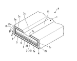
- FIG. 1 is a perspective view showing a cross section of an oxide superconducting wire according to an embodiment of the present invention.
- the oxide superconducting wire A according to this embodiment includes a tape-shaped oxide superconducting laminate 1 and a metal tape 2 made of a conductive material such as copper and covering the oxide superconducting laminate 1.
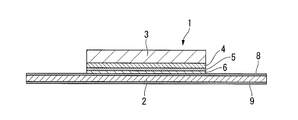
- the oxide superconducting laminate 1 has a tape-like base material 3, an intermediate layer 4, an oxide superconducting layer 5, and a protective layer 6.
- the intermediate layer 4, the oxide superconducting layer 5, and the protective layer 6 are laminated on the base material 3 in this order.
- each component of the oxide superconducting laminate 1 will be described in detail with reference to FIG.
- the base material 3 may be any material that can be used as a base material for a normal oxide superconducting wire, and is preferably a long tape having flexibility. Moreover, as a material of the base material 3, what has high mechanical strength, heat resistance, and has the metal which can be easily processed into a wire is preferable. Examples of such materials include various heat-resistant metal materials such as nickel alloys such as stainless steel and hastelloy, or materials obtained by arranging ceramics on these various metal materials. Among them, Hastelloy (trade name, manufactured by Haynes, USA) is preferable as a commercial product.
- Hastelloy such as Hastelloy B, C, G, N, and W, which have different amounts of components such as molybdenum, chromium, iron, and cobalt. Any kind of Hastelloy can be used for the substrate 3.
- the base material 3 an oriented Ni—W alloy tape base material in which a texture is introduced into a nickel alloy can also be employed.
- the thickness of the substrate 3 may be appropriately adjusted according to the purpose, and is usually 10 to 500 ⁇ m, preferably 20 to 200 ⁇ m.
- the intermediate layer 4 may have a structure in which a diffusion prevention layer, a bed layer, an alignment layer, and a cap layer are stacked in this order.
- a diffusion prevention layer As a result of the heat treatment of the other layers formed on this layer, when the base material 3 or other layers receive a thermal history, a part of the constituent elements of the base material 3 diffuses. , And has a function of suppressing entry into the oxide superconducting layer 5 side as an impurity.
- the specific structure of the diffusion preventing layer is not particularly limited as long as it can exhibit the above function.
- the bed layer is used to suppress the reaction of constituent elements at the interface between the base material 3 and the oxide superconducting layer 5 and to improve the orientation of the layer provided on this layer.
- the specific structure of the bed layer is not particularly limited as long as it can exhibit the above functions.
- a multi-layer bed layer is desirable.
- the alignment layer controls the crystal orientation of the cap layer and the oxide superconducting layer 5 formed thereon, suppresses the constituent elements of the base material 3 from diffusing into the oxide superconducting layer 5, and has a thermal expansion. It has a function of relaxing the difference between the base material 3 and the oxide superconducting layer 5 in physical properties such as the rate and the lattice constant.
- the material of the alignment layer is not particularly limited as long as it can exhibit the above functions, but metal oxides such as Gd 2 Zr 2 O 7 , MgO, ZrO 2 —Y 2 O 3 (YSZ) are particularly suitable. .
- a layer having high crystal orientation can be obtained in an ion beam assisted vapor deposition method (hereinafter also referred to as IBAD method) described later.
- IBAD method ion beam assisted vapor deposition method
- the cap layer strongly controls the crystal orientation of the oxide superconducting layer 5 to be equal to or higher than that of the oriented layer, diffuses the elements constituting the oxide superconducting layer 5 into the intermediate layer 4, and the oxide superconducting layer 5.
- the material of the cap layer is not particularly limited as long as it can express the above function, but CeO 2 , LaMnO 3 , Y 2 O 3 , Al 2 O 3 , Gd 2 O 3 , ZrO 2 , Ho 2 O 3 , Metal oxides such as Nd 2 O 3 and Zr 2 O 3 are preferable from the viewpoint of lattice matching with the oxide superconducting layer 5.
- the cap layer may include a Ce—M—O-based oxide in which part of Ce is substituted with another metal atom or metal ion.
- the oxide superconducting layer 5 has a function of flowing current when in the superconducting state.
- an oxide superconductor material having a generally known composition can be widely used. Examples thereof include copper oxide superconductors such as RE-123 series superconductors and Bi series superconductors.
- the composition of the RE-123 series superconductor is, for example, REBa 2 Cu 3 O (7-x) (RE represents a rare earth element such as Y, La, Nd, Sm, Er, Gd, and x represents oxygen deficiency). Specific examples include Y123 (YBa 2 Cu 3 O (7-x) ) and Gd123 (GdBa 2 Cu 3 O (7-x) ).
- Examples of the composition of the Bi-based superconductor include Bi 2 Sr 2 Cann -1 Cu n O 4 + 2n + ⁇ (n represents the number of CuO 2 layers, and ⁇ represents excess oxygen).
- this copper oxide superconductor an oxide superconductor exhibiting superconducting characteristics with a well-structured crystal structure can be obtained by incorporating oxygen into the base material, which is an insulator, by oxygen annealing treatment.
- the material of the oxide superconducting layer 5 used in the present embodiment is a copper oxide superconductor. Unless otherwise specified, the material used for the oxide superconducting layer 5 is a copper oxide superconductor.
- the protective layer 6 bypasses an overcurrent (accident current) that occurs in the event of an abnormality (for example, a short circuit due to a lightning strike) together with the stabilization layer 10 described later, or a layer provided on the oxide superconducting layer 5 and this layer.
- an overcurrent an abnormal current
- the stabilization layer 10 described later
- a layer provided on the oxide superconducting layer 5 and this layer To suppress the chemical reaction that occurs between the layers, or to prevent the deterioration of superconducting properties caused by the breakdown of the composition of some of the elements in one of the stacked layers entering the other layer. It has a function.
- the protective layer 6 is preferably formed from a material containing at least Ag, such as Ag or an Ag alloy.
- the protective layer 6 is provided only on the upper surface of the oxide superconducting layer 5, but is not limited thereto.
- the protective layer 6 is formed by a film forming method such as a sputtering method, a thin layer of Ag is formed on the side surfaces of the base material 3, the intermediate layer 4, and the oxide superconducting layer 5 and the back surface of the base material 3 by the wrapping of Ag particles.
- a film forming method such as a sputtering method
- a thin layer of Ag is formed on the side surfaces of the base material 3, the intermediate layer 4, and the oxide superconducting layer 5 and the back surface of the base material 3 by the wrapping of Ag particles.
- such a configuration may be adopted.
- the thickness D of the protective layer 6 formed on the oxide superconducting layer 5 can be 5 ⁇ m or less.
- the thickness D of the protective layer 6 is a thin layer of 5 ⁇ m or less, cost can be reduced.
- the film thickness D of the protective layer 6 is 1 micrometer or more.
- the thickness D of the protective layer 6 is less than 1 ⁇ m, Ag may aggregate during the oxygen annealing treatment of the protective layer 6 and the oxide superconducting layer 5 may be exposed from the protective layer 6.
- the oxide superconducting laminate 1 is configured as described above.
- the oxide superconducting wire A in which the outer periphery of the oxide superconducting laminate 1 is covered with the metal tape 2 will be described in detail with reference to FIG.
- Covering the surface and both side surfaces of the protective layer 6, both side surfaces of the oxide superconducting layer 5 thereunder, both side surfaces of the intermediate layer 4, both side surfaces of the base material 3, and part of the back surface side of the base material 3 A metal tape 2 made of a conductive material such as copper is provided, and the metal tape 2 constitutes the stabilization layer 10.
- the stabilization layer 10 functions as a bypass that commutates current together with the protective layer 6 when the oxide superconducting layer 5 transitions from the superconducting state to the normal conducting state.
- solder layers (low melting point metal layers) 7 are formed on both the front and back surfaces of the metal tape 2.
- the solder layer 7 includes an outer coating layer 7a that covers the outer surface of the metal tape 2, an inner coating layer 7b that is in close contact with the inner surface of the metal tape 2 and covers the periphery of the oxide superconducting laminate 1, and the metal tape 2 And a covering portion 7c covering both ends in the width direction.
- the metal tape 2 is bent in a substantially C shape in cross section, has a front wall 2a, a side wall 2b, and back walls 2c, 2c, and extends from the front surface of the protective layer 6 to the back surface of the base material 3.
- the oxide superconducting laminate 1 is covered so that a part of the back surface of the oxide is superposed.
- the metal tape 2 covers the upper surface and both side surfaces of the protective layer 6, both side surfaces of the oxide superconducting layer 5, both side surfaces of the intermediate layer 4, both side surfaces of the base material 3, and part of the back surface of the base material 3.
- the inner coating layer 7 b of the solder layer 7 is formed so as to completely fill the space between the metal tape 2 and the oxide superconducting laminate 1 in the entire peripheral surface of the oxide superconducting laminate 1.
- the solder layer (low melting point metal layer) 7 is formed of solder in this embodiment, but the low melting point metal layer may be made of a metal having a melting point of 240 to 400 ° C., for example, Sn, Sn alloy, indium or the like. good.
- solder As the solder, Sn—Pb, Pb—Sn—Sb, Sn—Pb—Bi, Bi—Sn, Sn—Cu, Sn—Pb—Cu, Sn—Ag, etc. are used. Also good. Note that if the melting point of the solder layer 7 is high, the superconducting properties of the oxide superconducting layer 5 are adversely affected when the solder layer 7 is melted. Therefore, the melting point of the solder layer 7 is preferably low. Specifically, a material having a melting point of 350 ° C. or lower, more preferably around 240 to 300 ° C. is desirable.
- the thickness of the solder layer 7 is preferably in the range of 1 ⁇ m to 10 ⁇ m, more preferably in the range of 2 ⁇ m to 6 ⁇ m.
- the thickness of the solder layer 7 is less than 1 ⁇ m, there is a possibility that the gap between the oxide superconducting laminate 1 and the metal tape 2 cannot be completely filled and the gap remains, and further, the solder is melted. During this, the constituent elements of the solder layer 7 may diffuse to form an alloy layer between the metal tape 2 or the Ag protective layer 6.
- the thickness of the solder layer 7 exceeds 10 ⁇ m, the solder that protrudes from the front end side of the back wall 2c of the metal tape 2 when the solder is melted and soldered by heating and pressing with a roll as will be described later.
- the amount increases.
- the thickness of the covering portion 7c is increased, which causes a turbulence when the oxide superconducting wire A is wound.
- the solder layer 7 filled between the oxide superconducting laminate 1 and the surrounding metal tape 2 covers the periphery of the oxide superconducting laminate 1, so that the metal It is possible to prevent moisture from entering the oxide superconducting laminate 1 located inside the tape 2 from the outside.
- a tape-shaped oxide superconducting laminate in which a substrate 3, an intermediate layer 4, an oxide superconducting layer 5, and a protective layer 6 are laminated.
- a body 1 is prepared, and a metal tape 2 is disposed under the protective layer 6 of the oxide superconducting laminate 1.
- Solder layers 8 and 9 are formed on the front and back surfaces of the metal tape 2 used here by plating.
- the thickness of the solder layers 8 and 9 is preferably in the range of 1 ⁇ m to 10 ⁇ m, more preferably in the range of 2 ⁇ m to 6 ⁇ m.
- both ends of the metal tape 2 along the both side surfaces of the substrate 3 are formed using a forming roll or the like as shown in FIG. 3B. Bend the part upward. Thereafter, as shown in FIG. 3C, the metal tape 2 is further bent along the upper surface of the substrate 3. As described above, the metal tape 2 is bent so as to be substantially C-shaped in the cross section.
- (Modification) 4 and 5 are cross-sectional views of oxide superconducting wires B and C, which are modifications of the oxide superconducting wire A according to the above-described embodiment.
- the oxide superconducting wire B according to this modification the tape-shaped oxide superconducting laminate 1 is covered with the metal tape 2 as in the oxide superconducting wire A according to the above embodiment.
- the oxide superconducting wires B and C according to this modification are different from the oxide superconducting wire A according to the above embodiment in that the gap portion between the front edges of the back walls 2c and 2c of the C-shaped metal tape 2 is used.
- 11 is embedded in an embedded layer 17 c made of a solder layer (low melting point metal layer) 17.
- the inner coating layer 17 a of the solder layer (low melting point metal layer) 17 is formed only on the inner peripheral surface of the metal tape 2.
- the oxide superconducting wires B and C shown in FIGS. 4 and 5 the structure other than the above is the same as that of the oxide superconducting wire A, and the same components are denoted by the same reference numerals and the description thereof is omitted. .
- the gap between the oxide superconducting laminate 1 and the metal tape 2 is filled with the inner coating layer 17a, and the back wall 2c of the metal tape 2 is formed.
- the gap between 2c is filled with the buried layer 17c.
- the buried layer 17 c suppresses the intrusion of moisture into the oxide superconducting laminate 1, and in particular prevents the ingress of moisture into the oxide superconducting layer 5 inside the metal tape 2. Even in the structure in which the solder layer 17 is provided on the inner surface of the metal tape 2 without providing the solder layer on the outer surface of the metal tape 2 as in the oxide superconducting wire B, the moisture is introduced into the interior. Intrusion can be prevented.
- a sufficient amount of solder is supplied to fill the gap between the back walls 2c, 2c of the metal tape 2 to fill the embedded layer 17c.
- the oxide superconducting wires B and C can be obtained by forming. Further, a thick solder layer is formed on the surface of the metal tape 2 in advance, the solder layer is melted by heating, and the melted solder is pressed between the back walls 2c and 2c of the metal tape 2 using a pressure roll.
- the buried layer 17c may be formed by oozing from the surface.
- the resistance value R of the oxide superconducting wire A in the normal conducting state is preferably in the range represented by the following formula (1).
- V represents a voltage
- Ic represents a critical current value of the oxide superconducting wire A.
- ⁇ is a coefficient by which the critical current value Ic is multiplied.
- a current of 1.5 to 3 times the critical current value Ic is required. That is, when the oxide superconducting layer 5 transitions from the superconducting state to the normal conducting state, a current 1.5 to 3 times the critical current value Ic flows through the stabilization layer 10 and the protective layer 6. Therefore, the coefficient ⁇ of 1.5 to 3 is multiplied by the critical current value Ic.
- the critical current value Ic of the oxide superconducting layer 5 can be set by its cross-sectional area.
- the assumed critical current value Ic is in the range of 50 to 1000A.
- the voltage drop of the oxide superconducting wire A having a width of 1 cm and a length of 1 cm in the normal conducting state needs to be in the range of 0.3 to 5V.
- the desirable range of the resistance value R in the normal conduction state of the oxide superconducting wire A is calculated. can do. That is, by substituting each value of 0.3 V for the voltage V, 1000 A for the critical current value Ic, and 3 for the coefficient ⁇ into the equation (1), the lower limit value of 100 ⁇ can be calculated. Further, by substituting each value of 5 V for the voltage V, 50 A for the critical current value Ic, and 1.5 for the coefficient ⁇ into the equation (1), the upper limit value 66.667 m ⁇ of the resistance value can be calculated.
- the oxide superconducting wire A is cooled to about 90K with liquid nitrogen or the like when used.
- the above-described resistance value R is a resistance value at the temperature during use.
- the resistance value at room temperature (20 ° C.) of a normal conductive material of a copper alloy (brass as an example) is about 1.5 times the resistance value at 90 K. Therefore, the resistance value of the oxide superconducting wire A at room temperature is A desirable range is 150 ⁇ or more and 100 m ⁇ or less. Since the resistance value of the oxide superconducting wire is inversely proportional to its width, a desirable range of the resistance value is determined according to the width of the oxide superconducting wire. For example, the desirable range of the resistance value at room temperature of an oxide superconducting wire of 5 mm width and 1 cm length is 300 ⁇ or more and 200 m ⁇ or less.
- the resistance value of the oxide superconducting wire A in the normal conducting state is that the resistance value of the oxide superconducting layer 5 is close to the resistance value in the insulating state, so that the protective layer 6 and the solder layer (low melting point metal layer) 7 and 17 and the combined resistance of the stabilization layer 10.
- the resistance values of the solder layers 7 and 17 are sufficiently larger than the resistance values of the protective layer 6 and the stabilization layer 10 in consideration of the thinness (that is, the cross-sectional area) and the volume resistivity. That is, since almost no current flows through the solder layers 7 and 17, the solder layers 7 and 17 can be ignored in calculating the resistance value. Therefore, the resistance value in the normal conducting state of the oxide superconducting wire A can be approximated by the combined resistance of the protective layer 6 and the stabilizing layer 10.
- the protective layer 6 is made of Ag or an Ag alloy. Cost reduction can be achieved by using the protective layer 6 having a film thickness D of 5 ⁇ m or less. Moreover, it is preferable that the film thickness D of the protective layer 6 is 1 micrometer or more.
- the resistance value of the stabilization layer 10 can be variously adjusted using the thickness d of the stabilization layer 10 and the volume resistivity of the material constituting the stabilization layer 10 as parameters. Therefore, the thickness d of the stabilization layer 10 and the stabilization layer 10 are configured so that the resistance value at room temperature of the oxide superconducting wire A having the protective layer 6 having a thickness of 1 ⁇ m to 5 ⁇ m is within the above range.
- the material to be selected may be selected.
- the metal tape 2 When a material having a low volume resistivity is used as the material of the stabilization layer 10, it is necessary to use the thin stabilization layer 10. However, in the case where the metal tape 2 is formed on the oxide superconducting laminate 1 as the stabilizing layer 10, if the thickness d of the metal tape 2 is too thin, the metal tape 2 may be broken. Furthermore, as described above, when the metal tape 2 is bent in a C shape and is formed so as to cover the oxide superconducting laminate 1, tearing is more likely to occur. On the other hand, when a material having a high volume resistivity is used as the material of the stabilization layer 10, it is necessary to use the thick stabilization layer 10. However, if the stabilization layer 10 is thick, the thickness dimension of the oxide superconducting wire A itself is enlarged accordingly.
- the metal tape 2 when the metal tape 2 is bent in a C shape and is formed so as to cover the oxide superconducting laminate 1, it is very difficult to form the metal tape 2 having a thickness exceeding 60 ⁇ m. In addition, since it is necessary to apply high stress to the metal tape 2 during molding, the oxide superconducting layer 5 may be deteriorated.
- the thickness d of the stabilizing layer 10 is preferably 9 ⁇ m or more and 60 ⁇ m or less. Further, in this thickness d range, the volume resistivity of the stabilizing layer 10 at which the resistance value of the oxide superconducting wire A is 150 ⁇ or more and 100 m ⁇ or less is 3.8 ⁇ ⁇ cm or more and 15 ⁇ ⁇ cm or less. More preferably, it is 3.8 ⁇ ⁇ cm or more and 9.6 ⁇ ⁇ cm or less.
- the metal tape 2 copper nickel alloy (GCN15, GCN10, GCN5: corresponding standard JIS C 2532), Corson alloy, brass (Cu—Zn alloy),
- Examples include beryllium copper and phosphor bronze.
- Table 1 shows the relationship between the film thickness of the protective layer 6 and the film thickness of the stabilization layer 10 when a Corson alloy (C7025) having a volume resistivity of 3.8 ⁇ ⁇ cm is used as the material of the stabilization layer 10.
- the resistance value at room temperature (normal conducting state) of the oxide superconducting wire is shown.
- Table 2 shows the relationship between the thickness of the protective layer 6 and the thickness of the stabilization layer 10 when a copper nickel alloy (GCN15) having a volume resistivity of 15 ⁇ ⁇ cm is used as the material of the stabilization layer 10.
- GCN15 copper nickel alloy
- the thickness of the stabilization layer 10 is 9.4 to By adjusting in the range of 12.0 ⁇ m, a preferable combined resistance value (that is, the resistance value of the oxide superconducting wire at normal temperature) can be obtained.
- a preferable combined resistance value that is, the resistance value of the oxide superconducting wire at normal temperature
- the thickness of the stabilization layer 10 is 9.4 to 58 ⁇ m with respect to the thickness 1 to 5 ⁇ m of the protective layer 6.
- FIG. 6 shows a superconducting fault current limiter 99 using the above-described oxide superconducting wire A (or B, C).
- the oxide superconducting wire A (B, C) is wound on a winding drum over a plurality of layers to constitute a superconducting current limiting module 90.
- the superconducting fault current limiter module 90 is stored in a liquid nitrogen container 95 filled with liquid nitrogen 98.
- the liquid nitrogen container 95 is stored inside a vacuum container 96 that blocks heat from the outside.
- a liquid nitrogen filling part 91 and a refrigerator 93 are provided on the upper part of the liquid nitrogen container 95. Below the refrigerator 93, a thermal anchor 92 and a hot plate 97 are provided.
- the superconducting current limiter 99 has a current lead portion 94 for connecting the superconducting current limiter module 90 and an external power source (not shown).
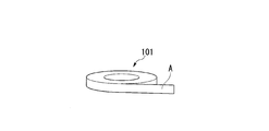
- FIG. 7B shows a pancake coil 101 using the above-described oxide superconducting wire A (B, C).
- the oxide superconducting wire A can constitute a wound pancake coil 101.
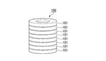
- the superconducting coil 100 which emits the strong magnetic force shown to FIG. 7A can be formed by laminating
- the oxide superconducting wires A, B, and C can be used for various superconducting devices.
- the superconducting device is not particularly limited as long as it has the oxide superconducting wire A, and includes, for example, a superconducting cable, a superconducting motor, a superconducting transformer, a superconducting current limiter, a superconducting power storage device, and the like.
- Example preparation An Al 2 O 3 layer (diffusion prevention layer; film thickness: 150 nm) was formed by sputtering on a tape-shaped Hastelloy (trade name, manufactured by Haynes, USA) having a width of 5 mm and a thickness of 0.1 mm. On this diffusion prevention layer, a Y 2 O 3 layer (bed layer; film thickness: 20 nm) was formed by ion beam sputtering.
- an MgO layer (metal oxide layer; film thickness: 10 nm) is formed on the bed layer by an ion beam assisted deposition method (IBAD method), and a pulse laser deposition method (PLD method) is formed on the metal oxide layer.
- IBAD method ion beam assisted deposition method
- PLD method pulse laser deposition method
- a 2.0 ⁇ m thick GdBa 2 Cu 3 O 7- ⁇ oxide superconducting layer
- a 5 ⁇ m thick Ag layer (protective layer) is formed on the oxide superconducting layer by a sputtering method. ) was formed.
- a metal tape having a width of 10 mm subjected to Sn solder plating was formed on both surfaces of the protective layer so as to form a substantially C shape in the cross section, and the peripheral surface of the oxide superconducting laminate was covered with the metal tape. Thereafter, Sn solder was melted by heating to form a solder layer so that a metal tape was deposited on the peripheral surface of the oxide superconducting laminate.
- a metal tape having the thickness and material shown in Table 3 was used. Oxide superconducting wires of Examples 1 to 6 and Comparative Examples 1 and 2 were produced by the above process.
- the oxide superconducting wires of Examples 1 to 6 and Comparative Example 12 were subjected to a pressure cooker test that was allowed to stand for 100 hours under high temperature (120 ° C.), high humidity (100%), and high pressure (0.2 MPa). The ratio of critical current values before and after was measured.
- Table 3 shows the percentage of the ratio of the critical current value (Ic) after standing to the critical current value (Ic 0 ) before standing as moisture deterioration.
- the oxide superconducting wires of Examples 1 to 6 and Comparative Examples 1 and 2 were each cut to a length of 10 cm, and an excessive current equivalent to the current at the time of abnormality assumed between the ends of each wire was applied. .
- Current waveforms from immediately after application of current to the sixth wave were observed, and it was confirmed for each wire whether or not the current limiting effect was obtained.
- the results are shown in Table 3.
- “ ⁇ ” indicates that the metal tape can be formed
- “X” indicates that the metal tape cannot be formed.
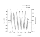
- FIG. 8 shows a current waveform observed when an excessive current equivalent to the accident current assumed in the oxide superconducting wire of Example 2 is applied.
- a metal tape could not be formed so as to cover the oxide superconducting laminate.
- the metal tape since the thickness of the oxygen-free copper foil used as the metal tape is as thin as 5 ⁇ m, the metal tape is broken when the metal tape is formed into a C shape, and the oxide superconducting laminate is formed. could not be coated.
- the white used as the metal tape had high rigidity and the foil thickness was as thick as 96 ⁇ m, so that the white metal tape could not be formed into a C shape.
- the oxide superconducting wires of Examples 1 to 6 were not deteriorated by the pressure cooker test. Further, the oxide superconducting wires of Examples 1 to 6 and Comparative Examples 1 and 2 all showed good current limiting characteristics.
- FIG. 8 showing the current waveform observed for the wire of Example 2, it can be seen that the current value is gradually suppressed from the first wave.
- the oxide superconducting wire according to the example of the present invention exhibits good current limiting characteristics.
- the periphery of the oxide superconducting laminate is covered with a metal tape having a predetermined thickness, so that deterioration due to moisture does not occur even in severe conditions. confirmed.
- an oxide superconducting wire used for a superconducting current limiting device which exhibits stable current limiting characteristics while preventing burning even when the protective layer is formed thin.
Landscapes
- Engineering & Computer Science (AREA)
- Chemical & Material Sciences (AREA)
- Organic Chemistry (AREA)
- Ceramic Engineering (AREA)
- Power Engineering (AREA)
- Inorganic Chemistry (AREA)
- Manufacturing & Machinery (AREA)
- Superconductors And Manufacturing Methods Therefor (AREA)
- Inorganic Compounds Of Heavy Metals (AREA)
- Containers, Films, And Cooling For Superconductive Devices (AREA)
- Emergency Protection Circuit Devices (AREA)
Abstract
Description
本願は、2012年12月28日に、日本に出願された特願2012-288302号に基づき優先権を主張し、その内容をここに援用する。
Agは高価な材料であるため、Agを含む保護層を更に薄くすることが求められている。保護層はAg又はAg合金からなり、安定化層に対して体積抵抗率が著しく低い。保護層の厚みを薄くすると、これを補完するために安定化層の厚みを大幅に厚くする必要があるため、酸化物超電導線材の厚み寸法が肥大化してしまう。酸化物超電導線材の厚み寸法が肥大化すると、酸化物超電導線材を巻いて形成したコイルの磁界密度を大きくすることができなくなる。
前記第一の態様によれば、Ag又はAg合金からなる保護層の膜厚が5μm以下であるため、酸化物超電導線材に使用するAgの使用量を減らすことができ、その結果、コストを抑えることができる。加えて、金属テープの室温での体積抵抗率が3.8μΩ・cm以上15μΩ・cm以下であるため、前記酸化物超電導線材が用いられた超電導限流器において、保護層の膜厚が5μm以下であっても、臨界電流の1.5~3倍の過大な電流が印加された場合にその電流を抑制することができ、その結果、酸化物超電導線材の焼損を防止でき、安定した限流特性を発揮することができる。
前記第二の態様によれば、Ag又はAg合金からなる保護層の膜厚が5μm以下であるため、酸化物超電導線材に使用するAgの使用量を減らすことができ、その結果、コストを抑えることができる。加えて、酸化物超電導線材の1cm幅、1cm長さにおける室温での抵抗値が150μΩ以上100mΩ以下であるため、前記酸化物超電導線材が用いられた超電導限流器において、保護層の膜厚が5μm以下であっても、臨界電流の1.5~3倍の過大な電流が印加された場合にその電流を抑制することができ、その結果、酸化物超電導線材の焼損を防止でき、安定した限流特性を発揮することができる。
この場合、酸化物超電導積層体の外周が金属テープにより覆われているため、水分の浸入による酸化物超電導層の劣化を防ぐことができる。
この場合、安定化層の厚みが9μm以上60μm以下である。即ち、酸化物超電導積層体を覆う金属テープの厚みが9μm以上60μm以下である。厚みが9μm以上の金属テープを用いることにより、酸化物超電導積層体を金属テープにより覆う際に金属テープが破れてしまうことを防ぐことができる。また、厚みが60μm以下の金属テープを用いることにより、金属テープの成形が容易となり、酸化物超電導積層体を確実に覆うことができる。
本発明の第四の態様に係る超電導限流器は、上記酸化物超電導線材を備える。
本発明の第五の態様に係る超電導機器は、上記酸化物超電導線材を備える。
前記酸化物超電導線材を超電導コイル、超電導限流器、その他の超電導機器に用いることで、水分に対する超電導機器の保護性能を向上させることが可能となる。また、酸化物超電導線材に過大な電流が流れた際に酸化物超電導線材が焼損することを防ぐことができる。したがって、従来よりも高い信頼性を有する超電導機器を実現することが可能となる。
図1は、本発明の一実施形態に係る酸化物超電導線材の断面を示す斜視図である。この実施形態に係る酸化物超電導線材Aは、テープ状の酸化物超電導積層体1と、銅などの導電性材料からなり酸化物超電導積層体1を覆う金属テープ2とを備えている。
酸化物超電導積層体1は、図2に示すように、テープ状の基材3と、中間層4と、酸化物超電導層5と、保護層6とを有している。中間層4、酸化物超電導層5、及び保護層6は、基材3上にこの順で積層されている。
以下、図2を基に、酸化物超電導積層体1の各構成要素に関して詳細に説明する。
拡散防止層は、この層の上に形成される他の層が加熱処理された結果、基材3や他の層が熱履歴を受ける場合に、基材3の構成元素の一部が拡散し、不純物として酸化物超電導層5側に混入することを抑制する機能を有する。拡散防止層の具体的な構造は、上記機能を発現し得るものであれば特に限定されない。不純物の混入を防止する効果が比較的高いAl2O3、Si3N4、又はGZO(Gd2Zr2O7)等から構成される単層構造あるいは複層構造の拡散防止層が望ましい。
キャップ層の材料は、上記機能を発現し得るものであれば特に限定されないが、CeO2、LaMnO3、Y2O3、Al2O3、Gd2O3、ZrO2、Ho2O3、Nd2O3、Zr2O3等の金属酸化物が、酸化物超電導層5との格子整合性の観点から好適である。これらのなかでも、酸化物超電導層5とのマッチング性の観点から、CeO2、LaMnO3が特に好適である。
キャップ層にCeO2を用いる場合、キャップ層は、Ceの一部が他の金属原子又は金属イオンで置換されたCe-M-O系酸化物を含んでいても良い。
本実施形態おいて用いられる酸化物超電導層5の材料は、銅酸化物超電導体であり、以下、特に指定がなければ、酸化物超電導層5に用いる材料を銅酸化物超電導体とする。
このため、保護層6は、AgあるいはAg合金のような少なくともAgを含む材料から形成されることが好ましい。
なお、図1及び図2において、保護層6は、酸化物超電導層5の上面のみに設けられているが、これに限られない。スパッタ法などの成膜法により保護層6を形成した場合、基材3、中間層4、酸化物超電導層5の側面並びに基材3の裏面にAg粒子の回り込みによるAgの薄い層が形成されることがあるが、係る構成を採用していても良い。
以上のように酸化物超電導積層体1が構成される。
保護層6の表面と両側面、及びその下の酸化物超電導層5の両側面、中間層4の両側面、基材3の両側面、並びに基材3の裏面側の一部を覆うように銅などの導電性材料からなる金属テープ2が設けられ、当該金属テープ2が安定化層10を構成している。
安定化層10は、酸化物超電導層5が超電導状態から常電導状態に転移した時に、保護層6とともに、電流を転流するバイパスとして機能する。
金属テープ2は、横断面において略C字形に折り曲げられ、表面壁2aと側壁2bと裏面壁2c、2cとを有し、保護層6の表面から基材3の裏面に亘って、基材3の裏面の一部が露出するように酸化物超電導積層体1を覆っている。即ち、金属テープ2は、保護層6の上面と両側面、酸化物超電導層5の両側面、中間層4の両側面、基材3の両側面、基材3の裏面の一部を覆っている。
半田層7の内側被覆層7bは、酸化物超電導積層体1の全周面のうち、金属テープ2と酸化物超電導積層体1の間を完全に埋めるように形成されている。
半田層(低融点金属層)7は、本実施形態では半田から形成されているが、低融点金属層として、融点240~400℃の金属、例えば、Sn、Sn合金、インジウム等からなるものでも良い。上記半田として、Sn-Pb系、Pb-Sn-Sb系、Sn-Pb-Bi系、Bi-Sn系、Sn-Cu系、Sn-Pb-Cu系、Sn-Ag系などの半田を用いても良い。なお、半田層7の融点が高いと、半田層7を溶融させる際に酸化物超電導層5の超電導特性に悪影響を及ぼすので、半田層7の融点は低い方が好ましい。具体的には、350℃以下、より好ましくは240~300℃前後の融点を有する材料が望ましい。
酸化物超電導積層体1の中央と金属テープ2の中央とを位置合わせした後、フォーミングロールなどを用いて、図3Bに示すように、基材3の両側面に沿うように金属テープ2の両端部を上方に折り曲げる。その後、図3Cに示すように、基材3の上面に沿うように金属テープ2をさらに折り曲げる。以上のように、横断面において略C字形となるように金属テープ2を折り曲げ加工する。
この処理により、溶融した半田層8、9は酸化物超電導積層体1と金属テープ2との間の間隙を完全に埋めるように拡がり、その間隙を充填する。この後、全体を冷却し、半田を固化させると、図3Cに示すように、半田層7を備えた図1に示す構造と同等の構造を有する酸化物超電導線材Aを得ることができる。
図4、図5は、上述の実施形態に係る酸化物超電導線材Aの変形例である酸化物超電導線材B、Cの横断面図である。この変形例に係る酸化物超電導線材Bでは、上記実施形態に係る酸化物超電導線材Aと同様、テープ状の酸化物超電導積層体1が金属テープ2で覆われている。
本変形例に係る酸化物超電導線材B、Cが上記実施形態に係る酸化物超電導線材Aと異なっているのは、C字形の金属テープ2の裏面壁2c、2cの先端縁の間の間隙部分11が半田層(低融点金属層)17からなる埋込層17cにより埋め込まれている点である。また、酸化物超電導線材Bにおいては、金属テープ2の内周面のみに半田層(低融点金属層)17の内側被覆層17aが形成されている。
図4、図5に示す酸化物超電導線材B、Cにおいて、上記以外の構造は酸化物超電導線材Aと同様であり、同一の構成要素については同一の符号を付し、それらの説明を省略する。
次に上述した本発明の実施形態に係る酸化物超電導線材A(B、C)の電気的な特性について説明する。
酸化物超電導線材Aを超電導限流器に使用する場合において、酸化物超電導線材Aの常電導状態での抵抗値Rは、以下に示す式(1)で表される範囲にあることが好ましい。

また、限流特性を得るためには、常電導状態での1cm幅1cm長さの酸化物超電導線材Aの電圧降下は0.3~5Vの範囲であることが必要である。
安定化層10の抵抗値は、安定化層10の厚さdと安定化層10を構成する材料の体積抵抗率とをパラメーターとして様々に調整することができる。したがって、膜厚が1μm以上5μm以下の保護層6を有する酸化物超電導線材Aの室温での抵抗値が上記の範囲となるように、安定化層10の厚さdと安定化層10を構成する材料とを選択すればよい。
これに対して、体積抵抗率が高い材料を安定化層10の材料として使用する場合は、厚い安定化層10を用いる必要がある。しかしながら、安定化層10が厚いと酸化物超電導線材A自体の厚み寸法もそれに伴い肥大化してしまう。また、上述したように金属テープ2をC字形に曲げて、酸化物超電導積層体1を覆うように成形する場合において、厚さ60μmを超えた金属テープ2を成形することは非常に困難であるのみならず、成形時に高い応力を金属テープ2に加える必要があるため酸化物超電導層5が劣化する可能性がある。
このような体積抵抗率を満たす安定化層10、即ち金属テープ2の材料としては、銅ニッケル合金(GCN15、GCN10、GCN5:対応規格JIS C 2532)、コルソン合金、黄銅(Cu-Zn合金)、ベリリウム銅、リン青銅等が挙げられる。
また、表2に、安定化層10の材料として体積抵抗率15μΩ・cmの銅ニッケル合金(GCN15)を用いた場合の、保護層6の膜厚と安定化層10の膜厚との関係、及び酸化物超電導線材の室温(常電導状態)における抵抗値を示す。


これらのことから、安定化層10の体積抵抗率が3.8~15μΩ・cmである場合、保護層6の膜厚1~5μmに対して安定化層10の厚さを9.4~58μmの範囲で調整することにより、常温において好ましい抵抗値を有する酸化物超電導線材を得ることができる。
図6に、上述の酸化物超電導線材A(又はB、C)を用いた超電導限流器99を示す。
超電導限流器99において、酸化物超電導線材A(B、C)は巻胴に複数層に渡って巻回されて超電導限流器用モジュール90を構成している。超電導限流器用モジュール90は、液体窒素98が充填された液体窒素容器95に格納されている。液体窒素容器95は、外部からの熱を遮断する真空容器96の内部に格納されている。
液体窒素容器95の上部には、液体窒素充填部91と冷凍機93とが設けられている。冷凍機93の下方には、熱アンカー92と熱板97とが設けられている。
また、超電導限流器99は、超電導限流器用モジュール90と外部電源(図示略)とを接続するための電流リード部94を有する。
図7Bに、上述の酸化物超電導線材A(B、C)を用いたパンケーキコイル101を示す。酸化物超電導線材Aは、巻回しパンケーキコイル101を構成することができる。また複数のパンケーキコイル101を積層し互いに接続することにより、図7Aに示す強力な磁力を発する超電導コイル100を形成することができる。
(試料の作製)
幅5mm、厚さ0.1mmのテープ状のハステロイ(米国ヘインズ社製商品名)製の基材上に、スパッタ法によりAl2O3層(拡散防止層;膜厚150nm)を成膜し、この拡散防止層上に、イオンビームスパッタ法によりY2O3層(ベッド層;膜厚20nm)を成膜した。次いで、このベッド層上に、イオンビームアシスト蒸着法(IBAD法)によりMgO層(金属酸化物層;膜厚10nm)を形成し、この金属酸化物層上にパルスレーザー蒸着法(PLD法)により0.5μm厚のCeO2(キャップ層)を成膜した。次いでこのキャップ層上にPLD法により2.0μm厚のGdBa2Cu3O7-δ(酸化物超電導層)を形成し、この酸化物超電導層上にスパッタ法により5μm厚のAg層(保護層)を形成した。さらに、この保護層の両面に、Sn半田めっきを施した幅10mmの金属テープを横断面において略C字形をなすようにフォーミングし、酸化物超電導積層体の周面を金属テープで覆った。その後、Sn半田を加熱により溶融させて酸化物超電導積層体の周面に金属テープが被着するように半田層を形成した。表3に示す厚さ及び材質を有する金属テープを用いた。以上のプロセスによって、実施例1~6及び比較例1、2の酸化物超電導線材を作製した。
また、限流特性として、異常時の過大な電流の抑制効果を以下のように確認した。実施例1~6及び比較例1、2の酸化物超電導線材をそれぞれ10cmの長さに切断し、それぞれの線材の端部間に想定される異常時の電流と同等の過大な電流を印加した。電流を印加した直後から第6波までの電流波形を観察し、限流効果が得られるか否かをそれぞれの線材について確認した。その結果を表3に示す。なお、表中の「○」は金属テープが成形可能であることを、「×」は金属テープが成形不能であることを示す。また、一例として、実施例2の酸化物超電導線材に想定される事故電流と同等の過大な電流を印加した際に観察された電流波形を図8に示す。
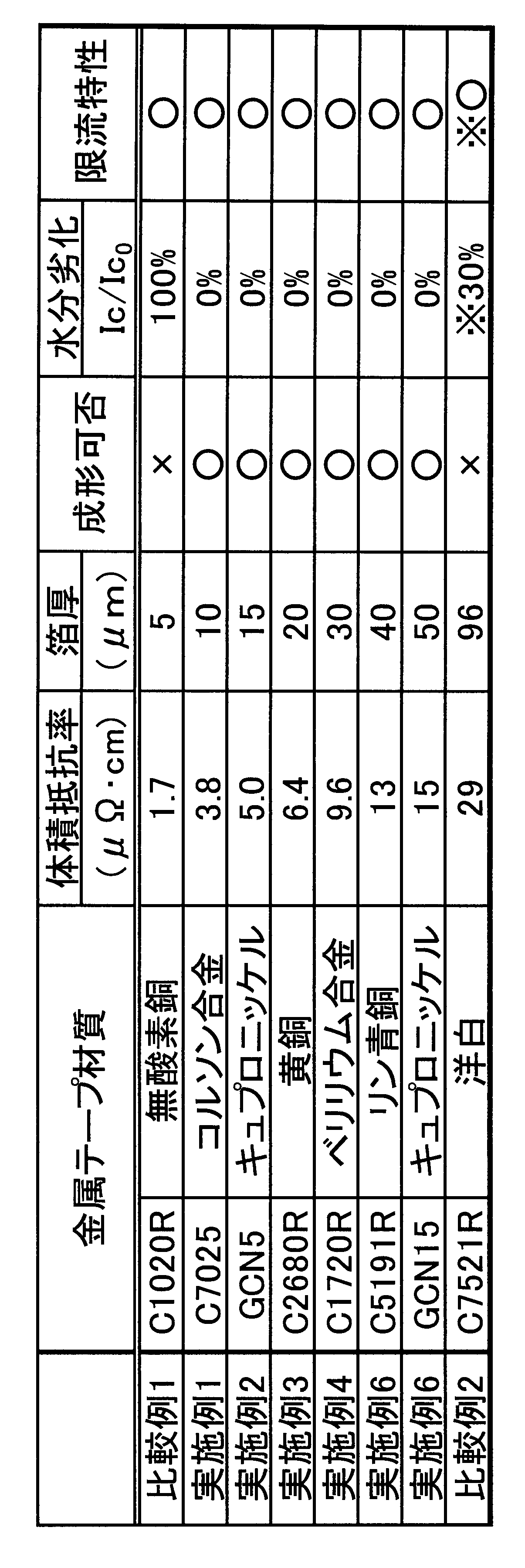
また、比較例2においては、金属テープとして使用した洋白は剛性が高くまた、箔厚が96μmと厚いため、洋白からなる金属テープをC字形に成形することができなかった。
そこで、比較例1、2の水分劣化及び限流特性に関しては、酸化物超電導積層体の保護層上に、表3に記載の箔厚の2倍の厚みを有する金属テープを、半田層を介して形成した線材について測定を行った。
比較例1、2の酸化物超電導線材は、酸化物超電導積層体を気密に被覆することができなかったため、プレッシャークッカー試験によって劣化した。
また、実施例1~6及び比較例1、2の酸化物超電導線材は、全て良好な限流特性を示した。一例として、実施例2の線材について観察された電流波形を示す図8を参照すると、第1波から徐々に電流値が抑制されていることがわかる。
以上のように、本発明の実施例に係る酸化物超電導線材は、良好な限流特性を示すことが確認された。さらに、本発明の実施例に係る酸化物超電導線材では、酸化物超電導積層体の周囲が所定の厚さの金属テープにより被覆されているため、過酷な状況においても水分による劣化が起こらないことが確認された。
2 金属テープ
3 基材
4 中間層
5 酸化物超電導層
6 保護層
7、17 半田層(低融点金属層)
10 安定化層
99 超電導限流器
A、B、C 酸化物超電導線材
D 膜厚(保護層)
d 厚さ(安定化層)
Claims (7)
- テープ状の基材と、前記基材上に積層された中間層と、前記中間層上に積層された酸化物超電導層と、前記酸化物超電導層上に積層されAg又はAg合金からなる保護層と、を有する酸化物超電導積層体と、
前記超電導積層体の保護層上に低融点金属層を介して形成され、金属テープからなる安定化層と、
を備える酸化物超電導線材であって、
前記保護層の膜厚が5μm以下であり、
前記安定化層の室温での体積抵抗率が3.8μΩ・cm以上15μΩ・cm以下である酸化物超電導線材。 - テープ状の基材と、前記基材上に積層された中間層と、前記中間層上に積層された酸化物超電導層と、前記酸化物超電導層に積層されAg又はAg合金からなる保護層と、を有する酸化物超電導積層体と、
前記超電導積層体の保護層上に低融点金属層を介して形成され、金属テープからなる安定化層と、
を備える酸化物超電導線材であって、
前記保護層の膜厚が5μm以下であり、
前記酸化物超電導線材の1cm幅、1cm長さにおける室温での抵抗値が150μΩ以上100mΩ以下である酸化物超電導線材。 - 前記安定化層を構成する前記金属テープの幅が、前記酸化物超電導積層体の幅よりも広く、
前記酸化物超電導積層体の保護層の上面と、前記保護層、前記酸化物超電導層、前記中間層及び前記基材の側面と、前記基材の裏面の少なくとも一部とが前記低融点金属層を介して前記安定化層により覆われている請求項1又は2に記載の酸化物超電導線材。 - 前記安定化層の厚みが9μm以上60μm以下である請求項3に記載の酸化物超電導線材。
- 請求項1から4の何れか一項に記載の酸化物超電導線材を備える超電導コイル。
- 請求項1から4の何れか一項に記載の酸化物超電導線材を備える超電導限流器。
- 請求項1から4の何れか一項に記載の酸化物超電導線材を備える超電導機器。
Priority Applications (4)
| Application Number | Priority Date | Filing Date | Title |
|---|---|---|---|
| US14/649,991 US20150318083A1 (en) | 2012-12-28 | 2013-12-26 | Oxide superconductor wire |
| RU2015126603/07A RU2597211C1 (ru) | 2012-12-28 | 2013-12-26 | Провод из оксидного сверхпроводника |
| JP2014538942A JP5693798B2 (ja) | 2012-12-28 | 2013-12-26 | 酸化物超電導線材 |
| EP13868560.7A EP2940699B1 (en) | 2012-12-28 | 2013-12-26 | Oxide superconductor wire |
Applications Claiming Priority (2)
| Application Number | Priority Date | Filing Date | Title |
|---|---|---|---|
| JP2012288302 | 2012-12-28 | ||
| JP2012-288302 | 2012-12-28 |
Publications (1)
| Publication Number | Publication Date |
|---|---|
| WO2014104208A1 true WO2014104208A1 (ja) | 2014-07-03 |
Family
ID=51021282
Family Applications (1)
| Application Number | Title | Priority Date | Filing Date |
|---|---|---|---|
| PCT/JP2013/084934 Ceased WO2014104208A1 (ja) | 2012-12-28 | 2013-12-26 | 酸化物超電導線材 |
Country Status (5)
| Country | Link |
|---|---|
| US (1) | US20150318083A1 (ja) |
| EP (1) | EP2940699B1 (ja) |
| JP (1) | JP5693798B2 (ja) |
| RU (1) | RU2597211C1 (ja) |
| WO (1) | WO2014104208A1 (ja) |
Cited By (1)
| Publication number | Priority date | Publication date | Assignee | Title |
|---|---|---|---|---|
| JP2016115574A (ja) * | 2014-12-16 | 2016-06-23 | 株式会社フジクラ | 超電導線材及びこれを使用した超電導コイル |
Families Citing this family (3)
| Publication number | Priority date | Publication date | Assignee | Title |
|---|---|---|---|---|
| JP2017117772A (ja) * | 2015-12-18 | 2017-06-29 | 株式会社フジクラ | 酸化物超電導線材の製造方法及び超電導コイルの製造方法 |
| WO2022158413A1 (ja) * | 2021-01-25 | 2022-07-28 | 国立研究開発法人産業技術総合研究所 | 高温超電導線材、およびその製造方法 |
| EP4246602A1 (de) | 2022-03-14 | 2023-09-20 | Theva Dünnschichttechnik GmbH | Hermetisch dichter hochtemperatursupraleitender bandleiter |
Citations (5)
| Publication number | Priority date | Publication date | Assignee | Title |
|---|---|---|---|---|
| JP2009022118A (ja) * | 2007-07-12 | 2009-01-29 | Jtekt Corp | モータ制御装置 |
| JP2010207059A (ja) * | 2009-03-06 | 2010-09-16 | Denso Corp | 電力変換装置 |
| WO2012039444A1 (ja) * | 2010-09-24 | 2012-03-29 | 株式会社フジクラ | 酸化物超電導線材およびその製造方法 |
| JP2012109254A (ja) * | 2011-12-27 | 2012-06-07 | Toshiba Corp | 超電導電流リード |
| JP2012169237A (ja) | 2011-01-25 | 2012-09-06 | Fujikura Ltd | 酸化物超電導線材およびその製造方法 |
Family Cites Families (15)
| Publication number | Priority date | Publication date | Assignee | Title |
|---|---|---|---|---|
| US3964934A (en) * | 1975-05-15 | 1976-06-22 | The Gates Rubber Company | High discharge capability sealed through connector |
| JPH07169343A (ja) * | 1993-10-21 | 1995-07-04 | Sumitomo Electric Ind Ltd | 超電導ケーブル導体 |
| US5851911A (en) * | 1996-03-07 | 1998-12-22 | Micron Technology, Inc. | Mask repattern process |
| JP2954124B2 (ja) * | 1998-01-07 | 1999-09-27 | 株式会社東芝 | 超電導限流素子 |
| US20040266628A1 (en) * | 2003-06-27 | 2004-12-30 | Superpower, Inc. | Novel superconducting articles, and methods for forming and using same |
| US7463915B2 (en) * | 2004-08-20 | 2008-12-09 | American Superconductor Corporation | Stacked filamentary coated superconductors |
| US7816303B2 (en) * | 2004-10-01 | 2010-10-19 | American Superconductor Corporation | Architecture for high temperature superconductor wire |
| US7674751B2 (en) * | 2006-01-10 | 2010-03-09 | American Superconductor Corporation | Fabrication of sealed high temperature superconductor wires |
| DE102006018492A1 (de) * | 2006-04-19 | 2007-10-25 | Tesa Ag | Blasenfrei verklebende Klebeschichten |
| WO2008118127A1 (en) * | 2006-07-21 | 2008-10-02 | American Superconductor Corporation | Low resistance splice for high temperature superconductor wires |
| US20080194411A1 (en) * | 2007-02-09 | 2008-08-14 | Folts Douglas C | HTS Wire |
| US8524067B2 (en) * | 2007-07-27 | 2013-09-03 | Nanotek Instruments, Inc. | Electrochemical method of producing nano-scaled graphene platelets |
| US20100019776A1 (en) * | 2008-07-23 | 2010-01-28 | Folts Douglas C | Method for analyzing superconducting wire |
| JP2012150914A (ja) * | 2011-01-17 | 2012-08-09 | Fujikura Ltd | 高抵抗材複合酸化物超電導線材 |
| EP2490272B1 (en) * | 2011-02-18 | 2013-08-21 | Bruker HTS GmbH | Superconducting element with elongated opening and method for manufacturing the same |
-
2013
- 2013-12-26 WO PCT/JP2013/084934 patent/WO2014104208A1/ja not_active Ceased
- 2013-12-26 EP EP13868560.7A patent/EP2940699B1/en not_active Not-in-force
- 2013-12-26 JP JP2014538942A patent/JP5693798B2/ja not_active Expired - Fee Related
- 2013-12-26 US US14/649,991 patent/US20150318083A1/en not_active Abandoned
- 2013-12-26 RU RU2015126603/07A patent/RU2597211C1/ru not_active IP Right Cessation
Patent Citations (5)
| Publication number | Priority date | Publication date | Assignee | Title |
|---|---|---|---|---|
| JP2009022118A (ja) * | 2007-07-12 | 2009-01-29 | Jtekt Corp | モータ制御装置 |
| JP2010207059A (ja) * | 2009-03-06 | 2010-09-16 | Denso Corp | 電力変換装置 |
| WO2012039444A1 (ja) * | 2010-09-24 | 2012-03-29 | 株式会社フジクラ | 酸化物超電導線材およびその製造方法 |
| JP2012169237A (ja) | 2011-01-25 | 2012-09-06 | Fujikura Ltd | 酸化物超電導線材およびその製造方法 |
| JP2012109254A (ja) * | 2011-12-27 | 2012-06-07 | Toshiba Corp | 超電導電流リード |
Non-Patent Citations (1)
| Title |
|---|
| See also references of EP2940699A4 |
Cited By (1)
| Publication number | Priority date | Publication date | Assignee | Title |
|---|---|---|---|---|
| JP2016115574A (ja) * | 2014-12-16 | 2016-06-23 | 株式会社フジクラ | 超電導線材及びこれを使用した超電導コイル |
Also Published As
| Publication number | Publication date |
|---|---|
| EP2940699A1 (en) | 2015-11-04 |
| EP2940699B1 (en) | 2018-12-05 |
| JP5693798B2 (ja) | 2015-04-01 |
| EP2940699A4 (en) | 2016-08-17 |
| US20150318083A1 (en) | 2015-11-05 |
| JPWO2014104208A1 (ja) | 2017-01-19 |
| RU2597211C1 (ru) | 2016-09-10 |
Similar Documents
| Publication | Publication Date | Title |
|---|---|---|
| EP2801983B1 (en) | Superconducting wire and superconducting coil | |
| US10128025B2 (en) | Oxide superconducting wire, superconducting device, and method for producing oxide superconducting wire | |
| CN103959401B (zh) | 氧化物超导电线材及其制造方法、超导电线圈和超导电缆 | |
| JP5841862B2 (ja) | 高温超電導線材および高温超電導コイル | |
| EP2958115B1 (en) | Oxide superconducting wire | |
| WO2011129252A1 (ja) | 超電導線材の電極部接合構造、超電導線材、及び超電導コイル | |
| JP5693798B2 (ja) | 酸化物超電導線材 | |
| JP2014130730A (ja) | 酸化物超電導線材の接続構造体及び接続方法並びに接続構造体を用いた酸化物超電導線材 | |
| JP6101490B2 (ja) | 酸化物超電導線材の接続構造体及び超電導機器 | |
| JP6101491B2 (ja) | 酸化物超電導線材及びその製造方法 | |
| JP2014143840A (ja) | テープ状超電導線材の端末構造体及びテープ状超電導線材の端末構造体の製造方法 | |
| JP2014154320A (ja) | 酸化物超電導線材の接続構造体及び超電導機器 | |
| JP6329736B2 (ja) | 積層パンケーキ型超電導コイル及びそれを備えた超電導機器 | |
| JP6069269B2 (ja) | 酸化物超電導線材、超電導機器及び酸化物超電導線材の製造方法 | |
| JP6002602B2 (ja) | 酸化物超電導線材の接続構造体及びその製造方法 | |
| JP2013225399A (ja) | 酸化物超電導線材および超電導コイル | |
| JP2014107149A (ja) | 酸化物超電導線材並びに当該酸化物超電導線材の接続構造体 | |
| JPWO2014104333A1 (ja) | 酸化物超電導線材の接続構造体およびその製造方法と超電導機器 | |
| US20180114638A1 (en) | Method of manufacturing oxide superconducting wire and method of manufacturing superconducting coil | |
| JP6461776B2 (ja) | 超電導線材および超電導線材の製造方法 | |
| JP7667034B2 (ja) | 超電導コイル | |
| JP5775810B2 (ja) | 酸化物超電導線材の製造方法 | |
| JP2014167847A (ja) | 酸化物超電導線材及び超電導コイル並びに酸化物超電導線材の製造方法 | |
| JP6484658B2 (ja) | 酸化物超電導線材及び超電導コイル | |
| JP2014022228A (ja) | 酸化物超電導導体および酸化物超電導導体の製造方法並びにそれを用いた超電導機器 |
Legal Events
| Date | Code | Title | Description |
|---|---|---|---|
| ENP | Entry into the national phase |
Ref document number: 2014538942 Country of ref document: JP Kind code of ref document: A |
|
| 121 | Ep: the epo has been informed by wipo that ep was designated in this application |
Ref document number: 13868560 Country of ref document: EP Kind code of ref document: A1 |
|
| WWE | Wipo information: entry into national phase |
Ref document number: 14649991 Country of ref document: US |
|
| WWE | Wipo information: entry into national phase |
Ref document number: 2013868560 Country of ref document: EP |
|
| NENP | Non-entry into the national phase |
Ref country code: DE |
|
| ENP | Entry into the national phase |
Ref document number: 2015126603 Country of ref document: RU Kind code of ref document: A |