WO2014106891A1 - Dispositif de communication sans fil et dispositif électronique - Google Patents
Dispositif de communication sans fil et dispositif électronique Download PDFInfo
- Publication number
- WO2014106891A1 WO2014106891A1 PCT/JP2013/050010 JP2013050010W WO2014106891A1 WO 2014106891 A1 WO2014106891 A1 WO 2014106891A1 JP 2013050010 W JP2013050010 W JP 2013050010W WO 2014106891 A1 WO2014106891 A1 WO 2014106891A1
- Authority
- WO
- WIPO (PCT)
- Prior art keywords
- resonator
- housing
- substrate
- wireless communication
- resonance
- Prior art date
- Legal status (The legal status is an assumption and is not a legal conclusion. Google has not performed a legal analysis and makes no representation as to the accuracy of the status listed.)
- Ceased
Links
Images


Classifications
-
- H—ELECTRICITY
- H01—ELECTRIC ELEMENTS
- H01Q—ANTENNAS, i.e. RADIO AERIALS
- H01Q1/00—Details of, or arrangements associated with, antennas
- H01Q1/12—Supports; Mounting means
- H01Q1/22—Supports; Mounting means by structural association with other equipment or articles
- H01Q1/24—Supports; Mounting means by structural association with other equipment or articles with receiving set
- H01Q1/241—Supports; Mounting means by structural association with other equipment or articles with receiving set used in mobile communications, e.g. GSM
- H01Q1/242—Supports; Mounting means by structural association with other equipment or articles with receiving set used in mobile communications, e.g. GSM specially adapted for hand-held use
- H01Q1/243—Supports; Mounting means by structural association with other equipment or articles with receiving set used in mobile communications, e.g. GSM specially adapted for hand-held use with built-in antennas
-
- H—ELECTRICITY
- H01—ELECTRIC ELEMENTS
- H01Q—ANTENNAS, i.e. RADIO AERIALS
- H01Q1/00—Details of, or arrangements associated with, antennas
- H01Q1/48—Earthing means; Earth screens; Counterpoises
-
- H—ELECTRICITY
- H01—ELECTRIC ELEMENTS
- H01Q—ANTENNAS, i.e. RADIO AERIALS
- H01Q13/00—Waveguide horns or mouths; Slot antennas; Leaky-waveguide antennas; Equivalent structures causing radiation along the transmission path of a guided wave
- H01Q13/10—Resonant slot antennas
- H01Q13/106—Microstrip slot antennas
-
- H—ELECTRICITY
- H01—ELECTRIC ELEMENTS
- H01Q—ANTENNAS, i.e. RADIO AERIALS
- H01Q7/00—Loop antennas with a substantially uniform current distribution around the loop and having a directional radiation pattern in a plane perpendicular to the plane of the loop
-
- H—ELECTRICITY
- H01—ELECTRIC ELEMENTS
- H01Q—ANTENNAS, i.e. RADIO AERIALS
- H01Q9/00—Electrically-short antennas having dimensions not more than twice the operating wavelength and consisting of conductive active radiating elements
- H01Q9/04—Resonant antennas
- H01Q9/0407—Substantially flat resonant element parallel to ground plane, e.g. patch antenna
Definitions
- the present invention relates to a wireless communication device and an electronic device.
- AV Analog Visual
- a case case of an AV device provided with a first window frame for millimeter-wave communication, and the first window frame are attached to the first case.
- an AV device including a first window that passes a millimeter wave signal see, for example, Patent Document 1.
- This AV apparatus is provided in the housing case between the semiconductor chip with an antenna, which is located inside the first window and radiates a millimeter-wave signal, and between the first window and the semiconductor chip with an antenna. And a dielectric waveguide or a waveguide realized by a waveguide groove.
- the millimeter wave signal radiated from the semiconductor chip with antenna is radiated to the outside through the waveguide and the first window.
- the conventional AV device When performing conventional wireless communication with other AV devices, the conventional AV device radiates the millimeter wave signal radiated from the semiconductor chip with the antenna to the outside through the waveguide and the first window as described above. Therefore, the transmission efficiency of wireless communication was low.
- an object is to provide a wireless communication device and an electronic device with good transmission efficiency.
- a wireless communication apparatus includes a first housing having a first opening, a second housing that is disposed to face the first housing, and that is opened to face the first opening.
- a first resonance having a second housing having an opening and a first resonator, the first resonator being disposed inside the first housing such that the first resonator faces outward from the first opening.
- An apparatus and a second resonator, and the second resonator is disposed inside the second casing so as to face outward from the second opening and to face the first resonator.
- a second resonance device is disposed inside the second casing so as to face outward from the second opening and to face the first resonator.
- FIG. 1 is a cross-sectional view illustrating a wireless communication device 100 and an electronic device 500 according to a first embodiment.
- 3 is a diagram showing a cross section of a waveguide of a resonance device of radio communication apparatus 100 according to Embodiment 1.
- FIG. 3 is a diagram illustrating a resonance device 120A of the wireless communication device 100 according to the first embodiment.
- FIG. It is a figure which shows the variation of the plane pattern of the 1st surface and the 2nd surface of 120 A of resonance apparatuses.
- 6 is a diagram illustrating a resonance device 120A1 of a wireless communication device 100 according to a modification of the first embodiment.
- FIG. 3 is a diagram illustrating a structure of a substrate 140A1 of the wireless communication device 100 according to Embodiment 1.
- FIG. 3 is a diagram illustrating a structure of a substrate 140A2 of the wireless communication device 100 according to the first embodiment.
- FIG. 3 is a diagram illustrating a structure of a substrate 140A3 of the wireless communication device 100 according to the first embodiment.
- FIG. 3 is a diagram illustrating a structure of a substrate 140A4 of the wireless communication device 100 according to the first embodiment.
- FIG. 3 is a diagram illustrating a structure of a substrate 140A1 of the wireless communication device 100 according to Embodiment 1.
- FIG. 3 is a diagram illustrating a structure of a substrate 140A2 of the wireless communication device 100 according to the first embodiment.
- FIG. 3 is a diagram illustrating a structure of a substrate 140A3 of the wireless communication device 100 according to the first embodiment.
- FIG. 3 is a diagram illustrating a structure of a substrate 140A4 of the
- FIG. 3 is a diagram illustrating a structure of a substrate 140A4 of the wireless communication device 100 according to the first embodiment.
- FIG. It is a figure which shows the cross-section of the radio
- 6 is a diagram showing a wireless communication device 100 according to a modification of the first embodiment.
- FIG. 6 is a cross-sectional view showing a wireless communication device 200 and an electronic device 520 according to Embodiment 2.
- FIG. 6 is a plan view showing a resonator 121A and an attenuation unit 210A of a resonance device 220A of a wireless communication device 200A of Embodiment 2.
- FIG. 6 is a plan view illustrating an exemplary configuration of an attenuation unit 210A of a wireless communication device 200A according to Embodiment 2.
- FIG. 6 is a cross-sectional view showing a wireless communication device 300 and an electronic device 530 according to Embodiment 3.
- FIG. 10 shows a wireless communication apparatus 300 according to a modification of the third embodiment.
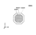
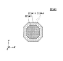
- 6 is a diagram illustrating a resonance device 320A of a wireless communication device 300 according to Embodiment 3.
- FIG. 6 is a diagram illustrating a resonance device 320A of a wireless communication device 300 according to Embodiment 3.
- FIG. 6 is a diagram illustrating a resonance device 320A of a wireless communication device 300 according to Embodiment 3.
- FIG. 6 is a diagram illustrating a resonance device 320A of a wireless communication device 300 according to Embodiment 3.
- FIG. 6 is a diagram illustrating a resonance device 320A of a wireless communication device 300 according to Embodiment 3.
- FIG. 1 is a cross-sectional view illustrating a wireless communication device 100 and an electronic device 500 according to the first embodiment.
- FIG. 2 is a diagram illustrating a cross section of the waveguide of the resonance device of the wireless communication device 100 according to the first embodiment.
- the wireless communication device 100 includes wireless communication devices 100A and 100B.
- the wireless communication device 100A includes a housing 110A and a resonance device 120A.
- the wireless communication device 100B includes a housing 110B and a resonance device 120B.
- the electronic device 500 of the first embodiment includes an electronic device 500A and an electronic device 500B.
- the electronic device 500A includes a wireless communication device 100A, a substrate 130A, a substrate 140A, and a circuit device 150A.
- the electronic device 500B includes a wireless communication device 100B, a substrate 130B, a substrate 140B, and a circuit device 150B.
- substrate 140A are handled as a component of the electronic apparatus 500A here, the board
- the substrate 130B and the substrate 140B are handled as components of the electronic device 500B, but the substrate 130B and the substrate 140B may be handled as components of the wireless communication device 100B. That is, the wireless communication device 100B may be handled as including the housing 110B, the resonance device 120B, the substrate 130B, and the substrate 140B.
- the housings 110A and 110B are, for example, metal housings, and have wall portions 110A1 and 110B1, respectively.
- the casings 110A and 110B are arranged side by side with the wall portions 110A1 and 110B1 being close to each other and substantially parallel to each other.
- the housing 110A is an example of a first housing, and the housing 110B is an example of a second housing.
- the wall portion 110A1 is an example of a first wall portion, and the wall portion 110B1 is an example of a second wall portion.
- the housings 110A and 110B have openings 110A2 and 110B2 formed in the walls 110A1 and 110B1, respectively.
- the opening 110A2 is an example of a first opening
- the opening 110B2 is an example of a second opening.
- FIG. 1 shows a state in which the waveguides 122A and 122B of the resonance devices 120A and 120B are fitted in the openings 110A2 and 110B2, respectively.
- the openings 110A2 and 110B2 are rectangular openings in a plan view that matches the cross-sectional shape of the waveguides 122A and 122B.
- FIG. 1 shows only the wall 110A1 in which the opening 110A2 is formed among the walls of the housing 110A.
- the housing 110A includes the resonance device 120A, the substrates 130A and 140A, and the circuit device 150A. It is formed so as to surround (incorporate).
- FIG. 1 shows only the wall 110B1 in which the opening 110B2 is formed among the walls of the housing 110B.
- the housing 110B includes the resonance device 120B, the substrates 130B and 140B, and the circuit device 150B. Is formed so as to surround (internally).
- the resonance devices 120A and 120B are fitted in the openings 110A2 and 110B2, respectively.
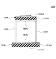
- the resonance device 120A includes a resonance substrate 121A, a waveguide 122A, and a resonance substrate 123A.
- the resonance device 120B includes a resonance substrate 121B, a waveguide 122B, and a resonance substrate 123B.
- the resonance device 120A is an example of a first resonance device
- the resonance device 120B is an example of a second resonance device.
- the waveguide 122A is an example of a first waveguide
- the waveguide 122B is an example of a second waveguide.
- the resonance device 120A is fitted into the opening 110A2 so that the resonator 121A1 of the resonance substrate 121A faces the outside of the housing 110A from the opening 110A2. Since the waveguide 122A of the resonance device 120A has a rectangular cross section, the opening 110A2 is opened in a rectangular shape in accordance with the cross-sectional shape of the waveguide 122A.
- the resonator 121A1 is an example of a first resonator.
- the radiation surface of the resonator 121A1 is located outside the housing 110A rather than the surface located inside the housing 110A of the wall 110A1. That is, the resonator 121A1 is disposed so that the radiation surface is located outside the housing 110A with respect to the inner wall surface 110A11 of the housing 110A.
- the resonance device 120B is fitted into the opening 110B2 so that the resonator 121B1 of the resonance substrate 121B faces the outside of the housing 110B from the opening 110B2. Since the waveguide 122B of the resonance device 120B has a rectangular cross section, the opening 110B2 is opened in a rectangular shape in accordance with the cross-sectional shape of the waveguide 122B.
- the resonator 121B1 is an example of a second resonator.
- the radiation surface of the resonator 121B1 is located outside the housing 110B rather than the surface located inside the housing 110B of the wall portion 110B1.
- the resonator 121B1 is disposed so that the radiation surface is positioned outside the housing 110B with respect to the inner wall surface 110B11 of the housing 110B1.
- the resonant substrate 121A includes a resonator 121A1, a resonator 121A2, and an insulating layer 121A3.
- the resonator 121A1 is formed on the surface of the insulating layer 121A3 opposite to the surface connected to the waveguide 122A, and the resonator 121A2 is formed on the surface of the insulating layer 121A3 connected to the waveguide 122A.
- the resonators 121A1 and 121A2 are formed, for example, by patterning a copper foil attached to the front and back surfaces of the insulating layer 121A3.
- the resonant substrate 121A transmits electromagnetic waves between the resonators 121A1 and 121A2.
- the resonant substrate 121B includes a resonator 121B1, a resonator 121B2, and an insulating layer 121B3.
- the resonator 121B1 is formed on the surface of the insulating layer 121B3 opposite to the surface connected to the waveguide 122B, and the resonator 121B2 is formed on the surface connected to the waveguide 122B of the insulating layer 121B3.
- the resonators 121B1 and 121B2 are formed, for example, by patterning a copper foil attached to the front and back surfaces of the insulating layer 121B3.
- the resonant substrate 121B transmits electromagnetic waves between the resonators 121B1 and 121B2.
- the waveguides 122A and 122B are constructed of, for example, a metal film molded into a rectangular tube having a cross section as shown in FIG. Or, for example, as shown in FIGS. 2 (B), (C), (D), and (E), the waveguide has an octagonal shape in which the four corners of the outside or inside of the rectangular tube are deformed to 45 degrees obliquely. It is also possible to use a rectangular tube whose outer or inner four corners are deformed into an arc shape. Such a rounded shape makes it easier to form or fit into the housing opening.
- the metal film for example, a copper foil or a metal foil made of aluminum can be used.
- a metal layer may be formed on the inner surface of a rectangular tubular or deformed rectangular resin member.
- a hollow waveguide shape having only a metal layer without an internal resin may be used.
- the metal layer may be a metal layer made of copper or aluminum, for example.
- the waveguide 122A is connected to the metal layers of the resonator 121A2 and the resonator 123A2, and is held at the same potential as the metal layers of the resonator 121A2 and the resonator 123A2.
- the waveguide 122B is connected to the metal layers of the resonator 121B2 and the resonator 123B2, and is held at the same potential as the metal layers of the resonator 121B2 and the resonator 123B2.
- the detailed configuration will be described later with reference to FIG.
- One end (the lower end in FIG. 1) of the waveguide 122A is connected to the resonator 121A2 of the resonance substrate 121A, and the other end (the upper terminal in FIG. 1) is the resonance of the resonance substrate 123A. Connected to the device 123A2.
- the waveguide 122A forms a waveguide between the resonator 121A2 and the resonator 123A2.
- the cross section of the waveguide 122A parallel to the resonance substrates 121A and 123A is rectangular.
- the waveguide 122A transmits electromagnetic waves between the resonant substrates 121A and 123A.
- one end (the upper end in FIG. 1) of the waveguide 122B is connected to the resonator 121B2 of the resonant substrate 121B, and the other end (the lower terminal in FIG. 1) is connected to the resonant substrate. It is connected to the 123B resonator 123B2.
- the waveguide 122B forms a waveguide between the resonator 121B2 and the resonator 123B2.
- the cross section of the waveguide 122B parallel to the resonance substrates 121B and 123B is rectangular.
- the waveguide 122B transmits electromagnetic waves between the resonant substrates 121B and 123B.
- the resonant substrate 123A includes a resonator 123A1, a resonator 123A2, and an insulating layer 123A3.
- the resonator 123A1 is formed on the surface of the insulating layer 123A3 opposite to the surface connected to the waveguide 122A, and the resonator 123A2 is formed on the surface of the insulating layer 123A3 connected to the waveguide 122A.
- the resonator 123A1 is an example of a third resonator.
- the resonators 123A1 and 123A2 are formed, for example, by patterning a copper foil attached to the front and back surfaces of the insulating layer 123A3.
- the resonant substrate 123A transmits electromagnetic waves between the resonators 123A1 and 123A2.
- the resonator 123A1 transmits electromagnetic waves to and from the resonator 141A of the substrate 140A.
- the resonant substrate 123B includes a resonator 123B1, a resonator 123B2, and an insulating layer 123B3.
- the resonator 123B1 is formed on the surface of the insulating layer 123B3 opposite to the surface connected to the waveguide 122B, and the resonator 123B2 is formed on the surface of the insulating layer 123B3 connected to the waveguide 122B.
- the resonator 123B1 is an example of a fourth resonator.
- the resonators 123B1 and 123B2 are formed, for example, by patterning a copper foil attached to the front and back surfaces of the insulating layer 123B3.
- the resonant substrate 123B transmits electromagnetic waves between the resonators 123B1 and 123B2.
- the resonator 123B1 transmits electromagnetic waves between the resonator 141B of the substrate 140B.
- the substrates 130A and 130B are disposed inside the housings 110A and 110B, respectively, and the substrates 140A and 140B are mounted thereon.
- the boards 130A and 130B are larger than the boards 140A and 140B, for example, printed boards (PCB: Printed Circuit Circuit Board) according to the FR-4 (Flame Retardant Type 4) standard, etc. It includes a plurality of wiring layers disposed on the back surface.
- the boards 140A and 140B are mounted on the boards 130A and 130B in the housings 110A and 110B, respectively.
- the boards 140A and 140B are printed boards conforming to the FR-4 standard, for example.
- the substrate 140A includes a resonator 141A, wiring layers 142A and 143A, and an insulating layer 144A.
- the resonator 141A and the wiring layers 142A and 143A are formed by patterning a copper foil attached to the front surface and the back surface of the insulating layer 144A.
- the resonator 141A transmits electromagnetic waves to and from the resonator 123A1 of the resonance substrate 123A.
- the wiring layers 142A and 143A are held at the ground potential.
- a circuit device 150A is mounted on the wiring layer 142A via solder balls 151A.
- the substrate 140A is connected to the substrate 130A via the wiring layer 143A.
- the substrate 140B includes a resonator 141B, wiring layers 142B and 143B, and an insulating layer 144B.
- the resonator 141B and the wiring layers 142B and 143B are formed by patterning a copper foil attached to the front surface and the back surface of the insulating layer 144B.
- the resonator 141B transmits electromagnetic waves to and from the resonator 123B1 of the resonance substrate 123B.
- the wiring layers 142B and 143B are held at the ground potential.
- the circuit device 150B is mounted on the wiring layer 142B via the solder balls 151B.
- the substrate 140B is connected to the substrate 130B through the wiring layer 143B.
- the circuit devices 150A and 150B are flip-chip mounted on the substrates 140A and 140B by being connected to the substrates 140A and 140B via the solder balls 151A and 151B and being fixed by the underfill materials 152A and 152B, respectively.
- the circuit devices 150A and 150B are connected to the resonators 141A and 141B via the transmission paths of the substrates 140A and 140B, respectively.
- the circuit devices 150A and 150B are, for example, a transceiver for wireless communication, a transceiver such as a video signal, or an arithmetic processing device that performs predetermined arithmetic processing, and the signals radiated from the resonance devices 120A and 120B, respectively. Output.
- signals can be transmitted and received between the resonator 121A1 of the wireless communication device 100A and the circuit device 150A of the electronic device 500A including the wireless communication device 100A.
- signals can be transmitted and received between the resonator 121B1 of the wireless communication device 100B and the circuit device 150B of the electronic device 500B including the wireless communication device 100B.
- the circuit device 150A and Signals can be transmitted to and received from 150B.
- the resonance device 120A included in the wireless communication device 100 of the first embodiment will be described with reference to FIG. 3 and FIG. Since the resonance devices 120A and 120B shown in FIG. 1 have the same configuration, the resonance device 120A will be described here.
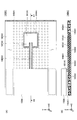
- FIG. 3 is a diagram illustrating the resonance device 120A of the wireless communication device 100 according to the first embodiment.
- FIG. 4 is a diagram showing variations of the planar pattern of the first surface and the second surface of the resonance device 120A.
- the resonance device 120A shown in FIG. 3 is the same as the resonance device 120A shown in FIG.
- the resonance device 120A includes a resonance substrate 121A, a waveguide 122A, and a resonance substrate 123A.
- the first surface is a surface opposite to the surface to which the waveguide 122A of the resonance substrate 121A is connected, and a surface opposite to the surface to which the waveguide 122A of the resonance substrate 123A is connected.
- the resonator 121A1 is formed on the first surface
- the resonator 123A1 is formed on the first surface.
- the second surface represents a surface to which the waveguide 122A of the resonance substrate 121A is connected and a surface to which the waveguide 122A of the resonance substrate 123A is connected. That is, in the resonant substrate 121A shown in FIG. 3, the resonator 121A2 is formed on the second surface, and in the resonant substrate 123A shown in FIG. 3, the resonator 123A2 is formed on the second surface. Become.
- 4A to 4E show variations of the planar patterns of the first and second surfaces of the resonant substrates 121A and 123A.
- the insulating layer 180C shown in FIGS. 4A to 4E corresponds to the insulating layer 121A3 of the resonant substrate 121A or the insulating layer 123A3 of the resonant substrate 123A.
- the first surface shown in the upper stage represents a planar pattern of the first surfaces of the resonance substrates 121A and 123A
- the second surface shown in the lower stage represents the first surfaces of the resonance substrates 121A and 123A. Represents a single plane pattern.
- FIGS. 4A to 4E the metal film is shown in white and the insulator is shown in gray.
- the first surface may be provided with a resonator in which a rectangular metal patch 180A in a plan view is formed on one surface of an octagonal insulating layer 180C in a plan view.
- the second surface may be a resonator in which a pair of slots 180B are formed in a metal layer 180D formed on the entire other surface of the insulating layer 180C.
- the slot 180B on the second surface is a pair of elongated holes formed in the metal layer 180D formed on the entire surface of the insulating layer 180C, and is a portion where the metal layer 180D is not formed.
- the interval between the pair of slots 180B is set to a half length ( ⁇ / 2) of the wavelength ⁇ at the communication frequency.
- the length of the slot 180B in the longitudinal direction is preferably different from the half length ( ⁇ / 2) of the wavelength ⁇ at the communication frequency.
- the width of each of the pair of slots 180B may be set to an appropriate width according to the radiation characteristics of the resonators 121A2 and 123A2.
- the length of the side in the vertical direction of the metal patch 180A on the first surface in the drawing may be set to a length ( ⁇ / 2) that is half the wavelength ⁇ at the communication frequency, for example.
- the length of the side in the vertical direction of the metal patch 180A on the first surface in the drawing is a length corresponding to the interval between the slots 180B on the second surface.
- the length of the side in the figure of the metal patch 180A on the first surface may be different from the half length ( ⁇ / 2) of the wavelength ⁇ at the communication frequency.
- center point of the metal patch 180A in plan view and the center point of the pair of slots 180B in plan view coincide.
- the resonator 121A1 of the resonance substrate 121A or the resonator 123A1 of the resonance substrate 123A is a resonance in which the metal patch 180A is formed on the insulating layer 180C as shown in the first surface of FIG. It may be a vessel.
- the resonator 121A2 of the resonance substrate 121A or the resonator 123A2 of the resonance substrate 123A has a slot 180B in the metal layer 180D formed on the entire surface of the insulating layer 180C, as shown on the second surface of FIG. It may be a resonator in which is formed.
- the metal layer 180D may be handled as a ground element.
- one end (upper end in FIG. 1) and the other end (lower end in FIG. 1) of the waveguide 122A are both connected to the metal layer 180D.
- a metal layer may not be formed on the first surface.
- the first surface is covered with the insulating layer 180C, and there is no resonator on the first surface.
- the second surface may be a resonator in which a pair of slots 180B are formed in a metal layer 180D formed on the entire other surface of the insulating layer 180C, as in FIG.
- the insulating layer 180C may be formed on one surface as shown in the first surface of FIG.
- the first surface of the resonance substrate 123A may not be provided with the resonator 123A1, and the insulating layer 180C may be formed over the entire surface as shown in the first surface of FIG.
- the resonator 121A2 of the resonance substrate 121A or the resonator 123A2 of the resonance substrate 123A has a slot 180B in the metal layer 180D formed on the entire surface of the insulating layer 180C, as shown in the second surface of FIG. It may be a resonator in which is formed.
- one end (upper end in FIG. 1) and the other end (lower end in FIG. 1) of the waveguide 122A are both connected to the metal layer 180D.
- the resonance substrate 121A is separated from the resonance substrate 123A by the resonator 121A2 on the second surface. Electromagnetic waves will be transmitted.
- the resonance substrate 123A when there is no resonator on the first surface of the resonance substrate 123A, the resonance substrate 123A is separated from the resonance substrate 121A by the resonator 123A2 on the second surface. Will transmit electromagnetic waves.
- a metal layer may not be formed on the first surface.
- the first surface is covered with the insulating layer 180C as in FIG. 4B, and there is no resonator on the first surface.
- the second surface may be a resonator formed by surrounding the metal patch 180E formed on the other surface of the insulating layer 180C with a ground element 180F.
- the metal patch 180E on the second surface is a rectangular metal patch formed in the center of the other surface of the insulating layer 180C in plan view, and is the same as the metal patch 180A shown on the first surface in FIG. Has a shape.
- the ground element 180F is formed around the metal patch 180E on the other surface of the insulating layer 180C, and has an opening 180F1 concentric with the metal patch 180E.
- the ground element 180F may be held at a ground potential, a predetermined reference potential, or an arbitrary potential of a floating potential.
- the metal patch 180E on the second surface has, for example, one of the length of the side in the vertical direction in the figure and the length of the side in the horizontal direction in the figure is half the wavelength ⁇ at the communication frequency. What is necessary is just to set to ((lambda) / 2). In this case, the length of one of the other sides is preferably different from the half length ( ⁇ / 2) of the wavelength ⁇ at the communication frequency.
- center point of the metal patch 180E in plan view and the center point of the ground element 180F in plan view coincide with each other.
- the gap where the metal patch 180E on the second surface and the insulating layer 180C of the ground element 180F are visible is preferably equal to the slot width in FIG.
- the insulating layer 180C may be formed on one surface as shown in the first surface of FIG.
- the first surface of the resonance substrate 123A may not be provided with the resonator 123A1, and the insulating layer 180C may be formed over the entire surface as shown in the first surface of FIG.
- the resonator 121A2 of the resonant substrate 121A or the resonator 123A2 of the resonant substrate 123A has a metal patch 180E and a ground element on the other surface of the insulating layer 180C, as shown on the second surface of FIG.
- positioned by concentric rectangular shape may be sufficient.
- one end (upper end in FIG. 1) and the other end (lower end in FIG. 1) of the waveguide 122A are both connected to the ground element 180F.
- the resonance substrate 121A transmits electromagnetic waves to and from the resonance substrate 123A by the resonator 121A2 on the second surface. Will do.
- the resonance substrate 123A when there is no resonator on the first surface of the resonance substrate 123A, the resonance substrate 123A is separated from the resonance substrate 121A by the resonator 123A2 on the second surface. Electromagnetic waves will be transmitted.
- the first surface is provided with a resonator in which a pair of elongated rectangular metal patches 180G are formed on one surface of an octagonal insulating layer 180C in plan view. May be.
- the second surface may be a resonator in which a pair of slots 180B are formed in a metal layer 180D formed on the entire other surface of the insulating layer 180C.
- the pair of metal patches 180G on the first surface is formed in a direction 90 degrees different from the slot 180B on the second surface in plan view. That is, the pair of metal patches 180G and the slot 180B are formed to be orthogonal to each other in plan view.
- the length in the longitudinal direction of the pair of metal patches 180G may be set to a length ( ⁇ / 2) that is half the wavelength ⁇ at the communication frequency, for example.
- the width of each of the pair of metal patches 180G may be set to an appropriate width according to the radiation characteristics of the resonators 121A1 and 123A1.
- the slot 180B on the second surface is the same as the slot 180B shown in FIG.
- the resonator 121A1 of the resonance substrate 121A or the resonator 123A1 of the resonance substrate 123A forms a pair of metal patches 180G on the insulating layer 180C as shown in the first surface of FIG. It may be a resonator.
- the resonator 121A2 of the resonant substrate 121A or the resonator 123A2 of the resonant substrate 123A has a slot 180B in the metal layer 180D formed on the entire surface of the insulating layer 180C, as shown on the second surface of FIG. It may be a resonator in which is formed.
- one end (upper end in FIG. 1) and the other end (lower end in FIG. 1) of the waveguide 122A are both connected to the ground element 180F.
- a metal layer may not be formed on the first surface.
- the first surface is covered with the insulating layer 180C in the same manner as in FIGS. 4B and 4C.
- the second surface may be covered with the insulating layer 180C without forming a metal layer.
- the thickness of the insulating layer 180C may be set to a length ( ⁇ / 2) that is half the wavelength ⁇ at the communication frequency.
- the resonator 121A1 of the resonant substrate 121A or the resonator 123A1 of the resonant substrate 123A has a thickness that is half the wavelength ⁇ (see FIG. 4E).
- a resonator in which an insulating layer 180C set to ⁇ / 2) is formed on one surface may be used.
- the resonator 121A2 of the resonance substrate 121A or the resonator 123A2 of the resonance substrate 123A has a thickness ( ⁇ / 2) that is half the wavelength ⁇ , as shown on the second surface of FIG.
- a resonator in which the insulating layer 180C set in (1) is formed on one surface may be used.
- one end (upper end in FIG. 1) and the other end (lower end in FIG. 1) of the waveguide 122A are both connected to the insulating layer 180C.
- the plane patterns of the first surface and the second surface of the resonance substrates 121A and 123A of the resonance device 120A of the wireless communication device 100 according to the first embodiment are, for example, as shown in (A) to (E) of FIG. A plane pattern as shown can be obtained.
- the plane patterns of the first and second surfaces of the resonance substrates 121B and 123B of the resonance device 120B of the wireless communication apparatus 100 are the plane patterns of the first and second surfaces of the resonance substrates 121A and 123A of the resonance device 120A. The same can be done.
- the plane patterns of the first and second surfaces of the resonance substrates 121A and 123A of the resonance device 120A and the plane patterns of the first and second surfaces of the resonance substrates 121B and 123B may be different from each other. .
- the plane patterns of the first and second surfaces of the resonance substrates 121A and 123A of the resonance device 120A and the plane patterns of the first and second surfaces of the resonance substrates 121B and 123B are shown in FIG.
- the resonator is not limited to the pattern shown in (E), and may be a resonator having another pattern.
- first surface and the second surface of the resonance substrate 123A of the resonance device 120A shown in FIG. 3 can be changed, for example, by using vias as shown in FIG.
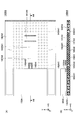
- FIG. 5 is a diagram illustrating a resonance device 120A1 of the wireless communication device 100 according to the modification of the first embodiment.
- FIG. 6 is a diagram showing variations of the planar pattern of the first surface and the second surface of the resonance substrate 123A of the resonance device 120A1 shown in FIG.
- the resonance device 120A1 shown in FIG. 5 includes a resonance substrate 121A, a waveguide 122A, and a resonance substrate 123A.
- the resonance substrate 121A and the waveguide 122A shown in FIG. 5 are the same as the resonance substrate 121A and the waveguide 122A of the resonance device 120A shown in FIG. 3, respectively.
- a resonant substrate 123A shown in FIG. 5 has a configuration in which a ground element 123A12 is added to the first surface of the resonant substrate 123A shown in FIG.
- the resonator 123A1 includes a metal patch 123A11 and a ground element 123A12 formed around the metal patch 123A11 in plan view.
- the resonator 123A2 includes a metal patch 123A21 and a ground element 123A22 formed around the metal patch 123A21 in plan view.
- the ground element 123A22 of the resonator 123A2 is connected to the ground element 123A12 of the resonator 123A1 by a via 123A4.
- the planar pattern of the first surface and the second surface of the resonant substrate 123A will be described with reference to FIG.
- the insulating layer 180C shown in FIGS. 6A to 6C corresponds to the insulating layer 123A3 of the resonant substrate 123A.
- the first surface shown in the upper part shows a planar pattern of the first surface of the resonance substrate 123A.
- the second surface shown in the lower stage shows a planar pattern of the second surface of the resonance substrate 123A.
- the metal film is shown in white and the insulator is shown in gray.
- the first surface has a rectangular metal patch 190A1 in a plan view, an octagonal annular ground element 190A2 in a plan view, and one of an octagonal insulating layer 190C in a plan view.
- a resonator formed on the surface may be provided.
- the second surface may be a resonator in which a pair of slots 190B are formed in a metal layer 190D formed on the entire other surface of the insulating layer 190C.
- ground element 190A2 on the first surface and the metal layer 190D on the second surface may be connected by the via 190G.
- the length of the vertical side in the drawing of the metal patch 190A1 on the first surface may be set to, for example, a length ( ⁇ / 2) half of the wavelength ⁇ at the communication frequency. This is the same as the metal patch 180A shown in FIG.
- the slot 190B on the second surface is a pair of elongated holes formed in the metal layer 190D formed on the entire surface of the insulating layer 190C, and is a portion where the metal layer 190D is not formed.
- the length, interval, and width of the slot 190B are the same as the length, interval, and width of the slot 180B shown in FIG.
- the resonator 123A1 of the resonance substrate 123A may be a resonator in which the metal patch 190A1 and the ground element 190A2 are formed on the insulating layer 190C as shown in the first surface of FIG. .
- the resonator 123A2 of the resonance substrate 123A may be a resonator in which a slot 190B is formed in a metal layer 190D formed on the entire surface of the insulating layer 190C, as shown on the second surface in FIG. .
- ground element 190A2 on the first surface and the metal layer 190D on the second surface may be connected by the via 190G.
- one end (the upper end in FIG. 1) of the waveguide 122A is connected to the metal layer 190D.
- the metal layer 190D may be handled as a ground element.
- the octagonal annular ground element 190A2 in the plan view may be formed on one surface of the octagonal insulating layer 190C in the plan view on the first surface.
- the planar pattern shown on the first surface in FIG. 6B is obtained by adding a ground element 190A2 to the planar pattern shown in FIG. For this reason, the resonator does not exist in the plane pattern shown on the first surface in FIG.
- the second surface may be a resonator in which a pair of slots 190B are formed in a metal layer 190D formed on the entire other surface of the insulating layer 190C.
- ground element 190A2 on the first surface and the metal layer 190D on the second surface may be connected by the via 190G.
- the resonator 123A1 may have a configuration in which the metal patch 190A1 is removed from the first surface shown in FIG.
- the ground element 190A2 is formed on the insulating layer 190C on the first surface of the resonance substrate 123A without providing the resonator 123A1, as shown in the first surface of FIG. 6B. Also good.
- the resonator 123A2 of the resonance substrate 123A is a resonator in which a slot 190B is formed in a metal layer 190D formed on the other surface of the insulating layer 190C, as shown on the second surface of FIG. 6B. There may be.
- the ground element 190A2 and the metal layer 190D may be connected by a via 190G.
- the via 190G corresponds to the via 123A4 illustrated in FIG.
- one end (the upper end in FIG. 1) of the waveguide 122A is connected to the metal layer 190D.
- the metal layer 190D may be handled as a ground element.
- the resonance substrate 123A when there is no resonator on the first surface of the resonance substrate 123A, the resonance substrate 123A is separated from the resonance substrate 121A by the resonator 123A2 on the second surface. Electromagnetic waves will be transmitted.
- the second surface may be a resonator formed by surrounding a metal patch 190E formed on the other surface of the insulating layer 190C with a ground element 190F. .
- the metal patch 190E on the second surface is a rectangular metal patch formed in the center of the other surface of the insulating layer 190C in a plan view, and is the same as the metal patch 180E shown on the second surface in FIG. Has a shape.
- the ground element 190F is formed around the metal patch 190E on the other surface of the insulating layer 190C, and has an opening 190F1 concentric with the metal patch 190E.
- the length of the side of the metal patch 190E on the second surface may be the same as the length of the side of the metal patch 180E shown in FIG.
- one end (the upper end in FIG. 1) of the waveguide 122A is connected to the ground element 190F.
- the first surface of the resonance substrate 123A is not provided with the resonator 123A1 and the ground element 190A2 is formed on the insulating layer 190C as shown in the first surface of FIG. Good.
- a metal patch 190E and a ground element 190F are concentrically arranged on the other surface of the insulating layer 190C.
- the resonator formed by this may be sufficient.
- the ground element 190A2 and the ground element 190F may be connected by the via 190G.
- the via 190G corresponds to the via 123A4 illustrated in FIG.
- the resonance substrate 123A when there is no resonator on the first surface of the resonance substrate 123A, the resonance substrate 123A is separated from the resonance substrate 121A by the resonator 123A2 on the second surface. Electromagnetic waves will be transmitted.
- the structure of the boards 140A and 140B of the wireless communication apparatus 100 according to the first embodiment will be described with reference to FIGS. Since the substrates 140A and 140B have the same configuration, the substrate 140A will be described here.
- FIGS. 7 to 11 are diagrams illustrating the structures of the substrates 140A1 to 140A4 of the wireless communication apparatus 100 according to the first embodiment.
- the substrate 140A shown in FIG. 1 may be any one of the substrates 140A1 to 140A4 shown in FIGS. 7 to 11, for example. 7 to 11, (A) is a plan view, and (B) is a view showing a cross section taken along arrows A1-A1 to A4-A4 in (A).
- solder ball 151 and the underfill material 152A are omitted for easy understanding of the structure. 7 to 11, an XYZ coordinate system that is an orthogonal coordinate system is defined as shown. 7 to 11, the metal film is shown in white and the insulator is shown in gray.
- the solder balls 151 may be metal bumps.
- the substrate 140A1 includes a resonator 141A1, wiring layers 142A1, 143A1, an insulating layer 144A1, a via 145A1, a coplanar line (Coplanar wave guide (CPW)) 146A1, and a connection path 147A1.
- CPW Coplanar wave guide
- the resonator 141A1 is a rectangular metal patch in plan view, and a coplanar line 146A1 is connected to the center of the side on the negative side in the X-axis via a connection path 147A1.
- the connection path 147A1 is a portion that penetrates into the metal patch of the rectangular resonator 141A1 in plan view.
- the connection path 147A1 is formed for impedance matching between the coplanar line 146A1 and the resonator 141A1.
- the resonator 141A1 is formed together with the coplanar line 146A1, the connection path 147A1, and the wiring layer 142A1, for example, by patterning a copper foil formed on the surface on the Z-axis positive direction side of the insulating layer 144A1.
- the wiring layer 142A1 is held at the ground potential and functions as a ground element.
- the wiring layer 142A1 surrounds the resonator 141A1 in a plan view on the surface on the Z-axis positive direction side of the insulating layer 144A1, and is formed along both sides of the coplanar line 146A1.
- the wiring layer 142A1 is also formed in a portion located below the circuit device 150A. That is, the wiring layer 142A1 is formed so as to cover substantially the entire surface excluding the resonator 141A1 and the coplanar line 146A1. The wiring layer 142A1 is connected to the wiring layer 143A1 through the via 145A1. The wiring layers 142A1 and 143A1 are held at the ground potential.
- the wiring layer 143A1 is formed on the entire surface of the insulating layer 144A1 on the Z axis negative direction side.
- the wiring layer 143A1 is connected to the wiring layer 142A1 by the via 145A1, and is held at the ground potential.
- the insulating layer 144A1 is, for example, an insulating layer in which glass fiber is impregnated with an epoxy resin when the substrate 140A1 is a printed circuit board conforming to the FR-4 standard.
- the inner wiring layer of the insulating layer 144A1 is not shown, an inner wiring layer may be formed in the insulating layer 144A1.
- the via 145A1 connects the wiring layers 142A1 and 143A1.
- a large number of vias 145A1 are formed so as to connect the wiring layers 142A1 and 143A1 over the whole in a plan view.
- the via 145A1 is formed around the rectangular resonator 141A1 in a plan view, on both sides of the coplanar line 146A1, on the lower side of the circuit device 150A, and so on.
- the mark 145 indicates that the via 145A1 is formed to the ends of the wiring layer 142A1 on the Y axis positive direction side and the Y axis negative direction side.
- the vias 145A1 are not formed in the regions indicated by the broken frame on the Y-axis positive direction side and the Y-axis negative direction side of the circuit device 150A because the terminals of the circuit device 150A are formed.
- the pitch of the vias 145A1 formed in this manner is set so that, for example, the interval between adjacent vias 145A1 is less than half of the wavelength ⁇ at the communication frequency of wireless communication, and more preferably ⁇ / 4 or less.
- the coplanar line 146A1 has an end on the X-axis positive direction side connected to the resonator 141A1, and an end on the X-axis negative direction side connected to a terminal of the circuit device 150A via the bump 151A1.
- the coplanar line 146A1 is an example of a first transmission line.
- the coplanar line formed on the substrate 140B similarly to the coplanar line 146A1 is an example of a second transmission line.
- the coplanar line 146A1 is a transmission line having a characteristic impedance of 50 ⁇ , and is provided to suppress a decrease in signal transmission efficiency between the resonator 141A1 and the circuit device 150A.
- the coplanar line 146A1 is formed on the central axis extending in the X-axis direction of the substrate 140A1, and for example, by patterning a copper foil formed on the surface on the Z-axis positive direction side of the insulating layer 144A1, the resonator 141A1 and wiring layer 142A1 are formed.
- the coplanar line 146A1 exists in a section where the wiring layer 142A1 exists on the Y-axis positive direction side and the Y-axis negative direction side in the X-axis direction.
- the end portion on the X axis positive direction side of the coplanar line 146A1 is connected to the resonator 141A1 through the connection path 147A1.
- connection path 147A1 is a portion that penetrates into the metal patch of the rectangular resonator 141A1 in plan view.
- the connection path 147A1 is formed for impedance matching between the coplanar line 146A1 and the resonator 141A1.
- the connection path 147A1 can be regarded as a part of the resonator 141A1.
- the transmission path realized by the coplanar line 146A1 is formed between the resonator 141A1 and the circuit device 150A.
- a signal input to the resonator 141A1 is transmitted to the circuit device 150A via the connection path 147A1 and the coplanar line 146A1.
- FIG. 8 (B) is a cross-sectional view taken along the line A2-A2 of (A).
- the cross section taken along the line A2-A2 is a cross section on the central axis extending in the X-axis direction of the substrate 140A2 shown in FIG.
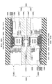
- the substrate 140A2 includes a resonator 141A2, wiring layers 142A21, 142A22, 143A2, an insulating layer 144A2, vias 145A21, 145A22, a coplanar line 146A21, a microstrip line 146A22, a coplanar line 146A23, and a connection path 147A2.
- a resonator 141A2 wiring layers 142A21, 142A22, 143A2, an insulating layer 144A2, vias 145A21, 145A22, a coplanar line 146A21, a microstrip line 146A22, a coplanar line 146A23, and a connection path 147A2.
- the coplanar line 146A21, the microstrip line 146A22, and the coplanar line 146A23 are examples of the first transmission path.
- a coplanar line, a microstrip line, and a coplanar line formed on the substrate 140B are examples of the second transmission path.
- the resonator 141A2 is a rectangular metal patch in a plan view, and a coplanar line 146A23 is connected to the center of the side on the X axis negative direction side via a connection path 147A2.
- the connection path 147A2 is a portion that penetrates into the metal patch of the rectangular resonator 141A2 in plan view.
- the connection path 147A2 is formed for impedance matching between the coplanar line 146A23 and the resonator 141A2.
- the resonator 141A2 is formed by, for example, patterning a copper foil formed on the surface of the insulating layer 144A2 on the positive side in the Z-axis so that the coplanar line 146A21, the microstrip line 146A22, the coplanar line 146A23, the connection path 147A2, and the wiring layer 142A21 and 142A22 are formed.
- the wiring layer 142A21 is formed on the lower side of the circuit device 150A, the Y-axis positive direction side and the Y-axis negative direction side of the circuit device 150A, and the X-axis positive direction side of the circuit device 150A.
- the wiring layer 142A21 is connected to the wiring layer 143A2 through the via 145A21.
- the wiring layers 142A21 and 143A2 are held at the ground potential.
- the wiring layer 142A22 is held at the ground potential and functions as a ground element.
- the wiring layer 142A22 is separated from the wiring layer 142A21.
- the wiring layer 142A22 is not formed in the section where the microstrip line 146A22 is formed in the X-axis direction.
- the wiring layer 142A22 surrounds the resonator 141A2 in plan view on the surface on the Z-axis positive direction side of the insulating layer 144A2, and is formed along both sides of the coplanar line 146A23.
- the wiring layer 142A22 is connected to the wiring layer 143A2 through the via 145A22.
- the wiring layer 143A2 is formed on the entire surface of the insulating layer 144A2 on the Z axis negative direction side.
- the wiring layer 143A2 is connected to the wiring layer 142A21 by the via 145A21 and is connected to the wiring layer 142A22 by the via 145A22, and is held at the ground potential.
- the insulating layer 144A2 is, for example, an insulating layer obtained by impregnating glass fiber with an epoxy resin when the substrate 140A2 is a printed circuit board conforming to the FR-4 standard.
- an inner wiring layer of the insulating layer 144A2 is not shown, but an inner wiring layer may be formed in the insulating layer 144A2.
- the via 145A21 connects the wiring layer 142A21 and the wiring layer 143A2.
- the via 145A21 connects the wiring layers 142A21 and 143A2 even on the lower side of the circuit device 150A.
- a number of vias 145A21 are formed so as to connect the wiring layer 142A21 and the wiring layer 143A2 over the whole in a plan view.
- the vias 145A21 are not formed in the regions indicated by the broken frame on the Y-axis positive direction side and the Y-axis negative direction side of the circuit device 150A because the terminals of the circuit device 150A are formed.
- the pitch of the vias 145A21 formed in this way is set so that, for example, the interval between adjacent vias 145A21 is less than half of the wavelength ⁇ at the communication frequency of wireless communication, and more preferably ⁇ / 4 or less.
- the via 145A22 is formed between the wiring layer 142A22 and the wiring layer 143A2, so that the via 145A22 is formed around the rectangular resonator 141A2 in plan view and on both sides of the coplanar line 146A23.
- the pitch of the vias 145A22 formed in this way is set so that, for example, the interval between adjacent vias 145A22 is less than half of the wavelength ⁇ at the communication frequency of wireless communication, and more preferably ⁇ / 4 or less.
- the end of the X-axis positive direction side of the coplanar line 146A21 is connected to the microstrip line 146A22, and the end of the X-axis negative direction side is connected to the terminal of the circuit device 150A via the bump 151A2.
- the coplanar line 146A21 is a transmission line having a characteristic impedance of 50 ⁇ , and is provided to suppress a decrease in signal transmission efficiency between the microstrip line 146A22 and the circuit device 150A.
- the coplanar line 146A21 is formed on the central axis extending in the X-axis direction of the substrate 140A2.
- the coplanar line 126A21 is formed by, for example, patterning a copper foil formed on the surface on the Z-axis positive direction side of the insulating layer 144A2, thereby microstrip line 146A22, coplanar line 146A23, connection path 147A2, resonator 141A2, and wiring layer 142A21 and 142A22 are formed.
- the coplanar line 146A21 is sandwiched between the Y axis positive direction side and the Y axis negative direction side by the wiring layer 142A21.
- the end of the X-axis negative direction side of the microstrip line 146A22 is connected to the coplanar line 146A21, and the end of the X-axis positive direction side is connected to the coplanar line 146A23.
- the microstrip line 146A22 is a transmission line having a characteristic impedance of 50 ⁇ , and is provided to suppress a decrease in signal transmission efficiency between the coplanar line 146A21 and the coplanar line 146A23.
- the coplanar line 146A23 has an end on the X-axis positive direction side connected to the resonator 141A2 via the connection path 147A2, and an end on the X-axis negative direction side connected to the microstrip line 146A22.
- the coplanar line 146A23 is a transmission line having a characteristic impedance of 50 ⁇ , and is provided to suppress a decrease in signal transmission efficiency between the resonator 141A2 and the microstrip line 146A22.
- the coplanar line 146A23 is formed on the central axis extending in the X-axis direction of the substrate 140A2.
- the coplanar line 146A23 is formed by patterning a copper foil formed on the surface on the positive side of the Z-axis of the insulating layer 144A2, thereby coplanar line 146A21, microstrip line 146A22, connection path 147A2, resonator 141A2, and wiring layer 142A21 and 142A22 are formed.
- the coplanar line 146A23 exists in a section where the wiring layer 142A2 exists on the Y axis positive direction side and the Y axis negative direction side in the X axis direction.
- the end portion on the X axis positive direction side of the coplanar line 146A23 is connected to the resonator 141A2 via the connection path 147A2.
- connection path 147A2 is a portion that penetrates into the metal patch of the rectangular resonator 141A2 in plan view.
- the connection path 147A2 is formed for impedance matching between the coplanar line 146A23 and the resonator 141A2.
- the connection path 147A2 can be regarded as a part of the resonator 141A2.
- the transmission path realized by the coplanar line 146A21, the microstrip line 146A22, and the coplanar line 146A23 is formed between the resonator 141A2 and the circuit device 150A.
- a signal output from the circuit device 150A via the bump 151A2 is transmitted to the resonator 141A2 via the coplanar line 146A21, the microstrip line 146A22, the coplanar line 146A23, and the connection path 147A2.
- the signal input to the resonator 141A2 is transmitted to the circuit device 150A via the connection path 147A2, the coplanar line 146A23, the microstrip line 146A22, and the coplanar line 146A21.
- FIG. 9 shows a cross section taken along line A3-A3 of (A).
- the cross section taken along the line A3-A3 is a cross section on the central axis extending in the X-axis direction of the substrate 140A3 shown in FIG.
- the substrate 140A3 includes a resonator 141A3, wiring layers 142A3 and 143A3, an insulating layer 144A3, a via 145A3, a coplanar line 146A31, a microstrip line 146A32, and a connection path 147A3.
- the coplanar line 146A31 and the microstrip line 146A32 are examples of the first transmission line.
- a coplanar line and a microstrip line formed on the substrate 140B are examples of the second transmission path.
- a substrate 140A3 shown in FIG. 9 has a configuration in which the wiring layer 142A22 and the via 145A22 are removed from the substrate 140A2 shown in FIG.
- the resonator 141A3 is a rectangular metal patch in plan view, and a microstrip line 146A32 is connected to the center of the side on the negative side in the X-axis via a connection path 147A3.
- the connection path 147A3 is a portion that penetrates into the metal patch of the rectangular resonator 141A3 in plan view.
- the connection path 147A3 is formed for impedance matching between the microstrip line 146A32 and the resonator 141A3.
- the resonator 141A3 is formed together with the coplanar line 146A31, the microstrip line 146A32, the connection path 147A3, and the wiring layer 142A3, for example, by patterning a copper foil formed on the surface on the positive side in the Z-axis direction of the insulating layer 144A3.
- the wiring layer 142A3 is provided under the circuit device 150A, the Y-axis positive direction side and the Y-axis negative direction side of the circuit device 150A, and the X-axis positive direction side of the circuit device 150A. And formed.
- the wiring layer 142A3 is connected to the wiring layer 143A3 through the via 145A3.
- the wiring layers 142A3 and 143A3 are held at the ground potential.
- the wiring layer 143A3 is formed on the entire surface of the insulating layer 144A3 on the Z-axis negative direction side, like the wiring layer 143A2 shown in FIG.
- the wiring layer 143A3 is connected to the wiring layer 142A3 through the via 145A3 and is held at the ground potential.
- the insulating layer 144A3 is, for example, an insulating layer obtained by impregnating glass fiber with an epoxy resin when the substrate 140A3 is a printed circuit board conforming to the FR-4 standard.
- an inner wiring layer of the insulating layer 144A3 is not shown, but an inner wiring layer may be formed in the insulating layer 144A3.
- the via 145A3 connects the wiring layer 142A3 and the wiring layer 143A3 in the same manner as the via 145A2 shown in FIG.
- the via 145A3 connects the wiring layers 142A3 and 143A3 even on the lower side of the circuit device 150A.
- a large number of vias 145A3 are formed so as to connect the wiring layer 142A3 and the wiring layer 143A3 over the whole in a plan view.
- the vias 145A3 are not formed in the regions indicated by the dashed frames on the Y-axis positive direction side and the Y-axis negative direction side of the circuit device 150A because the terminals of the circuit device 150A are formed.
- the pitch of the vias 145A3 formed in this manner is set so that, for example, the interval between adjacent vias 145A3 is less than half of the wavelength ⁇ at the communication frequency of wireless communication, and more preferably ⁇ / 4 or less.
- the coplanar line 146A31 is connected to the microstrip line 146A32 at the end on the X-axis positive direction side, and the end on the negative X-axis side via the bump 151A3. It is connected to the terminal 150A.
- the coplanar line 146A31 is a transmission line having a characteristic impedance of 50 ⁇ , and is provided to suppress a decrease in signal transmission efficiency between the microstrip line 146A32 and the circuit device 150A.
- the coplanar line 146A31 is formed on the central axis extending in the X-axis direction of the substrate 140A3.
- the coplanar line 126A21 is formed together with the microstrip line 146A32, the connection path 147A3, the resonator 141A3, and the wiring layer 142A3, for example, by patterning a copper foil formed on the surface on the positive side in the Z-axis direction of the insulating layer 144A3.
- the coplanar line 146A31 is sandwiched between the Y axis positive direction side and the Y axis negative direction side by the wiring layer 142A3.
- the end of the X-strip negative direction side of the microstrip line 146A32 is connected to the coplanar line 146A31, and the end of the X-axis positive direction is connected to the connection path 147A3.
- the microstrip line 146A32 is a transmission line having a characteristic impedance of 50 ⁇ , and is provided to suppress a decrease in signal transmission efficiency between the coplanar line 146A31 and the connection line 147A3.
- connection path 147A3 is a portion that penetrates into the metal patch of the rectangular resonator 141A3 in plan view.
- the connection path 147A3 is formed for impedance matching between the microstrip line 146A32 and the resonator 141A3.
- the connection path 147A3 can be regarded as a part of the resonator 141A3.
- the transmission path realized by the coplanar line 146A31 and the microstrip line 146A32 is formed between the resonator 141A3 and the circuit device 150A.
- a signal output from the circuit device 150A via the bump 151A3 is transmitted to the resonator 141A3 through the coplanar line 146A31, the microstrip line 146A32, and the connection path 147A3.
- the signal input to the resonator 141A3 is transmitted to the circuit device 150A via the connection path 147A3, the microstrip line 146A32, and the coplanar line 146A31.
- the substrate 140A4 includes a resonator 141A4, wiring layers 142A4 and 143A4, an insulating layer 144A4, vias 145A41 and 145A42, and a pad 146A4.
- FIG. 11 shows the substrate 140A4 in a state where the circuit device 150A shown in FIG. 10 is removed.
- the resonator 141A4 has a pair of slots formed in the wiring layer 142A4.
- the pair of slots of the resonator 141A4 extends in the Y-axis direction and is spaced apart in the X-axis direction.
- the length in the Y-axis direction of the pair of slots of the resonator 141A4 is set to an appropriate width in accordance with the radiation characteristics, and the distance between the pair of slots is set to the half length ( ⁇ / 2) is preferable.
- the width of each of the pair of slots of the resonator 141A4 may be set to an appropriate width in accordance with the radiation characteristics of the resonator 141A4, and is preferably narrower than the thickness of the insulating layer 144A.
- the resonator 141A4 is formed together with the wiring layer 142A4 and the pad 146A4, for example, by patterning a copper foil formed on the surface on the positive side in the Z-axis direction of the insulating layer 144A4.
- the wiring layer 142A4 is held at the ground potential.
- the wiring layer 142A4 is formed on the surface of the insulating layer 144A4 on the positive side in the Z-axis direction, excluding the pair of slots of the resonator 141A4 and the pad 146A4.
- the wiring layer 142A4 is connected to the wiring layer 143A4 through the via 145A41.
- the wiring layers 142A4 and 143A4 are held at the ground potential.
- the wiring layer 142A4 is formed together with the resonator 141A4 and the pad 146A4 by patterning a copper foil formed on the surface on the positive side in the Z-axis direction of the insulating layer 144A4.
- the wiring layer 143A4 is formed on the entire surface of the insulating layer 144A4 on the Z axis negative direction side.
- the wiring layer 143A4 is connected to the wiring layer 142A4 through the via 145A41 and is held at the ground potential.
- the wiring layer 143A4 is connected to the pad 146A4 by the via 145A42.
- the insulating layer 144A4 is, for example, an insulating layer obtained by impregnating glass fiber with an epoxy resin when the substrate 140A4 is a printed circuit board conforming to the FR-4 standard.
- an inner wiring layer of the insulating layer 144A4 is not shown, but an inner wiring layer may be formed in the insulating layer 144A4.
- the via 145A41 connects the wiring layers 142A4 and 143A4.
- a large number of vias 145A41 are formed so as to connect the wiring layers 142A4 and 143A4 over the whole in a plan view.
- the via 145A41 is not formed between the resonator 141A4 and the pad 146A4.
- a portion of the wiring layer 142A4 that is located between the resonator 141A4 and the pad 146A4 in plan view and is not connected to the via 145A41 is referred to as a waveguide portion 142A41.
- the waveguide portion 142A41 and the corresponding portion of the wiring layer 143A4 constitute the waveguide 147A4.
- the via 145A41 is formed on the entire surface of the wiring layer 142A4 in plan view, excluding the waveguide portion 142A41 and the area indicated by the broken-line frame on the Y-axis positive direction side and Y-axis negative direction side of the circuit device 150A. .
- the "-" marks on the Y-axis positive direction side and the Y-axis negative direction side indicate that the via 145A41 is formed to the ends of the wiring layer 142A4 on the Y-axis positive direction side and the Y-axis negative direction side. .
- the vias 145A41 are not formed because the terminals of the circuit device 150A are formed.
- the pitch of the vias 145A41 thus formed is set so that, for example, the interval between the adjacent vias 145A41 is less than half of the wavelength ⁇ at the communication frequency of wireless communication, and more preferably ⁇ / 4 or less.
- the via 145A42 connects the pad 146A4 and the wiring layer 143A4.
- the pad 146A4 is formed at a position corresponding to the position of the terminal of the circuit device 150A, and the end on the X axis negative direction side is connected to the terminal of the circuit device 150A by the bump 151A4.
- the end of the pad 146A4 on the X axis positive direction side is connected to the wiring layer 143A4 by a via 145A42.
- the pad 146A4 is a rectangular pad that is long in the X-axis direction and short in the Y-axis direction in plan view.
- the pad 146A4 is surrounded on all sides by the wiring layer 142A4.
- the pad 146A4 is formed together with the resonator 141A4 and the wiring layer 142A4 by patterning a copper foil formed on the surface of the insulating layer 144A4 on the Z axis positive direction side. Is done.
- the via 145A42 and the pad 146A4 function as a resonator and radiate a signal transmitted from the circuit device 150A into the waveguide 147A4.
- the waveguide 147A4 is located between the resonator 141A4 and the pad 146A4 in a plan view in the wiring layer 142A4, and the waveguide 142A41 that is a portion to which the via 145A41 is not connected, and the waveguide in the wiring layer 143A4. This is a transmission path constructed by a portion corresponding to 142A41.
- the waveguide 147A4 is an example of a first transmission line.
- the waveguide formed on the substrate 140B is an example of the second transmission path.
- the waveguide 147A4 can transmit electromagnetic waves bidirectionally between the via 145A42 connected to the pad 146A4 and the resonator 141A4.
- a signal output from the circuit device 150A through the bump 151A1 is transmitted by the waveguide 147A4 through the pad 146A4 and the via 145A42.
- the signal input to the resonator 141A4 is transmitted to the via 145A442 through the waveguide 247A4, and is transmitted to the circuit device 150A through the pad 146A4 and the bump 151A4.
- the substrates 140A and 140B of the wireless communication device 100 are connected between the circuit device 150A and the resonator 141A by the transmission paths of the substrates 140A1 to 140A4 described with reference to FIGS.
- the signal transmission is possible between the circuit device 150B and the resonator 141B.
- a signal is transmitted between the resonator 121A1 and the circuit device 150A by transmitting a signal between the resonator 123A1 of the resonator 120A described with reference to FIGS. 3 and 4 and the resonator 141A. be able to.
- a signal can be transmitted between the resonator 121B1 and the circuit device 150B by transmitting a signal between the resonator 123B1 of the resonance device 120B and the resonator 141B.
- wireless communication is performed between the resonator 121A1 of the resonance device 120A and the resonator 121B1 of the resonance device 120B in a state where the wireless communication devices 100A and 100B are arranged close to each other.
- signals can be transmitted and received between the circuit devices 150A and 150B.
- the distance between the resonators 121A1 and 121B1 is set, for example, to a distance of about half ( ⁇ / 2) or one quarter ( ⁇ / 4) or less of the wavelength ( ⁇ ) at the communication frequency of wireless communication. do it. This is the distance given as a neighborhood solution.
- the resonators 121A1 and 121B1 can be coupled, and efficient signal transmission can be performed between the resonators 121A and 121B. it can.
- the wireless communication apparatus 100 when the wireless communication apparatus 100 according to the first embodiment performs data communication at a transmission rate of 1 Gbps, the communication frequency band is required to be about 1 GHz, and the carrier wave frequency is a millimeter wave band sufficiently higher than the communication frequency band.
- the communication used is advantageous.
- the distance between the resonators 121A1 and 121B1 is, for example, several millimeters to several tens of millimeters. This should be set to a degree.
- the resonator 121A is located outside the wall 110A1 of the housing 110A
- the resonator 121B is located outside the wall 110B1 of the housing 110B.
- the electromagnetic wave (signal) radiated from the resonator 121A1 reaches the resonator 121B1 without being blocked by the surrounding structure or the like.
- the electromagnetic wave (signal) radiated from the resonator 121B1 reaches the resonator 121A1 without being blocked by surrounding structures or the like.
- electromagnetic waves are efficiently transmitted between the wireless communication device 100A having the resonator 121A1 and the wireless communication device 100B having the resonator 121B1. It can be carried out.
- the wireless communication apparatus 100 it is possible to provide the wireless communication apparatus 100 with good transmission efficiency. Further, according to Embodiment 1, it is possible to provide radio communication apparatuses 100A and 100B with good transmission efficiency.
- FIG. 12 is a diagram showing a cross-sectional structure of the wireless communication device 10 of the comparative example.
- the wireless communication device 10 of the comparative example includes housings 11A and 11B, substrates 12A and 12B, antenna modules 13A1, 13A2, 13B1, and 13B2, and modules 14A1 to 14A4 and 14B1 to 14B4.
- the wireless communication device 10 of the comparative example does not perform wireless communication between the casings 110A and 110B by the resonators 121A1 and 123A1 and the like as in the wireless communication device 100 of the first embodiment, but the antenna modules 13A1 and 13A2 , 13B1 and 13B2 are used to perform wireless communication between the casings 11A and 11B.
- the casings 11A and 11B are, for example, metal casings, and have openings 11A1, 11A2, 11B1, and 11B2, respectively.
- the casings 11A and 11B are arranged close to each other in parallel.
- Boards 12A and 12B are disposed inside the casings 11A and 11B, respectively.
- the boards 12A and 12B are, for example, printed boards (PCB: Printed Circuit Circuit Board) conforming to the FR-4 (Flame Retardant Type 4) standard, and have a plurality of wiring layers disposed on the front surface, the inner layer, and the back surface. Including.
- PCB printed Circuit Circuit Board
- FR-4 Freme Retardant Type 4
- the antenna modules 13A1 and 13A2 include at least an antenna and are mounted on the substrate 12A to emit or receive electromagnetic waves.
- the antenna modules 13B1 and 13B2 have at least antennas mounted on the substrate 12B, and emit or receive electromagnetic waves.
- the antenna modules 13A1, 13A2, 13B1, and 13B2 are patch antennas, for example, and radiate electromagnetic waves radially from the radiation surface.
- the antenna modules 13A1, 13A2, 13B1, and 13B2 are referred to as antennas.
- the modules 14A1 to 14A4 and 14B1 to 14B4 are, for example, circuit devices that generate communication signals and the like, and transmit signals to and from the antennas 13A1, 13A2, 13B1, and 13B2 via the boards 12A and 12B. Do.
- the antenna 13A2 and the antenna 13B2 are arranged in the opening 11A2.
- 11B2 can transmit and receive electromagnetic waves.
- the wireless communication device 10 can perform wireless communication between the antenna 13A2 and the antenna 13B2.
- the antenna 13A2 is offset to the inside of the housing 11A from the opening 11A2 of the housing 11A.
- the antenna 13B2 is offset to the inside of the housing 11A from the opening 11A2 of the housing 11A.
- the distance between the antennas 13A2 and 13B2 is not a short distance as given by the neighborhood solution, but is a longer distance, for example, about 10 times the wavelength.
- the electromagnetic waves indicated by the arrows ⁇ 1 and ⁇ 2 are radiated from the antenna 13B2 through the opening 11B2 to the outside of the housing 11B, but do not pass through the opening 11A2 of the housing 11A, and the housings 11A and 11B. Propagates horizontally between them.
- electromagnetic waves indicated by arrows ⁇ 3 and ⁇ 4 are radiated from the antenna 13B2 and propagate through the inside of the housing 11B without passing through the opening 11B2.
- the reflected wave of the electromagnetic wave indicated by the arrow ⁇ 4 is also generated as indicated by the dashed arrow. Since this reflected wave has a delay, it directly affects the direct wave ⁇ .
- the wireless communication device 10 shown in FIG. 12 has a transmission efficiency higher than that of the wireless communication device 100 of Embodiment 1 (see FIG. 1). Not good.
- FIG. 13 is a diagram showing a wireless communication apparatus 100 according to a modification of the first embodiment.
- a recess 110A3 and a recess 110B3 are formed in the wall 110A1 of the housing 110A and the wall 110B1 of the housing 110B, respectively.
- the recess 110A3 is an example of a first recess
- the recess 110B3 is an example of a second recess.
- the concave portions 110A3 and 110B3 are portions recessed from the wall portions 110A1 and 110B1 to the inside of the housings 110A and 110B, respectively.
- the openings 110A2 and 110B2 are formed in the recesses 110A3 and 110B3.
- the distance between the wall 110A1 of the housing 110A and the wall 110B1 of the housing 110B is very short, and a distance necessary for wireless communication cannot be secured between the resonator 121A1 and the resonator 121B1. Even in this case, a longer distance can be secured between the resonator 121A1 and the resonator 121B1 by providing the recesses 110A3 and 110B3.
- the offset amount of the recesses 110A3 and 110B3 with respect to the wall portions 110A1 and 110B is the contact between the resonator 121A1 and the resonator 121B1.
- the length may be set appropriately.
- FIG. 14 is a cross-sectional view showing wireless communication apparatus 200 and electronic apparatus 520 of the second embodiment.
- the wireless communication device 200 according to the second embodiment is obtained by replacing the resonance devices 120A and 120B of the wireless communication device 100 according to the first embodiment with resonance devices 220A and 220B.
- Resonance devices 220A and 220B have a configuration in which attenuation units 210A and 210B are added to resonance devices 120A and 120B of wireless communication device 100 of the first embodiment.
- the electronic device 520 of the second embodiment is obtained by replacing the wireless communication device 100 included in the electronic device 500 of the first embodiment with the wireless communication device 200 of the second embodiment.
- wireless communication device 200 includes wireless communication devices 200A and 200B
- electronic device 520 includes electronic devices 520A and 520B.
- FIG. 15 will be used in addition to FIG.
- FIG. 15 is a plan view showing the resonator 121A and the attenuation unit 210A of the resonance device 220A of the wireless communication device 200A of the second embodiment.
- the resonance device 220A includes an attenuation unit 210A, a resonance substrate 221A, a waveguide 122A, and a resonance substrate 123A.
- the resonance device 220B includes an attenuation unit 210B, a resonance substrate 221B, a waveguide 122B, and a resonance substrate 123B.
- the resonant substrate 221A includes a resonator 121A1, a resonator 221A2, and an insulating layer 221A3.
- the insulating layer 221A3 is larger in plan view than the insulating layer 121A3 of the first embodiment.
- the resonator 221A2 includes the ground element 221A21 connected to the waveguide 122A and the ground of the resonator 121A2 of the first embodiment. Larger than the element.
- an attenuation portion 210A is formed around the resonator 121A1 of the insulating layer 221A3.
- the attenuation unit 210A may be handled as a component of the resonance substrate 221A.
- the resonant substrate 221B includes a resonator 121B1, a resonator 221B2, and an insulating layer 221B3.
- the insulating layer 221B3 is larger in plan view than the insulating layer 121B3 of the first embodiment.
- the resonator 221B2 includes a ground element 221B21 connected to the waveguide 122B, and the ground of the resonator 121B2 of the first embodiment. Larger than the element.
- an attenuation portion 210B is formed around the resonator 121B1 of the insulating layer 221B3.
- the attenuation unit 210B may be handled as a component of the resonance substrate 221B.
- the attenuation part 210A is a rectangular annular member formed concentrically around the resonator 121A1 on one surface (the lower surface in FIG. 14) of the insulating layer 221A3.
- the attenuating portion 210A is a member that attenuates electromagnetic waves and is formed so as to surround the four sides of the resonator 121A1.
- the attenuation unit 210A is a member having an electrical resistance, for example.
- the attenuation unit 210A is an example of a first attenuation unit.
- the attenuator 210A attenuates or disappears a component propagating in a planar shape from the resonator 121A1 without reaching the resonator 121B1 facing the resonator 121A1 among the electromagnetic waves radiated from the resonator 121A1.
- the attenuation unit 210A converts the electromagnetic wave propagating from the resonator 121A1 in the lateral direction (plane direction) into thermal energy or the like with resistance, and attenuates or disappears.
- the attenuating unit 210A only needs to attenuate the electromagnetic wave propagating from the resonator 121A1 in the lateral direction (plane direction) to a power level that does not cause an adverse effect on the surroundings without completely disappearing.
- FIG. 16 is a plan view showing an exemplary configuration of the attenuation unit 210A of the wireless communication apparatus 200A of the second embodiment.
- the attenuation part 210A includes, for example, a plurality of metal resonance pattern units 210A1 formed in a rectangular annular region around the resonator 121A1 on one surface (the lower surface in FIG. 14) of the insulating layer 221A3. It is.
- the metal resonance pattern unit 210A1 is formed concentrically around the resonator 121A1 on one surface (the lower surface in FIG. 14) of the insulating layer 221A3, and the distance between the centers of each metal resonance pattern unit 210A1 is the same length. It is arranged periodically. A resonance pattern in which a metal layer is formed is arranged in the metal resonance pattern unit 210A1.
- FIG. 16 shows 128 metal resonance pattern units 210A1.
- the 128 metal resonance pad pattern units 210A1 are periodically patterned in a lattice shape as shown in FIG.
- the resonators of the metal resonance pattern unit 210A1 are periodically arranged to function to attenuate and absorb electromagnetic waves in a desired frequency band, that is, in the wireless carrier frequency band.
- a metal pattern periodically arranged to suppress transmission at a specific frequency is also called an EBG (Electromagnetic Band-Gap) structure.
- EBG Electromagnetic Band-Gap
- Such a metal resonance pattern unit 210A1 is formed by, for example, lasing a rectangular annular metal layer formed concentrically around the resonator 121A1 on one surface (the lower surface in FIG. 14) of the insulating layer 221A3 by laser processing or the like. It can form by dividing
- the metal resonance pattern unit 210A1 is realized by, for example, copper foil or aluminum foil.
- the metal resonance pattern unit 210A1 is made of copper foil, for example, etching or laser processing of a copper foil formed in a concentric rectangular shape around the resonator 121A1 on one surface (the lower surface in FIG. 14) of the insulating layer 221A3 It can be formed by patterning with the above.
- This copper foil may be the same as the copper foil for forming the resonator 121A1.
- the metal resonance pattern unit 210A1 is made of aluminum foil
- the aluminum foil is deposited by vapor deposition or the like in a rectangular annular region around the resonator 121A1 on one surface (the lower surface in FIG. 14) of the insulating layer 221A3.
- aluminum foil can be formed by patterning by laser processing or the like.
- the attenuation unit 210A formed in the resonance device 220A has been described with reference to FIGS. 15 and 16, but the same applies to the attenuation unit 210B formed in the resonance device 220B.
- the attenuation unit 210B is an example of a second attenuation unit.
- the wireless communication device 200 of the second embodiment similar to the wireless communication device 100 of the first embodiment, the wireless communication device 200A having the resonator 121A1 and the wireless communication device 200B having the resonator 121B1 It is possible to efficiently transmit electromagnetic waves (signals).
- the radio communication apparatus 200 As described above, according to the second embodiment, it is possible to provide the radio communication apparatus 200 with good transmission efficiency. Further, according to Embodiment 2, it is possible to provide radio communication apparatuses 200A and 200B with good transmission efficiency.
- the electronic device 520 including the wireless communication device 200 (200A, 200B) with good transmission efficiency.
- radio communication apparatus 200 of the second embodiment when electromagnetic waves propagate from between resonators 121A1 and 121B1 between housings 110A and 110B, attenuation units 210A and 210B. Can attenuate the electromagnetic wave.
- the radio communication apparatus 200 it is possible to provide the radio communication apparatus 200 with good transmission efficiency and better communication performance.
- the wall 110A1 of the housing 110A and the wall 110B1 of the housing 110B is about an integral multiple of the wavelength ⁇ at the communication frequency of wireless communication, the wall It is possible to suppress the occurrence of resonance between the portions 110A1 and 110B1.
- the wireless communication device 200 with further improved communication performance by suppressing the occurrence of resonance between the wall portions 110A1 and 110B1.
- FIG. 17 is a cross-sectional view showing wireless communication apparatus 300 and electronic apparatus 530 according to Embodiment 3.
- the wireless communication device 300 according to the third embodiment is obtained by replacing the resonance devices 120A and 120B and the substrates 140A and 140B of the wireless communication device 100 according to the first embodiment with the resonance devices 320A and 320B and the substrates 340A and 340B.
- Resonance devices 320A and 320B are different from resonance devices 120A and 120B of the first embodiment in that they are mounted on substrates 340A and 340B, respectively.
- the electronic device 530 of the third embodiment is obtained by replacing the wireless communication device 100 included in the electronic device 500 of the first embodiment with the wireless communication device 300 of the third embodiment.
- the wireless communication device 300 includes wireless communication devices 300A and 300B.
- the wireless communication device 300A includes a housing 310A and a resonance device 320A.
- the wireless communication device 300B includes a housing 310B and a resonance device 320B.
- the electronic device 530 of Embodiment 3 includes an electronic device 530A and an electronic device 530B.
- the electronic device 530A includes a wireless communication device 300A, a substrate 130A, a substrate 340A, and a circuit device 150A.
- the electronic device 530B includes a wireless communication device 300B, a substrate 130B, a substrate 340B, and a circuit device 150B.
- substrate 340A are handled as a component of the electronic device 530A here, the board
- the board 130B and the board 340B are handled as components of the electronic device 530B here, the board 130B and the board 340B may be handled as components of the wireless communication apparatus 300B. That is, the wireless communication device 300B may be handled as including the housing 310B, the resonance device 320B, the substrate 130B, and the substrate 340B.
- the housings 310A and 310B are, for example, metal housings, and have wall portions 310A1 and 310B1, respectively.
- the casings 310A and 310B are arranged side by side with the wall portions 310A1 and 310B1 in proximity to each other and in a substantially parallel state.
- the housing 310A is an example of a first housing
- the housing 310B is an example of a second housing.
- the wall portion 310A1 is an example of a first wall portion
- the wall portion 310B1 is an example of a second wall portion.
- the casings 310A and 310B have openings 310A2 and 310B2 formed in the walls 310A1 and 310B1, respectively.
- the opening 310A2 is an example of a first opening
- the opening 310B2 is an example of a second opening.
- the openings 310A2 and 310B2 are rectangular openings in plan view. From the opening 310A2, the resonator 321A2 of the resonance device 320A faces the outside of the housing 310A through the insulating layer 321A3. Further, from the opening 310B2, the resonator 321B2 of the resonance device 320B faces the outside of the housing 310B via the insulating layer 321B3.
- the sizes of the openings of the openings 310A2 and 310B2 in plan view are equal to or larger than the sizes of the resonance substrates 321A and 321B of the resonance devices 320A and 320B, respectively.
- the size of the openings 310A2 and 310B2 in plan view may be set as appropriate so as not to interfere with electromagnetic wave radiation of the resonant substrates 321A and 321B.
- FIG. 17 shows only the wall portion 310A1 in which the opening 310A2 is formed among the wall portions of the housing 310A.
- the housing 310A includes the resonance device 320A, the substrates 130A and 340A, and the circuit device 150A. It is formed so as to surround (incorporate).
- FIG. 17 shows only the wall portion 310B1 in which the opening 310B2 is formed among the wall portions of the housing 310B.
- the housing 310B includes the resonance device 320B, the substrates 130B and 340B, and the circuit device 150B. Is formed so as to surround (internally).
- the resonance devices 320A and 320B are mounted on the substrates 340A and 340B, respectively.
- the resonance device 320A includes a resonance substrate 321A and a waveguide 322A.
- the resonance device 320B includes a resonance substrate 321B and a waveguide 322B.
- the resonance device 320A is an example of a first resonance device, and the resonance device 320B is an example of a second resonance device.
- the waveguide 322A is an example of a first waveguide, and the waveguide 322B is an example of a second waveguide.
- the resonance device 320A is mounted on the substrate 140A so that the resonator 321A2 of the resonance substrate 321A faces the outside of the housing 310A from the opening 310A2.
- the waveguide 322A of the resonance device 320A may have a rectangular cross section, or may have a cross-sectional shape corresponding to FIG.
- the resonator 321A2 is an example of a first resonator.
- the resonance device 320B is mounted on the substrate 140B so that the resonator 321B2 of the resonance substrate 321B faces the outside of the housing 310B from the opening 310B2.
- the waveguide 322B of the resonance device 320B may have a rectangular cross section, or may have a cross sectional shape corresponding to FIG.
- the resonator 321B2 is an example of a second resonator.
- the resonant substrate 321A has a first surface 321A1, a resonator 321A2, and an insulating layer 321A3.
- the first surface 321A1 is a surface opposite to the surface connected to the waveguide 322A of the insulating layer 321A3, and the resonator 321A2 is formed on the surface connected to the waveguide 322A of the insulating layer 321A3. Yes.
- the first surface 321A1 is, for example, the same as the first surface in FIG. 4B, and the insulating layer 321A3 occupies the entire surface, and there is no resonator.
- the resonator 321A2 is formed, for example, by patterning a copper foil attached to the front and back surfaces of the insulating layer 321A3.
- the resonant substrate 321A transmits electromagnetic waves by the resonator 321A2.
- the radiation surface of the resonator 321A2 is located outside the housing 310A inside the opening 310A2 than the surface located inside the housing 310A of the wall portion 310A1.
- the resonator 321A2 is disposed so that the radiation surface is located outside the housing 310A with respect to the inner surface of the housing 310A.
- the resonant substrate 321B has a first surface 321B1, a resonator 321B2, and an insulating layer 321B3.
- the first surface 321B1 is a surface opposite to the surface connected to the waveguide 322B of the insulating layer 321B3, and the resonator 321B2 is formed on the surface connected to the waveguide 322B of the insulating layer 321B3. Yes.
- the first surface 321B1 occupies the entire surface of the insulating layer 321B3 as in the first surface of FIG. 4B, and there is no resonator.
- the resonator 321B2 is formed, for example, by patterning a copper foil attached to the front surface and the back surface of the insulating layer 321B3.
- the resonant substrate 321B transmits electromagnetic waves by the resonator 321B2.
- the radiation surface of the resonator 321B2 is located outside the housing 310B inside the opening 310B2 rather than the surface located inside the housing 310B of the wall portion 310B1.
- the resonator 321B2 is disposed such that the radiation surface is located outside the housing 310B with respect to the inner surface of the housing 310B.
- the waveguides 322A and 322B are constructed of, for example, a metal film molded into a rectangular tube, or, for example, (B), (C), (D), and (E) of FIG. A modified rectangular shape as shown in FIG.
- the metal film for example, a copper foil or a metal foil made of aluminum can be used. Since the inner surfaces of the waveguides 322A and 322B only have to be covered with a metal layer, a metal layer may be formed on the inner surface of a rectangular tubular or deformed rectangular resin member. Alternatively, a hollow waveguide shape having only a metal layer without an internal resin may be used.
- the metal layer may be a metal layer made of copper or aluminum, for example.
- the waveguides 322A and 322B have a configuration in which end portions 322A1 and 322B1 are added to the waveguides 122A and 122B of the first embodiment, respectively.
- Each of the end portions 322A1 and 322B1 is a rectangular annular metal layer, and has a rectangular opening in plan view.
- the waveguide 322A One end (the lower end in FIG. 17) of the waveguide 322A is connected to the resonator 321A2 of the resonance substrate 321A, and the end 322A1 at the other end (the upper terminal in FIG. 17) is soldered.
- the ball 351A is connected to the wiring layer 342A of the substrate 340A.
- the solder ball 351A may be a metal bump.
- a plurality of solder balls 351A are arranged along a rectangular annular cross section of the waveguide 322A in plan view.
- the interval between the adjacent solder balls 351A is set to be less than half of the wavelength ⁇ at the communication frequency of wireless communication, and more preferably ⁇ / 4 or less.
- the waveguide 322A forms a waveguide between the resonator 321A2 and the resonator 341A of the substrate 340A.
- the cross section of the waveguide 322A parallel to the resonance substrate 321A is rectangular.
- the waveguide 322A transmits electromagnetic waves between the resonant substrate 321A and the resonator 341A of the substrate 340A.
- one end (the upper end in FIG. 17) of the waveguide 322B is connected to the resonator 321B2 of the resonance substrate 321B, and the end 322B1 at the other end (the lower terminal in FIG. 17).
- the end 322B1 at the other end are connected to the wiring layer 342B of the substrate 340B by solder balls 351B.
- a plurality of solder balls 351B are arranged along a rectangular annular cross section of the waveguide 322B in plan view.
- the interval between the adjacent solder balls 351B is set to be less than half of the wavelength ⁇ at the communication frequency of wireless communication, and more preferably ⁇ / 4 or less.
- the waveguide 322B forms a waveguide between the resonator 321B2 and the resonator 341B of the substrate 340B.
- the cross section of the waveguide 322B parallel to the resonance substrate 321B is rectangular.
- the waveguide 322B transmits electromagnetic waves between the resonant substrate 321B and the resonator 341B of the substrate 340B.
- the substrates 130A and 130B are disposed inside the casings 310A and 310B, respectively, and the substrates 340A and 340B are mounted thereon.
- the substrates 340A and 340B are mounted on the substrates 130A and 130B inside the housings 310A and 310B, respectively.
- the boards 340A and 340B are, for example, printed boards conforming to the FR-4 standard.
- the substrate 340A is an example of a first substrate
- the substrate 340B is an example of a second substrate.
- the substrate 340A includes a resonator 341A, wiring layers 342A and 343A, an insulating layer 344A, and a via 345A.
- the resonator 341A and the wiring layers 342A and 343A are formed by patterning a copper foil attached to the front surface and the back surface of the insulating layer 344A.
- the resonator 341A transmits electromagnetic waves to and from the resonator 321A2 of the resonance device 320A.
- the wiring layers 342A and 343A are held at the ground potential.
- a circuit device 150A is mounted on the wiring layer 342A via the solder ball 151A, and an end 322A1 of the waveguide 322A is connected via the solder ball 351A.
- the substrate 340A is connected to the substrate 130A through the wiring layer 343A.
- the substrate 340B includes a resonator 341B, wiring layers 342B and 343B, an insulating layer 344B, and a via 345B.
- the resonator 341B and the wiring layers 342B and 343B are formed by patterning a copper foil attached to the front surface and the back surface of the insulating layer 344B.
- the resonator 341B transmits electromagnetic waves to and from the resonator 321B2 of the resonance device 320B.
- the wiring layers 342B and 343B are held at the ground potential.
- the circuit device 150B is mounted on the wiring layer 342B via the solder ball 151B, and the end 322B1 of the waveguide 322B is connected via the solder ball 351B.
- the substrate 340B is connected to the substrate 130B through the wiring layer 343B.
- the circuit devices 150A and 150B are flip-chip mounted on the substrates 340A and 340B by being connected to the substrates 340A and 340B via solder balls 151A and 151B, respectively, and being fixed by the underfill materials 152A and 152B.
- the circuit devices 150A and 150B are connected to the resonators 341A and 341B via the transmission lines of the substrates 340A and 340B, respectively.
- the configuration of the transmission paths of the circuit devices 150A and 150B is the same as that shown in any of FIGS. 7 to 11 in the first embodiment.
- signals can be transmitted and received between the resonator 321A2 of the wireless communication device 300A and the circuit device 150A of the electronic device 530A including the wireless communication device 300A.
- signals can be transmitted and received between the resonator 321B2 of the wireless communication device 300B and the circuit device 150B of the electronic device 530B including the wireless communication device 300B.
- Electromagnetic waves can be efficiently transmitted to and from 150B.
- the radio communication apparatus 300 As described above, according to the third embodiment, it is possible to provide the radio communication apparatus 300 with good transmission efficiency. Moreover, according to Embodiment 3, it is possible to provide radio communication apparatuses 300A and 300B with good transmission efficiency. Further, according to Embodiment 3, it is possible to provide electronic devices 530, 530A, and 530B with good transmission efficiency.
- the transmission efficiency of electromagnetic waves is improved because the radiation surfaces of the resonators 321A2 and 321B2 that perform communication between the wireless communication devices 300A and 300B are the housing 310A, This is because the wall portions 310A1 and 310B1 of the 310B are located outside the inner wall surfaces 310A11 and 310B11.
- the radiating surfaces of the resonators 321A2 and 321B2 are positioned outside the inner wall surfaces 310A11 and 310B11 of the wall portions 310A1 and 310B1, respectively, there is no object that blocks the electromagnetic waves between the resonators 321A2 and 321B2. .
- the radio communication apparatus 300 according to Embodiment 3 can obtain good transmission efficiency of electromagnetic waves.
- the resonators 321A2 and 321B2 are close enough to obtain a neighborhood solution.
- the radiation surfaces of the resonators 321A2 and 321B2 are positioned outside the housings 310A and 310B inside the openings 310A2 and 310B2 and outside the inner wall surfaces 310A11 and 310B11 of the housing 310A, respectively.
- the form is shown.
- the radiation surfaces of the resonators 321A2 and 321B2 May be located inside the casings 310A and 310B with respect to the inner wall surfaces 310A11 and 310B11.
- the positional relationship between the resonator 321A2 and the opening 310A2 can be defined so that the electromagnetic wave radiated from the resonator 321A2 is radiated from the opening 310A2 to the outside of the housing 310A without being reflected by the inner wall surface 310A11.
- the radiation surface of the resonator 321A2 may be located inside the housing 310A with respect to the inner wall surface 310A11.
- the positional relationship between the resonator 321B2 and the opening 310B2 is defined so that the electromagnetic wave radiated from the resonator 321B2 is radiated from the opening 310B2 to the outside of the housing 310B without being reflected by the inner wall surface 310B11.
- the radiation surface of the resonator 321B2 may be located inside the housing 310B with respect to the inner wall surface 310B11.
- FIG. 18 is a diagram illustrating a wireless communication apparatus 300 according to a modification of the third embodiment.
- a wireless communication device 300C according to a modification of the third embodiment is obtained by adding resonance substrates 323A and 323B to the resonance devices 320A and 320B of the wireless communication device 200 according to the second embodiment.
- the wireless communication device 300C includes wireless communication devices 300D and 300E.
- an electronic device 530C includes an electronic device 530D and an electronic device 530E.
- a resonance device 320A shown in FIG. 18 includes a resonance substrate 321A, a waveguide 322A, and a resonance substrate 323A.
- a resonance device 320A shown in FIG. 18 includes a resonance substrate 323A instead of the end 322A1 of the resonance device 320A shown in FIG.
- the resonant substrate 323A includes a ground element 323A11, a resonator 323A2, an insulating layer 323A3, and a via 323A4.
- the resonant substrate 323A is connected to the other end (the upper terminal in FIG. 17) of the waveguide 322A.
- the ground element 323A11 on the first surface 323A1 is connected to the wiring layer 342A via the solder ball 351A.
- the solder ball 351A may be a metal bump.
- the resonator 323A2 transmits an electromagnetic wave between the resonator 321A2 and the resonator 341A via the waveguide 322A.
- the ground element 323A11 is formed on the first surface 323A1 which is one surface (the upper surface in FIG. 18), and the resonator 323A2 is formed on the other surface (the lower surface in FIG. 18). Is formed.
- a via 323A4 is formed in the insulating layer 323A3.
- the via 323A4 is connected to the solder ball 351A via the ground element 323A11 around the first surface 323A1, whereby the waveguide 322A is held at the ground potential.
- the resonance device 320B shown in FIG. 18 includes a resonance substrate 321B, a waveguide 322B, and a resonance substrate 323B.
- a resonance device 320B shown in FIG. 18 includes a resonance substrate 323B instead of the end 322B1 of the resonance device 320B shown in FIG.
- the resonant substrate 323B includes a ground element 323B11, a resonator 323B2, an insulating layer 323B3, and a via 323B4.
- the resonant substrate 323B is connected to the other end (the lower terminal in FIG. 17) of the waveguide 322B.
- the ground element 323B11 side of the first surface 323B1 is connected to the wiring layer 342B via the solder balls 351B.
- the resonator 323B2 transmits an electromagnetic wave between the resonator 321B2 and the resonator 341B via the waveguide 322B.
- the ground element 323B11 is formed on the first surface 323B1 which is one surface (the lower surface in FIG. 18), and the resonator 323B2 is formed on the other surface (the upper surface in FIG. 18). Is formed.
- a via 323B4 is formed in the insulating layer 323B3.
- the via 323B4 is connected to the solder ball 351B via the ground element 323B11 around the first surface 323B1, whereby the waveguide 322B is held at the ground potential.
- FIGS. 19 to 22 are diagrams showing a resonance device 320A of the wireless communication device 300 according to the third embodiment.
- 20 and 22 are bottom views, and FIGS. 19 and 21 are cross-sectional views.
- 19 and 21 the resonance device 320A and the substrate 140A are shown upside down from FIG. 19 to 22, an XYZ coordinate system, which is an orthogonal coordinate system, is defined as shown.
- the resonance device 320A includes a resonance substrate 321A, a waveguide 322A, and a resonance substrate 323A.
- the substrate 340A includes a resonator 341A, wiring layers 342A and 343A, an insulating layer 344A, and a via 345A.
- the resonant substrate 321A has a resonator 321A2 and an insulating layer 321A3.
- the resonator 321A2 may have a configuration like the second surface shown in FIG.
- the first surface 321A1 is the surface of the insulating layer 321A3.
- the resonator 321A2 may have a configuration like the second surface shown in FIG.
- the resonant substrate 323A includes a ground element 323A11, a resonator 323A2, an insulating layer 323A3, and a via 323A4.
- the resonator 323A2 may be configured as shown on the second surface of FIG. 4A or FIG. 4C, for example.
- the first surface 323A1 is the surface of the insulating layer 323A3.
- first surface 323A1 and the ground element 323A11 may be configured as shown in FIG. 20, for example.
- the center of the first surface 323A1 is the surface of the insulating layer 323A3, and has an octagonal annular ground element 323A11 around it.
- the ground element 323A11 is connected to the resonator 323A2 via the via 323A4. As shown in FIG. 20, there are a plurality of vias 323A4, and the interval between adjacent vias 323A4 is set to be less than half of the wavelength ⁇ at the communication frequency of wireless communication, more preferably, ⁇ / 4 or less.
- the wiring layers 342A and 343A of the substrate 340A are connected by vias 345A, and the wiring layer 342A is connected to the ground layer of the substrate 130 (see FIG. 18) via the vias 345A and the wiring layers 343A. Is held at the ground potential.
- a plurality of solder balls 351A are arranged along the rectangular annular cross section of the waveguide 322A in plan view.
- the interval between the adjacent solder balls 351A is set to be less than half of the wavelength ⁇ at the communication frequency of wireless communication, and more preferably ⁇ / 4 or less.
- the plurality of arranged solder balls 351A may be a plurality of arranged metal bumps.
- a plurality of vias 323A4 are formed in the insulating layer 323A3 of the resonant substrate 323A, the ground element 323A11 and the resonator 323A2 are connected by the via 323A4, and the ground element 323A11 and the resonator 341A are connected by the solder ball 351A.
- the resonance device 320A and the transmission path of the substrate 340 can be connected.
- the transmission efficiency is good as in the wireless communication device 300 shown in FIG. Can be realized.
- the resonator 323A may include a larger number of vias 323A4 so as to be arranged in two rows on the inner peripheral side and the outer peripheral side.
- the wireless communication device 300C may include a larger number of solder balls 351A so as to be arranged in two rows on the inner peripheral side and the outer peripheral side.
- the board 340A of the wireless communication device 300C may include a larger number of vias 345A.
Landscapes
- Engineering & Computer Science (AREA)
- Computer Networks & Wireless Communication (AREA)
- Control Of Motors That Do Not Use Commutators (AREA)
- Waveguide Connection Structure (AREA)
- Aerials With Secondary Devices (AREA)
- Waveguide Aerials (AREA)
- Near-Field Transmission Systems (AREA)
- Signal Processing (AREA)
Abstract
L'invention concerne un dispositif de communication sans fil avec une excellente efficacité de transmission, et un dispositif électronique. Le dispositif de communication sans fil comprend un premier boîtier avec une première ouverture, un deuxième boîtier faisant face au premier boîtier et ayant une deuxième ouverture ouverte face à la première ouverture, un premier dispositif de résonance avec un premier résonateur et placé à l'intérieur du premier boîtier de façon que le premier résonateur soit orienté vers l'extérieur de la première ouverture, et un deuxième dispositif de résonance avec un deuxième résonateur et placé à l'intérieur du deuxième boîtier de façon que le deuxième résonateur soit orienté vers l'extérieur de la deuxième ouverture et fasse face au premier résonateur.
Priority Applications (3)
| Application Number | Priority Date | Filing Date | Title |
|---|---|---|---|
| PCT/JP2013/050010 WO2014106891A1 (fr) | 2013-01-04 | 2013-01-04 | Dispositif de communication sans fil et dispositif électronique |
| JP2014555404A JP6048513B2 (ja) | 2013-01-04 | 2013-01-04 | 無線通信装置、及び、電子装置 |
| US14/746,099 US9620851B2 (en) | 2013-01-04 | 2015-06-22 | Wireless communication device and electronic device |
Applications Claiming Priority (1)
| Application Number | Priority Date | Filing Date | Title |
|---|---|---|---|
| PCT/JP2013/050010 WO2014106891A1 (fr) | 2013-01-04 | 2013-01-04 | Dispositif de communication sans fil et dispositif électronique |
Related Child Applications (1)
| Application Number | Title | Priority Date | Filing Date |
|---|---|---|---|
| US14/746,099 Continuation US9620851B2 (en) | 2012-07-19 | 2015-06-22 | Wireless communication device and electronic device |
Publications (1)
| Publication Number | Publication Date |
|---|---|
| WO2014106891A1 true WO2014106891A1 (fr) | 2014-07-10 |
Family
ID=51062214
Family Applications (1)
| Application Number | Title | Priority Date | Filing Date |
|---|---|---|---|
| PCT/JP2013/050010 Ceased WO2014106891A1 (fr) | 2013-01-04 | 2013-01-04 | Dispositif de communication sans fil et dispositif électronique |
Country Status (3)
| Country | Link |
|---|---|
| US (1) | US9620851B2 (fr) |
| JP (1) | JP6048513B2 (fr) |
| WO (1) | WO2014106891A1 (fr) |
Cited By (3)
| Publication number | Priority date | Publication date | Assignee | Title |
|---|---|---|---|---|
| JP2019519138A (ja) * | 2016-05-05 | 2019-07-04 | 日本テキサス・インスツルメンツ合同会社 | Mm波近接場通信のための非接触インターフェース |
| WO2021177391A1 (fr) * | 2020-03-06 | 2021-09-10 | 株式会社デンソー | Carte à double face, dispositif radar, élément de transmission et procédé de fabrication d'élément de transmission |
| WO2021214815A1 (fr) * | 2020-04-20 | 2021-10-28 | 日本電信電話株式会社 | Antenne à circuit intégré |
Families Citing this family (3)
| Publication number | Priority date | Publication date | Assignee | Title |
|---|---|---|---|---|
| KR102624324B1 (ko) * | 2016-12-29 | 2024-01-12 | 주식회사 위츠 | 무선 전력 송신 장치 |
| US10476136B2 (en) | 2017-07-20 | 2019-11-12 | Apple Inc. | Electronic device with speaker port aligned antennas |
| KR102662537B1 (ko) | 2019-05-10 | 2024-05-02 | 삼성전자 주식회사 | 이중 대역 안테나 및 그것을 포함하는 전자 장치 |
Citations (5)
| Publication number | Priority date | Publication date | Assignee | Title |
|---|---|---|---|---|
| JP2004304624A (ja) * | 2003-03-31 | 2004-10-28 | Nippon Hoso Kyokai <Nhk> | ミリ波帯送信装置及びミリ波帯受信装置 |
| JP2005184124A (ja) * | 2003-12-16 | 2005-07-07 | Kyocera Corp | 誘電体共振器及び誘電体フィルタ並びに高周波モジュール |
| JP2008067012A (ja) * | 2006-09-06 | 2008-03-21 | Univ Of Tokushima | 高周波信号伝送装置 |
| JP2008252566A (ja) * | 2007-03-30 | 2008-10-16 | Matsushita Electric Ind Co Ltd | Av機器 |
| JP2010074794A (ja) * | 2008-09-22 | 2010-04-02 | Murata Mfg Co Ltd | カプラ及び通信装置 |
Family Cites Families (13)
| Publication number | Priority date | Publication date | Assignee | Title |
|---|---|---|---|---|
| JP3786497B2 (ja) | 1997-06-13 | 2006-06-14 | 富士通株式会社 | アンテナ素子を内蔵する半導体モジュール |
| US6879293B2 (en) * | 2002-02-25 | 2005-04-12 | Tdk Corporation | Antenna device and electric appliance using the same |
| JP4158142B2 (ja) * | 2002-07-08 | 2008-10-01 | 日本電気株式会社 | 携帯電話装置 |
| JP4318529B2 (ja) | 2003-10-24 | 2009-08-26 | 富士通株式会社 | 通信システム |
| JP4133747B2 (ja) * | 2003-11-07 | 2008-08-13 | 東光株式会社 | 誘電体導波管の入出力結合構造 |
| JP4191192B2 (ja) | 2005-12-27 | 2008-12-03 | Necインフロンティア株式会社 | 携帯端末、携帯端末におけるオーディオ機器の判別方法 |
| JP4345850B2 (ja) * | 2006-09-11 | 2009-10-14 | ソニー株式会社 | 通信システム及び通信装置 |
| JP4833192B2 (ja) * | 2007-12-27 | 2011-12-07 | 新光電気工業株式会社 | 電子装置 |
| JP5526659B2 (ja) | 2008-09-25 | 2014-06-18 | ソニー株式会社 | ミリ波誘電体内伝送装置 |
| JP5556072B2 (ja) * | 2009-01-07 | 2014-07-23 | ソニー株式会社 | 半導体装置、その製造方法、ミリ波誘電体内伝送装置 |
| JP5287390B2 (ja) | 2009-03-16 | 2013-09-11 | ソニー株式会社 | 半導体装置、伝送システム、半導体装置の製造方法及び伝送システムの製造方法 |
| JP2010252092A (ja) | 2009-04-16 | 2010-11-04 | Tyco Electronics Japan Kk | 導波管 |
| JP5644521B2 (ja) * | 2011-01-14 | 2014-12-24 | ソニー株式会社 | 信号伝送装置、及び、電子機器 |
-
2013
- 2013-01-04 JP JP2014555404A patent/JP6048513B2/ja not_active Expired - Fee Related
- 2013-01-04 WO PCT/JP2013/050010 patent/WO2014106891A1/fr not_active Ceased
-
2015
- 2015-06-22 US US14/746,099 patent/US9620851B2/en not_active Expired - Fee Related
Patent Citations (5)
| Publication number | Priority date | Publication date | Assignee | Title |
|---|---|---|---|---|
| JP2004304624A (ja) * | 2003-03-31 | 2004-10-28 | Nippon Hoso Kyokai <Nhk> | ミリ波帯送信装置及びミリ波帯受信装置 |
| JP2005184124A (ja) * | 2003-12-16 | 2005-07-07 | Kyocera Corp | 誘電体共振器及び誘電体フィルタ並びに高周波モジュール |
| JP2008067012A (ja) * | 2006-09-06 | 2008-03-21 | Univ Of Tokushima | 高周波信号伝送装置 |
| JP2008252566A (ja) * | 2007-03-30 | 2008-10-16 | Matsushita Electric Ind Co Ltd | Av機器 |
| JP2010074794A (ja) * | 2008-09-22 | 2010-04-02 | Murata Mfg Co Ltd | カプラ及び通信装置 |
Cited By (9)
| Publication number | Priority date | Publication date | Assignee | Title |
|---|---|---|---|---|
| JP2019519138A (ja) * | 2016-05-05 | 2019-07-04 | 日本テキサス・インスツルメンツ合同会社 | Mm波近接場通信のための非接触インターフェース |
| JP7069041B2 (ja) | 2016-05-05 | 2022-05-17 | テキサス インスツルメンツ インコーポレイテッド | Mm波近接場通信のための非接触インターフェース |
| JP2022105147A (ja) * | 2016-05-05 | 2022-07-12 | テキサス インスツルメンツ インコーポレイテッド | Mm波近接場通信のための非接触インターフェース |
| JP7579619B2 (ja) | 2016-05-05 | 2024-11-08 | テキサス インスツルメンツ インコーポレイテッド | Mm波近接場通信のための非接触インターフェース |
| JP2025013989A (ja) * | 2016-05-05 | 2025-01-28 | テキサス インスツルメンツ インコーポレイテッド | Mm波近接場通信のための非接触インターフェース |
| WO2021177391A1 (fr) * | 2020-03-06 | 2021-09-10 | 株式会社デンソー | Carte à double face, dispositif radar, élément de transmission et procédé de fabrication d'élément de transmission |
| JP2021139779A (ja) * | 2020-03-06 | 2021-09-16 | 株式会社デンソー | 両面基板、レーダ装置、伝送部材、および伝送部材の製造方法 |
| JP7294191B2 (ja) | 2020-03-06 | 2023-06-20 | 株式会社デンソー | 両面基板、レーダ装置、伝送部材、および伝送部材の製造方法 |
| WO2021214815A1 (fr) * | 2020-04-20 | 2021-10-28 | 日本電信電話株式会社 | Antenne à circuit intégré |
Also Published As
| Publication number | Publication date |
|---|---|
| JPWO2014106891A1 (ja) | 2017-01-19 |
| US20150288057A1 (en) | 2015-10-08 |
| JP6048513B2 (ja) | 2016-12-21 |
| US9620851B2 (en) | 2017-04-11 |
Similar Documents
| Publication | Publication Date | Title |
|---|---|---|
| CN101145638B (zh) | 无线通信装置 | |
| JP6048513B2 (ja) | 無線通信装置、及び、電子装置 | |
| US8994470B2 (en) | Circuit substrate having noise suppression structure | |
| TWI552434B (zh) | 具有天線之半導體結構 | |
| JP4980306B2 (ja) | 無線通信装置 | |
| US11509030B2 (en) | Dielectric filter and communications device | |
| US20160241288A1 (en) | Wireless communication apparatus and electronic apparatus | |
| CN108206318B (zh) | 印制电路板、光模块、以及光传输装置 | |
| US9893428B2 (en) | Direct transition from a waveguide to a buried chip | |
| US20210091442A1 (en) | Band-pass filter | |
| US20150222003A1 (en) | Microwave circuit | |
| CN114256595B (zh) | 一种电子设备 | |
| JP2004200783A (ja) | 高周波モジュール、および高周波モジュールにおけるスルーホールの配置方法 | |
| US11777204B2 (en) | Package | |
| JP7237161B2 (ja) | 無線装置の放射増強器、放射システム及び無線装置 | |
| JP6623805B2 (ja) | 無線通信装置 | |
| RU2719570C1 (ru) | Оптически-управляемый переключатель миллиметрового диапазона для структур на основе реализованного в печатной плате волновода со штырьевыми стенками (siw) | |
| US11424545B2 (en) | Antenna system | |
| JP7598490B2 (ja) | 伝送線路 | |
| US20210091242A1 (en) | Optically controlled millimeter-wave switch based on substrate integrated waveguide | |
| KR20220054156A (ko) | 고속 무선 데이터 송신을 위한 무선 기판 대 기판 상호 연결 | |
| JP7699730B2 (ja) | 多層基板及びそれを用いたアンテナ装置 | |
| RU2781757C1 (ru) | Беспроводное соединение для высокоскоростной передачи данных | |
| JP6782340B1 (ja) | 電磁波吸収ユニット及び電子回路 | |
| CN111602289A (zh) | 波导天线磁电匹配转变 |
Legal Events
| Date | Code | Title | Description |
|---|---|---|---|
| 121 | Ep: the epo has been informed by wipo that ep was designated in this application |
Ref document number: 13869938 Country of ref document: EP Kind code of ref document: A1 |
|
| ENP | Entry into the national phase |
Ref document number: 2014555404 Country of ref document: JP Kind code of ref document: A |
|
| NENP | Non-entry into the national phase |
Ref country code: DE |
|
| 122 | Ep: pct application non-entry in european phase |
Ref document number: 13869938 Country of ref document: EP Kind code of ref document: A1 |