WO2014108931A1 - Procédé de réduction de séchage irrégulier dans l'impression de couche mince à faible viscosité, et motif d'impression sur lequel ledit procédé est appliqué - Google Patents
Procédé de réduction de séchage irrégulier dans l'impression de couche mince à faible viscosité, et motif d'impression sur lequel ledit procédé est appliqué Download PDFInfo
- Publication number
- WO2014108931A1 WO2014108931A1 PCT/JP2013/000021 JP2013000021W WO2014108931A1 WO 2014108931 A1 WO2014108931 A1 WO 2014108931A1 JP 2013000021 W JP2013000021 W JP 2013000021W WO 2014108931 A1 WO2014108931 A1 WO 2014108931A1
- Authority
- WO
- WIPO (PCT)
- Prior art keywords
- film
- liquid
- printing
- pattern
- forming
- Prior art date
- Legal status (The legal status is an assumption and is not a legal conclusion. Google has not performed a legal analysis and makes no representation as to the accuracy of the status listed.)
- Ceased
Links
Images


Classifications
-
- H—ELECTRICITY
- H05—ELECTRIC TECHNIQUES NOT OTHERWISE PROVIDED FOR
- H05K—PRINTED CIRCUITS; CASINGS OR CONSTRUCTIONAL DETAILS OF ELECTRIC APPARATUS; MANUFACTURE OF ASSEMBLAGES OF ELECTRICAL COMPONENTS
- H05K3/00—Apparatus or processes for manufacturing printed circuits
- H05K3/22—Secondary treatment of printed circuits
- H05K3/28—Applying non-metallic protective coatings
-
- H—ELECTRICITY
- H10—SEMICONDUCTOR DEVICES; ELECTRIC SOLID-STATE DEVICES NOT OTHERWISE PROVIDED FOR
- H10K—ORGANIC ELECTRIC SOLID-STATE DEVICES
- H10K71/00—Manufacture or treatment specially adapted for the organic devices covered by this subclass
- H10K71/10—Deposition of organic active material
- H10K71/12—Deposition of organic active material using liquid deposition, e.g. spin coating
- H10K71/13—Deposition of organic active material using liquid deposition, e.g. spin coating using printing techniques, e.g. ink-jet printing or screen printing
- H10K71/135—Deposition of organic active material using liquid deposition, e.g. spin coating using printing techniques, e.g. ink-jet printing or screen printing using ink-jet printing
-
- H—ELECTRICITY
- H10—SEMICONDUCTOR DEVICES; ELECTRIC SOLID-STATE DEVICES NOT OTHERWISE PROVIDED FOR
- H10K—ORGANIC ELECTRIC SOLID-STATE DEVICES
- H10K71/00—Manufacture or treatment specially adapted for the organic devices covered by this subclass
- H10K71/10—Deposition of organic active material
- H10K71/12—Deposition of organic active material using liquid deposition, e.g. spin coating
- H10K71/15—Deposition of organic active material using liquid deposition, e.g. spin coating characterised by the solvent used
-
- H—ELECTRICITY
- H05—ELECTRIC TECHNIQUES NOT OTHERWISE PROVIDED FOR
- H05K—PRINTED CIRCUITS; CASINGS OR CONSTRUCTIONAL DETAILS OF ELECTRIC APPARATUS; MANUFACTURE OF ASSEMBLAGES OF ELECTRICAL COMPONENTS
- H05K2203/00—Indexing scheme relating to apparatus or processes for manufacturing printed circuits covered by H05K3/00
- H05K2203/01—Tools for processing; Objects used during processing
- H05K2203/0104—Tools for processing; Objects used during processing for patterning or coating
- H05K2203/013—Inkjet printing, e.g. for printing insulating material or resist
-
- H—ELECTRICITY
- H10—SEMICONDUCTOR DEVICES; ELECTRIC SOLID-STATE DEVICES NOT OTHERWISE PROVIDED FOR
- H10K—ORGANIC ELECTRIC SOLID-STATE DEVICES
- H10K59/00—Integrated devices, or assemblies of multiple devices, comprising at least one organic light-emitting element covered by group H10K50/00
- H10K59/80—Constructional details
- H10K59/88—Dummy elements, i.e. elements having non-functional features
Definitions
- the present invention uses an ink jet printer head and reduces the unevenness of drying, whereby a printing method capable of forming a film such as an alignment film or an insulating film formed of a low-viscosity ink with exactly the same film thickness up to the edge thereof, and the printing method It relates to the pattern to which the method is applied.
- liquid crystal display means having a great advantage of being thin, light and low in power consumption have been actively used as display devices for personal computers, television displays and mobile phones.
- a glass substrate as one part of the display device, elements such as TFTs and transparent electrodes are arranged on this glass substrate, A circuit pattern in which these are connected by fine wiring is formed.
- the circuit pattern is formed in one or more sections on a large glass substrate in accordance with the size of the display device to be manufactured.
- a film such as an alignment film or a fine wiring circuit is formed so as to cover the entire circuit pattern.
- An insulating film covering the pattern is formed.
- the region where the film is formed is a film formation region, and the region is set in advance on the glass substrate, and it is required that the film is formed in accordance with the set region.
- an infinite number of fine recesses provided on the surface of the anilox roll are filled with a film forming printing liquid such as polyimide varnish, and after that, the anilox roll has an elastic surface.
- the surface of the anilox roll is uniformly removed on the surface of the anilox roll by removing the excess film-forming printing liquid with a scraper that slides on the surface of the doctor roll or anilox roll that is pressed against the surface of the roll and scrapes off the excessive film-forming printing liquid.
- the film-forming printing liquid on the surface of the anilox roll is brought into contact with the surface of the resin printing plate wound around the plate cylinder in this state so that the film-forming printing liquid of a sufficient thickness adheres to the printing plate.
- the film forming printing liquid transferred to the surface and finally transferred by pressing the surface of the printing plate against the surface of the glass substrate placed on the stage is the glass substrate. Flexographic printing method that forms further transfer printing to the film forming region which is expected to have been the mainstream.
- flexographic printing methods can use highly viscous ink as a film-forming printing liquid, it has the feature that a film such as an alignment film or an insulating film can be formed with the same film thickness to the edge.
- a film such as an alignment film or an insulating film
- the flexographic printing method requires a printing plate that matches the product, it is necessary to produce a printing plate for each product type, and for transfer, dozens of sheets using a glass substrate that is actually used.
- Use of printing ink because it is necessary to perform a trial printing, and moreover, expensive film-forming printing liquid is scraped off by a scraper and discarded or deposited on an anilox roll or doctor roll.
- a solute (solid content) that is a film forming material is required because a predetermined amount of liquid droplets must be accurately dropped using an extremely thin nozzle (1a) provided at fine intervals on the ink jet head (1). 5 to 7% by weight is used, and a very low viscosity printing liquid for film formation is used which is added to a volatile solvent. This is because increasing the melt mass, which is a solid content, and increasing its viscosity decreases the discharge capability of the inkjet head (1) that uses the thin nozzle (1a). This is because it becomes difficult to finely control the discharge amount.
- the drying of the edge portion (5E) proceeds faster than the central portion (5c).
- the solvent in the edge proximity region (5e) along the edge portion (5E) flows into the edge portion (5E) together with the solute, and when dried in this state, the amount of solute in the edge portion (5E) increases and forms a bank.
- the amount of solute in the edge proximity region (5e) decreases and becomes thin, so-called coffee stain phenomenon occurs, and uniformity of the film thickness is impaired.
- This raised portion is indicated by a lattice portion in FIG. It should be noted that the non-uniform film thickness region obtained by adding both the edge portion (5E) and the edge proximity region (5e) cannot be used because the orientation of the liquid crystal is not constant and the image is distorted.
- the present invention has been made in view of the problems of the related art, and the present invention is a printing method capable of forming a uniform film thickness up to the edge of the film in ink-jet printing using a film-forming printing liquid having a very low viscosity. And providing a pattern to which the method is applied is a problem to be solved.
- the drying unevenness reducing method in the low-viscosity thin film printing according to claim 1 is: ⁇ A film forming region (R1) covering a circuit pattern (P) formed on a substrate (3) with a droplet (4) of a printing liquid containing a film forming solute via an inkjet nozzle (1a); It is characterized by having a predetermined interval from the film formation region (R1) and landing on the discarded pattern region (R2) provided along the film formation region (R1), and then drying the printing liquid. '' .
- Claim 2 is a printed pattern produced by the above-described method: “Film forming region covering circuit pattern (P) formed on substrate (3) with printing liquid containing film forming solute by inkjet nozzle (1a) ( The liquid film (51) formed in R1) and the liquid film (52) formed in the discarded pattern region (R2) formed at a predetermined interval with respect to the liquid film (51). It is characterized by that.
- the third aspect of the present invention relates to the liquid film (51) (52), wherein “the discard pattern region (R2) with respect to the droplet amount per unit area of the liquid film (51) in the film formation region (R1) covering the circuit pattern (P)”.
- the liquid droplet amount of the liquid film (52) is 70% or more of the liquid droplet amount per unit area of the liquid film (51) in the film formation region (R1) or a heat capacity equivalent to this. To do.
- the heating and drying process is performed.
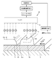
- the heat of the surface of the substrate (3) is absorbed by the liquid films (51) and (52), respectively, and the solvent is volatilized from the liquid films (51) and (52), but the liquid film between the liquid films (51) and (52) If the gap (61c) is not sufficiently narrow, the temperature of the edge (51e) of the liquid film (51) does not increase so much. Maintains substantially the same temperature as the central portion (51c) of the liquid film (51).
- the amount of solvent evaporation at the edge portion (51e) of the liquid film (51) is substantially the same as the amount of solvent evaporation at the central portion (51c) of the liquid film (51), and the coffee stain phenomenon at the edge portion (51e) is observed.
- the film thickness of the entire dried film does not occur and becomes constant.
- the amount of liquid droplets per unit area of the liquid film (52) formed in the discard pattern region (R2) is the same as that of the liquid film (51) formed in the film formation region (R1) covering the circuit pattern (P).
- the coffee stain phenomenon can be suppressed only when it becomes 70% or more.
- the amount used is preferably over 70%, a value close to this, or a heat capacity equivalent to this, and is 100% at the maximum.
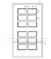
- Plan view of the printing pattern of the present invention The perspective expanded sectional view of the edge part of the printing pattern of the present invention Plan view of conventional print pattern Perspective enlarged sectional view of the edge portion of a conventional print pattern
- FIG. 1 is a schematic plan view showing an essential part of an inkjet printing apparatus for forming a film such as an alignment film and an insulating film used in the manufacturing process of a substrate (3) according to an embodiment of the present invention.
- a platen (2) on which a substrate (3) is set, and an inkjet head (1) for dropping droplets (4) for film formation into a film formation region (R1) of the substrate (3) A film thickness measurement having a transfer mechanism (15) for moving the inkjet head (1) relative to the substrate (3) on the surface plate (2), and their attached equipment, and a film thickness sensor (not shown).
- the inkjet head (1) is an inline type in which the head (1) is arranged in a direction orthogonal to the conveyance direction of the substrate (3), but of course, in a direction orthogonal to the conveyance direction of the substrate (3).
- a scanning type (not shown) in which the head (1) reciprocates may be used.
- an inline type covering the entire surface of the substrate (3) is used. In relative movement, the surface plate (2) side may move, or the head (1) side may move.
- the transfer mechanism section (15) includes a support section (not shown) that positions the inkjet head (1) above the substrate (3) by a predetermined height, and a lifting section that raises and lowers the inkjet head (1). (Not shown) and a fine adjustment unit (not shown) for finely adjusting the position of the inkjet head (1).
- the number of inkjet heads (1) may be one as shown in the figure, but in the case of a plurality, the heads (1) are arranged in parallel to each other, and a number of nozzles (1a) arranged in a line in each head (1) are the same. It is arranged with an interval of. In the case of a plurality of heads (1) as well as 1, it is preferable that each head (1) can be finely adjusted individually through horizontal movement, vertical movement and rotational movement. Further, the drive type of the ink jet head (1) may be any of a piezo type, a heater type and the like.
- the main body of the substrate (3) is a glass plate in this embodiment.
- one or a plurality of circuit patterns (P) serving as a thin film transistor display panel and a common electrode display panel paired therewith are formed thereon.
- the circuit pattern (P) of the thin film transistor panel is formed with TFT, transparent electrode, insulating film, protective film, data line, etc.
- the circuit pattern (P) of the common electrode panel is a light shielding member, color filter, cover film, common Film forming ink such as alignment film and insulating film is formed on the film forming region (R1) that covers the circuit pattern (P) and the discarded pattern region (R2) that is formed along the circuit pattern (P).
- a film is formed on it by spraying and drying it.
- a film is formed at a necessary portion.
- polyimide for example, 5 to 7% by weight of polyimide is often used as a solute material, and coated with an amide-based polar solvent such as N-methyl-2-pyrrolidone (NMP) to increase the solubility of the polyimide.
- NMP N-methyl-2-pyrrolidone
- a solution obtained by dissolving polyamic acid in a solvent such as cellosolve acetate (BC) for enhancing the properties is used.
- This is applied to the substrate (3) by ink jetting, dried, and then heat-treated at a temperature of 250 ° C. or higher to imidize the polyamic acid by thermal polymerization to form an alignment film.
- Soluble polyimide that has been imidized in a liquid state in advance instead of thermal polymerization on the substrate (3) can also be used.
- the heating temperature after coating on the substrate is sufficient for the drying process to be 180 ° C. or less, and it is suitable as an alignment film when producing a color filter substrate (3) in which the heating temperature cannot be increased.
- the alignment film made of polyimide is transparent and has high heat resistance that can withstand about 300 ° C.
- the heating method of the substrate (3) is preferable as long as the substrate (3) can be heated to a predetermined temperature so that the diameter of the droplet (4) upon landing does not greatly expand.
- an electric hot wire heater is provided in a heater table that is installed on the surface plate (2) or the surface plate body, and forms a part of the surface plate (2).
- the entire heater table is heated to a predetermined temperature, and the substrate (3) is placed on the substrate to heat the substrate (3) to a predetermined temperature and keep the temperature, the substrate
- a halogen lamp that dries by direct infrared rays from the surface side of (3). In this case, it is sufficient if the substrate (3) is heated to a predetermined temperature as described above and can be maintained at the temperature at least during ink jet printing.
- the insulating film is also formed by a similar method.
- the glass substrate (3) is provided with one or more circuit patterns (P).
- circuit patterns (P) In the case of FIG. 1, in the figure of the vertically long glass substrate (3), two rows and three stages of circuit patterns (P) are provided in the upper and lower halves, the upper half circuit pattern (P) group and the lower half circuit pattern ( A gap (61b) is formed at a wide interval with the P) group, and a narrow gap (61a) is formed between the upper and lower circuit pattern (P) groups.
- the glass substrate (3) is set on the surface plate (2) as described above.
- the surface plate (2) is heated by an internal heater (not shown), and the glass substrate (3) set on the surface plate (2) is heated to the temperature of the surface plate (2).
- the heating temperature is determined by the viscosity of the printing liquid droplets (4) and the amount of the droplets, but is 50 to 60 ° C. when the printing liquid for forming the alignment film uses the above-mentioned polyimide as a solute. If the temperature is 50 ° C. or lower, the diameter of the landed droplet (4) at the landing position will increase when landing, and the landing area at the time of landing cannot be maintained. When the temperature is 60 ° C.
- the landing area can be maintained, but the drying time is too early and the fluidity of the coalesced portion is inhibited, the linearity of the pattern edge is deteriorated, and the uniformity of the film thickness is also deteriorated.
- the elapsed time from application of the film-forming printing liquid to drying needs to be determined in consideration of the viscosity of the film-forming solution, the surface tension, the amount of solvent, and volatility. Usually, it takes about 30 to 60 seconds to dry. When the time is shorter than this time, the flatness of the film surface formed as described above is not so good, and minute film thickness unevenness occurs.
- the heating temperature of the surface plate (2) is set outside the temperature range (50 to 60 ° C.).
- the transfer mechanism is determined by the position and shape information of the circuit pattern (P) already input to the control unit (not shown) of the apparatus (A).
- the film forming area (R1) and the film forming area (R1) covering the circuit pattern (P) from the nozzle (1a) by moving the part (15) and controlling the ink jet head (1) are provided at predetermined intervals.
- a droplet (4) of the film-forming printing liquid is dropped in a set dropping pattern toward the discarded pattern region (R2).
- the heat of the surface of the substrate (3) cannot be absorbed by the liquid film (51) in the heating and drying process and the temperature rises, and the edge portion of the liquid film (51) Since the solvent evaporation amount of (51e) is larger than the solvent evaporation amount of the central portion (51c) of the liquid film (51), a discarded pattern is formed.
- the width of the gap is not constant depending on the printing conditions, but the gap between the liquid film (51) in the film formation region (R1) covering the circuit pattern (P) and the liquid film (52) in the discard pattern region (R2) is preferable. However, the width is set so that they do not flow and connect.
- the supply amount of droplets (4) of the film-forming printing liquid is 0 to 0.05 ml / min per nozzle (1a), and the droplet amount or the number of droplets can be increased or decreased in 5 to 10 steps.
- the gap is generally 5 mm or more.
- a discard pattern is formed. In FIG. 1, in this case, the discard pattern is provided over the entire length in the center of the wide gap (61b), but the liquid film (52) of the discard pattern contacts the liquid film (51) of the circuit pattern (P).
- the width not to be selected is selected. For example, if the width of the wide gap (61b) is 5 mm, the width of the liquid film (52) of the discarded pattern is 3 mm at the maximum, the liquid film (51) of the circuit pattern (P) and the liquid film of the discarded pattern ( The clearance (61c) with 52) is a minimum of 1 mm.
- a discard pattern is formed along the entire outer periphery of the circuit pattern (P) group.
- the gap (61d) and the width (for example, the maximum width of 5 mm and the minimum width of 1 mm) of the liquid film (52) of the discard pattern are set according to the above.
- liquid film (51) and the discarded pattern region (R2) of the circuit pattern (P) of the film forming solution in accordance with the film forming region (R1) and the discarded pattern region (R2) on the surface of the substrate (3).
- a liquid film (52) is formed on the surface.
- the dropping amount of the liquid film (52) is preferably 100 to 70% with respect to the dropping amount of the liquid film (51).
- the liquid film (52) to be dropped is dropped so that the heat capacity is equivalent to this.
- the dripping amount (or the heat capacity) of the liquid film (52) is 70% or less, the temperature difference between the liquid film (51) (52) portion and the gap portion becomes large and the liquid film ( 52) dries faster than the liquid film (51).
- a coffee stain phenomenon occurs at the edge portion (51e) of the liquid film (51).
- the dripping amount (or the heat capacity) of the liquid film (52) is 100% or more, the film-forming ink is expensive, and the cost is rebounded.
- the amount used is preferably a value close to 70% or more, and is 100% at the maximum. Therefore, if the dripping amount is kept within this range, even if there is a gap (61c) (61d) between the liquid films (51) (52), the gap (61c) ( The heat of 61d) is absorbed to some extent by the liquid films (51) and (52) on both sides, the temperature rise of the gap (61c) (61d) is suppressed, and the liquid film (51) (52) portion and the gap (61c) ( The temperature difference from the part 61d) becomes smaller.
Landscapes
- Engineering & Computer Science (AREA)
- Manufacturing & Machinery (AREA)
- Microelectronics & Electronic Packaging (AREA)
- Liquid Crystal (AREA)
- Manufacturing Of Printed Wiring (AREA)
Abstract
L'invention concerne un procédé d'impression par jet d'encre dans lequel un liquide d'impression de formation de film ayant une viscosité extrêmement faible est utilisé, une épaisseur de film uniforme pouvant être formée jusqu'au bord du film. Des gouttelettes (4) d'un liquide d'impression contenant un soluté de formation de film sont amenées, par l'intermédiaire d'une buse de jet d'encre (1a), à se déposer sur des régions de formation de film (R1) recouvrant un motif de circuit (P) formé sur un substrat (3) et des régions de motif factices (R2) disposées le long des régions de formation de film (R1) à une distance prédéterminée des régions de formation de film (R1). Le liquide d'impression est ensuite séché. L'apparition du phénomène de tache de café est ainsi évitée sur les sections de bord (51e) du film liquide (51), et le film séché possède une épaisseur de film entièrement uniforme.
Priority Applications (1)
| Application Number | Priority Date | Filing Date | Title |
|---|---|---|---|
| PCT/JP2013/000021 WO2014108931A1 (fr) | 2013-01-08 | 2013-01-08 | Procédé de réduction de séchage irrégulier dans l'impression de couche mince à faible viscosité, et motif d'impression sur lequel ledit procédé est appliqué |
Applications Claiming Priority (1)
| Application Number | Priority Date | Filing Date | Title |
|---|---|---|---|
| PCT/JP2013/000021 WO2014108931A1 (fr) | 2013-01-08 | 2013-01-08 | Procédé de réduction de séchage irrégulier dans l'impression de couche mince à faible viscosité, et motif d'impression sur lequel ledit procédé est appliqué |
Publications (1)
| Publication Number | Publication Date |
|---|---|
| WO2014108931A1 true WO2014108931A1 (fr) | 2014-07-17 |
Family
ID=51166615
Family Applications (1)
| Application Number | Title | Priority Date | Filing Date |
|---|---|---|---|
| PCT/JP2013/000021 Ceased WO2014108931A1 (fr) | 2013-01-08 | 2013-01-08 | Procédé de réduction de séchage irrégulier dans l'impression de couche mince à faible viscosité, et motif d'impression sur lequel ledit procédé est appliqué |
Country Status (1)
| Country | Link |
|---|---|
| WO (1) | WO2014108931A1 (fr) |
Citations (3)
| Publication number | Priority date | Publication date | Assignee | Title |
|---|---|---|---|---|
| JP2002252083A (ja) * | 2000-11-27 | 2002-09-06 | Seiko Epson Corp | 有機エレクトロルミネッセンス装置の製造方法および有機エレクトロルミネッセンス装置並びに電子機器 |
| JP2006003870A (ja) * | 2004-05-19 | 2006-01-05 | Seiko Epson Corp | カラーフィルタ基板の製造方法、電気光学装置の製造方法、電気光学装置、電子機器 |
| JP2006289239A (ja) * | 2005-04-08 | 2006-10-26 | Shibaura Mechatronics Corp | 溶液の塗布装置及び塗布方法 |
-
2013
- 2013-01-08 WO PCT/JP2013/000021 patent/WO2014108931A1/fr not_active Ceased
Patent Citations (3)
| Publication number | Priority date | Publication date | Assignee | Title |
|---|---|---|---|---|
| JP2002252083A (ja) * | 2000-11-27 | 2002-09-06 | Seiko Epson Corp | 有機エレクトロルミネッセンス装置の製造方法および有機エレクトロルミネッセンス装置並びに電子機器 |
| JP2006003870A (ja) * | 2004-05-19 | 2006-01-05 | Seiko Epson Corp | カラーフィルタ基板の製造方法、電気光学装置の製造方法、電気光学装置、電子機器 |
| JP2006289239A (ja) * | 2005-04-08 | 2006-10-26 | Shibaura Mechatronics Corp | 溶液の塗布装置及び塗布方法 |
Similar Documents
| Publication | Publication Date | Title |
|---|---|---|
| CN103676325B (zh) | 用于形成膜的方法及液晶显示装置 | |
| CN101295108A (zh) | 软烤方法 | |
| JP5113008B2 (ja) | パターン形成方法およびデバイスの形成方法 | |
| KR20130047451A (ko) | 잉크젯 프린팅 기법을 이용하여 기판의 표면에 도전성 패턴을 형성하는 방법 | |
| CN103091904B (zh) | 一种显示面板的制作方法 | |
| TW201213018A (en) | Ink-jet coating device and method | |
| KR20120052043A (ko) | 잉크젯 프린트용 기판의 표면 개질 방법 | |
| CN102224449A (zh) | 取向膜材料的滴下方法和滴下装置 | |
| CN205553568U (zh) | 一种喷墨打印机 | |
| US20160256892A1 (en) | Film coating device and film coating method using same | |
| US8777686B2 (en) | Method of jetting a liquid crystal, liquid crystal jetting apparatus for performing the method and method of manufacturing a liquid crystal panel using the apparatus | |
| WO2015113373A1 (fr) | Procédé de fabrication de film d'alignement | |
| WO2014108931A1 (fr) | Procédé de réduction de séchage irrégulier dans l'impression de couche mince à faible viscosité, et motif d'impression sur lequel ledit procédé est appliqué | |
| CN103918350A (zh) | 喷墨式喷涂装置以及喷墨式喷涂方法 | |
| KR100480826B1 (ko) | 액정표시장치의 배향막 형성장치 | |
| KR20090127694A (ko) | 평판표시소자의 패턴형성장치 및 이를 이용한 패턴형성방법 | |
| KR102011913B1 (ko) | 잉크젯 장치 | |
| CN102955374B (zh) | 玻璃基板面的快速高精度调温装置 | |
| JP5168029B2 (ja) | 印刷装置及び印刷物の製造方法 | |
| CN111190309B (zh) | 显示面板及其制备方法、转印装置 | |
| US10118318B2 (en) | Temperature regulation mask and alignment layer pre-curing device | |
| JP2006320839A (ja) | 配向膜の液滴吐出方法及び液滴吐出装置 | |
| US8431426B1 (en) | Coating method for liquid crystal alignment film of TFT-LCD | |
| JP4404046B2 (ja) | カラーフィルタ基板の製造方法および液晶表示装置の製造方法 | |
| KR101255703B1 (ko) | 액정패널 제조 방법 |
Legal Events
| Date | Code | Title | Description |
|---|---|---|---|
| 121 | Ep: the epo has been informed by wipo that ep was designated in this application |
Ref document number: 13871147 Country of ref document: EP Kind code of ref document: A1 |
|
| NENP | Non-entry into the national phase |
Ref country code: DE |
|
| 122 | Ep: pct application non-entry in european phase |
Ref document number: 13871147 Country of ref document: EP Kind code of ref document: A1 |
|
| NENP | Non-entry into the national phase |
Ref country code: JP |