WO2014109293A1 - Led装置およびその製造に用いられる塗布液 - Google Patents
Led装置およびその製造に用いられる塗布液 Download PDFInfo
- Publication number
- WO2014109293A1 WO2014109293A1 PCT/JP2014/000090 JP2014000090W WO2014109293A1 WO 2014109293 A1 WO2014109293 A1 WO 2014109293A1 JP 2014000090 W JP2014000090 W JP 2014000090W WO 2014109293 A1 WO2014109293 A1 WO 2014109293A1
- Authority
- WO
- WIPO (PCT)
- Prior art keywords
- reflective layer
- led device
- mass
- led
- substrate
- Prior art date
- Legal status (The legal status is an assumption and is not a legal conclusion. Google has not performed a legal analysis and makes no representation as to the accuracy of the status listed.)
- Ceased
Links
Images



Classifications
-
- C—CHEMISTRY; METALLURGY
- C09—DYES; PAINTS; POLISHES; NATURAL RESINS; ADHESIVES; COMPOSITIONS NOT OTHERWISE PROVIDED FOR; APPLICATIONS OF MATERIALS NOT OTHERWISE PROVIDED FOR
- C09D—COATING COMPOSITIONS, e.g. PAINTS, VARNISHES OR LACQUERS; FILLING PASTES; CHEMICAL PAINT OR INK REMOVERS; INKS; CORRECTING FLUIDS; WOODSTAINS; PASTES OR SOLIDS FOR COLOURING OR PRINTING; USE OF MATERIALS THEREFOR
- C09D183/00—Coating compositions based on macromolecular compounds obtained by reactions forming in the main chain of the macromolecule a linkage containing silicon, with or without sulfur, nitrogen, oxygen, or carbon only; Coating compositions based on derivatives of such polymers
- C09D183/04—Polysiloxanes
-
- C—CHEMISTRY; METALLURGY
- C08—ORGANIC MACROMOLECULAR COMPOUNDS; THEIR PREPARATION OR CHEMICAL WORKING-UP; COMPOSITIONS BASED THEREON
- C08K—Use of inorganic or non-macromolecular organic substances as compounding ingredients
- C08K3/00—Use of inorganic substances as compounding ingredients
- C08K3/18—Oxygen-containing compounds, e.g. metal carbonyls
- C08K3/20—Oxides; Hydroxides
- C08K3/22—Oxides; Hydroxides of metals
-
- C—CHEMISTRY; METALLURGY
- C09—DYES; PAINTS; POLISHES; NATURAL RESINS; ADHESIVES; COMPOSITIONS NOT OTHERWISE PROVIDED FOR; APPLICATIONS OF MATERIALS NOT OTHERWISE PROVIDED FOR
- C09D—COATING COMPOSITIONS, e.g. PAINTS, VARNISHES OR LACQUERS; FILLING PASTES; CHEMICAL PAINT OR INK REMOVERS; INKS; CORRECTING FLUIDS; WOODSTAINS; PASTES OR SOLIDS FOR COLOURING OR PRINTING; USE OF MATERIALS THEREFOR
- C09D5/00—Coating compositions, e.g. paints, varnishes or lacquers, characterised by their physical nature or the effects produced; Filling pastes
- C09D5/004—Reflecting paints; Signal paints
-
- F—MECHANICAL ENGINEERING; LIGHTING; HEATING; WEAPONS; BLASTING
- F21—LIGHTING
- F21V—FUNCTIONAL FEATURES OR DETAILS OF LIGHTING DEVICES OR SYSTEMS THEREOF; STRUCTURAL COMBINATIONS OF LIGHTING DEVICES WITH OTHER ARTICLES, NOT OTHERWISE PROVIDED FOR
- F21V19/00—Fastening of light sources or lamp holders
- F21V19/001—Fastening of light sources or lamp holders the light sources being semiconductors devices, e.g. LEDs
-
- F—MECHANICAL ENGINEERING; LIGHTING; HEATING; WEAPONS; BLASTING
- F21—LIGHTING
- F21V—FUNCTIONAL FEATURES OR DETAILS OF LIGHTING DEVICES OR SYSTEMS THEREOF; STRUCTURAL COMBINATIONS OF LIGHTING DEVICES WITH OTHER ARTICLES, NOT OTHERWISE PROVIDED FOR
- F21V7/00—Reflectors for light sources
- F21V7/0066—Reflectors for light sources specially adapted to cooperate with point like light sources; specially adapted to cooperate with light sources the shape of which is unspecified
-
- F—MECHANICAL ENGINEERING; LIGHTING; HEATING; WEAPONS; BLASTING
- F21—LIGHTING
- F21V—FUNCTIONAL FEATURES OR DETAILS OF LIGHTING DEVICES OR SYSTEMS THEREOF; STRUCTURAL COMBINATIONS OF LIGHTING DEVICES WITH OTHER ARTICLES, NOT OTHERWISE PROVIDED FOR
- F21V7/00—Reflectors for light sources
- F21V7/22—Reflectors for light sources characterised by materials, surface treatments or coatings, e.g. dichroic reflectors
- F21V7/24—Reflectors for light sources characterised by materials, surface treatments or coatings, e.g. dichroic reflectors characterised by the material
- F21V7/26—Reflectors for light sources characterised by materials, surface treatments or coatings, e.g. dichroic reflectors characterised by the material the material comprising photoluminescent substances
-
- F—MECHANICAL ENGINEERING; LIGHTING; HEATING; WEAPONS; BLASTING
- F21—LIGHTING
- F21V—FUNCTIONAL FEATURES OR DETAILS OF LIGHTING DEVICES OR SYSTEMS THEREOF; STRUCTURAL COMBINATIONS OF LIGHTING DEVICES WITH OTHER ARTICLES, NOT OTHERWISE PROVIDED FOR
- F21V7/00—Reflectors for light sources
- F21V7/22—Reflectors for light sources characterised by materials, surface treatments or coatings, e.g. dichroic reflectors
- F21V7/28—Reflectors for light sources characterised by materials, surface treatments or coatings, e.g. dichroic reflectors characterised by coatings
-
- H—ELECTRICITY
- H10—SEMICONDUCTOR DEVICES; ELECTRIC SOLID-STATE DEVICES NOT OTHERWISE PROVIDED FOR
- H10H—INORGANIC LIGHT-EMITTING SEMICONDUCTOR DEVICES HAVING POTENTIAL BARRIERS
- H10H20/00—Individual inorganic light-emitting semiconductor devices having potential barriers, e.g. light-emitting diodes [LED]
- H10H20/80—Constructional details
- H10H20/84—Coatings, e.g. passivation layers or antireflective coatings
- H10H20/841—Reflective coatings, e.g. dielectric Bragg reflectors
-
- C—CHEMISTRY; METALLURGY
- C08—ORGANIC MACROMOLECULAR COMPOUNDS; THEIR PREPARATION OR CHEMICAL WORKING-UP; COMPOSITIONS BASED THEREON
- C08K—Use of inorganic or non-macromolecular organic substances as compounding ingredients
- C08K3/00—Use of inorganic substances as compounding ingredients
- C08K3/18—Oxygen-containing compounds, e.g. metal carbonyls
- C08K3/20—Oxides; Hydroxides
- C08K3/22—Oxides; Hydroxides of metals
- C08K2003/2227—Oxides; Hydroxides of metals of aluminium
-
- C—CHEMISTRY; METALLURGY
- C08—ORGANIC MACROMOLECULAR COMPOUNDS; THEIR PREPARATION OR CHEMICAL WORKING-UP; COMPOSITIONS BASED THEREON
- C08K—Use of inorganic or non-macromolecular organic substances as compounding ingredients
- C08K3/00—Use of inorganic substances as compounding ingredients
- C08K3/18—Oxygen-containing compounds, e.g. metal carbonyls
- C08K3/20—Oxides; Hydroxides
- C08K3/22—Oxides; Hydroxides of metals
- C08K2003/2237—Oxides; Hydroxides of metals of titanium
- C08K2003/2241—Titanium dioxide
-
- C—CHEMISTRY; METALLURGY
- C08—ORGANIC MACROMOLECULAR COMPOUNDS; THEIR PREPARATION OR CHEMICAL WORKING-UP; COMPOSITIONS BASED THEREON
- C08K—Use of inorganic or non-macromolecular organic substances as compounding ingredients
- C08K3/00—Use of inorganic substances as compounding ingredients
- C08K3/18—Oxygen-containing compounds, e.g. metal carbonyls
- C08K3/20—Oxides; Hydroxides
- C08K3/22—Oxides; Hydroxides of metals
- C08K2003/2296—Oxides; Hydroxides of metals of zinc
-
- C—CHEMISTRY; METALLURGY
- C08—ORGANIC MACROMOLECULAR COMPOUNDS; THEIR PREPARATION OR CHEMICAL WORKING-UP; COMPOSITIONS BASED THEREON
- C08K—Use of inorganic or non-macromolecular organic substances as compounding ingredients
- C08K3/00—Use of inorganic substances as compounding ingredients
- C08K3/30—Sulfur-, selenium- or tellurium-containing compounds
- C08K2003/3045—Sulfates
-
- C—CHEMISTRY; METALLURGY
- C08—ORGANIC MACROMOLECULAR COMPOUNDS; THEIR PREPARATION OR CHEMICAL WORKING-UP; COMPOSITIONS BASED THEREON
- C08K—Use of inorganic or non-macromolecular organic substances as compounding ingredients
- C08K3/00—Use of inorganic substances as compounding ingredients
- C08K3/38—Boron-containing compounds
- C08K2003/382—Boron-containing compounds and nitrogen
-
- F—MECHANICAL ENGINEERING; LIGHTING; HEATING; WEAPONS; BLASTING
- F21—LIGHTING
- F21Y—INDEXING SCHEME ASSOCIATED WITH SUBCLASSES F21K, F21L, F21S and F21V, RELATING TO THE FORM OR THE KIND OF THE LIGHT SOURCES OR OF THE COLOUR OF THE LIGHT EMITTED
- F21Y2115/00—Light-generating elements of semiconductor light sources
- F21Y2115/10—Light-emitting diodes [LED]
-
- H—ELECTRICITY
- H10—SEMICONDUCTOR DEVICES; ELECTRIC SOLID-STATE DEVICES NOT OTHERWISE PROVIDED FOR
- H10H—INORGANIC LIGHT-EMITTING SEMICONDUCTOR DEVICES HAVING POTENTIAL BARRIERS
- H10H20/00—Individual inorganic light-emitting semiconductor devices having potential barriers, e.g. light-emitting diodes [LED]
- H10H20/80—Constructional details
- H10H20/85—Packages
- H10H20/855—Optical field-shaping means, e.g. lenses
- H10H20/856—Reflecting means
-
- H—ELECTRICITY
- H10—SEMICONDUCTOR DEVICES; ELECTRIC SOLID-STATE DEVICES NOT OTHERWISE PROVIDED FOR
- H10W—GENERIC PACKAGES, INTERCONNECTIONS, CONNECTORS OR OTHER CONSTRUCTIONAL DETAILS OF DEVICES COVERED BY CLASS H10
- H10W72/00—Interconnections or connectors in packages
- H10W72/01—Manufacture or treatment
- H10W72/015—Manufacture or treatment of bond wires
- H10W72/01515—Forming coatings
-
- H—ELECTRICITY
- H10—SEMICONDUCTOR DEVICES; ELECTRIC SOLID-STATE DEVICES NOT OTHERWISE PROVIDED FOR
- H10W—GENERIC PACKAGES, INTERCONNECTIONS, CONNECTORS OR OTHER CONSTRUCTIONAL DETAILS OF DEVICES COVERED BY CLASS H10
- H10W72/00—Interconnections or connectors in packages
- H10W72/071—Connecting or disconnecting
- H10W72/075—Connecting or disconnecting of bond wires
-
- H—ELECTRICITY
- H10—SEMICONDUCTOR DEVICES; ELECTRIC SOLID-STATE DEVICES NOT OTHERWISE PROVIDED FOR
- H10W—GENERIC PACKAGES, INTERCONNECTIONS, CONNECTORS OR OTHER CONSTRUCTIONAL DETAILS OF DEVICES COVERED BY CLASS H10
- H10W74/00—Encapsulations, e.g. protective coatings
Definitions
- the present invention relates to an LED device and a coating solution used for manufacturing the LED device.
- white LED devices in which a phosphor such as a YAG phosphor is disposed in the vicinity of a gallium nitride (GaN) blue LED (Light Emitting Diode) chip have been widely used.
- the blue light emitted from the blue LED chip and the yellow light emitted from the phosphor receiving the blue light are mixed to obtain white light.
- a white LED device in which a phosphor emitting green or red fluorescence is arranged in the vicinity of a blue LED chip has also been developed.
- the blue light emitted from the blue LED chip and the red light and the green light emitted from the phosphor receiving the blue light are mixed to obtain white light.
- White LED devices have various uses, and in recent years, white devices have been replaced with fluorescent lamps and incandescent lamps. A large number of white LED devices are arranged inside such an illumination device. Therefore, how to increase the light extraction efficiency of each white LED device is important from the viewpoint of cost reduction and long life of the lighting device. Similarly, in the case of not only a white LED device but also a monochromatic LED device that does not use a phosphor, it is important to increase the light extraction efficiency.
- the conventional LED device has a problem that the substrate on which the LED element is mounted easily absorbs the light from the LED element and the fluorescence from the phosphor, and the light extraction property is difficult to increase. Therefore, an LED device has been developed in which a reflector having a high light reflectance is disposed around the LED element. Such a reflector is generally formed of metal plating or the like.
- Patent Document 1 a reflector in which metal plating is coated with a resin layer
- Patent Document 2 a reflector in which metal plating is coated with a white resin layer
- the silicone resin has a relatively high heat resistance.
- the silicone resin has a relatively low glass transition point, and its linear expansion coefficient changes abruptly at the glass transition point. Therefore, when the metal reflector is covered with the silicone resin, there is a problem that the silicone resin is easily peeled off from the metal reflector due to a temperature change outside the LED device.
- an object of the present invention is to provide an LED device having a reflective layer that can reflect light efficiently over a long period of time with little thermal deterioration, and a coating liquid used for manufacturing the reflective layer.
- An LED device comprising: a substrate; an LED element disposed on the substrate; and a reflective layer disposed at least around the LED element on the substrate, wherein the reflective layer comprises a white pigment, polysiloxane
- the reflective layer comprises a white pigment, polysiloxane
- the LED device according to 1 above wherein the amount of bifunctional silicon contained in the polysiloxane is 40% by mass or less based on the amount of total silicon contained in the polysiloxane. 3. 3. The LED device according to 1 or 2 above, wherein the reflective layer further contains metal oxide fine particles. 4). 4. The LED device according to 3 above, wherein the metal oxide fine particles have an average particle size smaller than that of a white pigment. 5. The LED device according to any one of 1 to 4, wherein the reflective layer further contains inorganic particles. 6). 6. The LED device according to any one of 1 to 5, wherein the reflective layer further contains a clay mineral. 7). 7.
- the clay mineral contains at least one selected from the group consisting of layered clay minerals, allophane, and imogolite. 8).
- the reflective layer further contains a silane coupling agent.
- the white pigment is at least one selected from the group consisting of titanium oxide, aluminum oxide, barium sulfate, zinc oxide, and boron nitride. 10.
- the content of the white pigment contained in the reflective layer is 50% by mass or more and 95% by mass or less. 11. 2.
- a coating solution used for manufacturing a reflective layer of an LED device wherein the coating solution contains a white pigment and a polysiloxane precursor, and a reflective layer that is a cured film of the coating solution is formed at 1000 ° C. at 180 ° C.
- the reflectance reduction rate of the light having a wavelength of 500 nm is 10% or less with respect to the reflectance before holding at 180 ° C.
- the reflection layer has a thickness of ⁇ 70 to 150.
- an LED device capable of efficiently extracting light over a long period of time and a coating liquid used for manufacturing the LED device with little deterioration of a reflective layer for reflecting light emitted from an LED element. Provided.
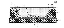
- FIG. 1 shows a top view of an example of an LED device 100A of the present invention.
- FIG. 2 shows a cross-sectional view of an example of the LED device 100A of the present invention.
- the LED element 2 will be described by taking a wire bonding type as an example.
- the LED device 100 ⁇ / b> A includes a substrate 1, an LED element 2 disposed on the substrate 1, and a reflective layer 21 disposed at least around the LED element 2 on the substrate 1. .
- the LED device 100 ⁇ / b> A may include a wavelength conversion layer 11 that covers the LED element 2 and the reflective layer 21.
- the LED element 2 may be disposed on the bottom surface 1 a of the truncated cone-shaped cavity (concave portion) of the substrate 1.
- the LED element 2 is electrically connected to a metal part (metal electrode part) 3 disposed on the substrate 1 via a wiring 4.
- the reflective layer 21 is disposed on the substrate 1 excluding the region where the LED elements 2 are disposed.
- the reflective layer 21 is arranged in a mortar shape continuously from the bottom surface 1 a to the side surface 1 b of the truncated cone-shaped cavity (concave portion) of the substrate 1.
- the reflection layer 21 is formed in a ring shape concentric with the wavelength conversion layer 11 on the outer periphery of the wavelength conversion layer 11 in a top view.
- the substrate 1 preferably has insulating properties and heat resistance, and is preferably made of a ceramic resin or a heat resistant resin.
- the heat resistant resin include liquid crystal polymer, polyphenylene sulfide, aromatic nylon, epoxy resin, hard silicone resin, polyphthalic acid amide and the like.
- the substrate 1 may contain an inorganic filler.
- the inorganic filler can be titanium oxide, zinc oxide, alumina, silica, barium titanate, calcium phosphate, calcium carbonate, white carbon, talc, magnesium carbonate, boron nitride, glass fiber, and the like.
- the wavelength of light emitted from the LED element 2 is not particularly limited.
- the LED element 2 may be, for example, an element that emits blue light (light of about 420 nm to 485 nm) or an element that emits ultraviolet light.
- the configuration of the LED element 2 is not particularly limited.
- the LED element 2 is an element that emits blue light
- the LED element 2 includes an n-GaN compound semiconductor layer (cladding layer), an InGaN compound semiconductor layer (light emitting layer), and a p-GaN compound semiconductor layer. It may be a laminate in which (clad layer) and a transparent electrode layer are laminated.
- the LED element 2 may have a light emitting surface of 200 to 300 ⁇ m ⁇ 200 to 300 ⁇ m, for example.
- the height of the LED element 2 is usually about 50 to 200 ⁇ m. In the LED device 100 shown in FIGS. 1 and 2, only one LED element 2 is disposed on the substrate 1, but a plurality of LED elements 2 may be disposed on the substrate 1.
- the reflective layer 21 is a layer that reflects the emitted light of the LED element 2 and the fluorescence emitted by the phosphor contained in the wavelength conversion layer 11 to the light extraction surface side of the LED device 100A.
- the reflective layer 21 may be formed on the surface of the substrate 1 at least outside the area where the LED elements 2 are arranged, and may be formed outside the area where the LED elements 2 are arranged.
- the arrangement region of the LED element 2 refers to a light emitting surface of the LED element 2 and a connection part between the LED element 2 and the metal part (metal electrode part) 3. That is, the reflective layer 21 is formed in a region that does not hinder the emission of light from the LED element 2 and the connection between the LED element 2 and the metal part (metal electrode part) 3.
- the reflective layer 21 is preferably formed in at least the peripheral region of the LED element 2.
- the reflective layer 21 is also formed on the side surface 1b of the cavity.
- the reflective layer 21 is formed on the side surface 1b of the cavity, the light traveling in the horizontal direction on the surface of the wavelength conversion layer 11 can be reflected by the reflective layer 21 and extracted from the light extraction surface. That is, the amount of light extracted from the light extraction surface of the LED device 100 increases.
- the thickness of the reflective layer 21 is preferably 5 to 50 ⁇ m, more preferably 5 to 30 ⁇ m. If the thickness of the reflective layer 21 is 50 ⁇ m or less, the reflective layer 21 is unlikely to crack. On the other hand, when the thickness of the reflective layer 21 is 5 ⁇ m or more, the light reflectivity of the reflective layer 21 is likely to be sufficiently increased, and the light extraction efficiency is likely to be enhanced.
- the reduction rate of the reflectance of light having a wavelength of 500 nm of the reflective layer 21 when held at 180 ° C. for 1000 hours is 10% or less with respect to the reflectance before holding at 180 ° C.
- the reduction rate of the reflectance is preferably 5% or less, and more preferably 2% or less.
- the reflectance reduction rate is [(reflectance of reflection layer before holding at 180 ° C. ⁇ reflectance of reflection layer after holding at 180 ° C. for 1000 hours) / (reflectance of reflection layer before holding at 180 ° C.)] ] ⁇ 100.
- Each reflectance is measured with a spectrophotometer.
- the reflectance reduction rate is as follows: (i) Prepare a sample in which a film having the same composition and the same thickness as the reflective layer is formed on a transparent glass plate, and (ii) the sample at 180 ° C. It may be calculated by holding for 1000 hours. Further, the reduction rate may be calculated by directly measuring the reflectance of the reflective layer included in the LED device.
- the use environment temperature of the high-luminance lighting device and the in-vehicle lighting device is about -40 ° C to 120 ° C. Therefore, when the LED device is applied to these lighting devices, the resin contained in the reflective layer is likely to deteriorate due to heat in the use environment, light from the LED element, and heat, and light extraction from the LED device is reduced. There was a case.
- the reflective layer 21 of the LED device 100A of the present invention is held at 180 ° C. for a long time as described above, the reflectance of the reflective layer does not greatly decrease. Therefore, a good light extraction property from the LED device 100A is maintained for a long time.
- the reflectance of the reflective layer 21 is adjusted by the type of polysiloxane included in the reflective layer 21 and the like.
- 180 degreeC is a heat-resistant limit temperature of a general LED element.
- the reflective layer 21 of the LED device 100A of the present invention does not have a glass transition point in the range of ⁇ 70 to 150 ° C. Therefore, the physical properties of the reflective layer 21 are not easily changed even by heat or cold air in the usage environment of the LED device, and high adhesion between the substrate 1 and the reflective layer 21 is easily maintained.
- the glass transition point of the reflective layer 21 may be less than ⁇ 70 ° C. or higher than 150 ° C., but the glass transition point is preferably higher than 150 ° C., more preferably 160 ° C. or higher.
- the glass transition point of the reflective layer 21 is adjusted by the composition of polysiloxane contained in the reflective layer 21.
- the glass transition point of the reflective layer 21 is measured by the TMA method (thermomechanical analysis method) based on JIS K7197. Specifically, the temperature is measured at a rate of ⁇ 100 ° C. to 10 ° C./min with a thermomechanical measurement device. This may be a value obtained by preparing a sample in which a film having the same composition and the same thickness as the reflective layer is formed on a transparent glass plate, and measuring the glass transition point of the sample. Further, the glass transition point of the reflective layer included in the LED device may be directly measured.
- TMA method thermomechanical analysis method
- the reflective layer 21 of the LED device 100A of the present invention is a layer in which a white pigment is bound with polysiloxane, and electricity is not conducted. Therefore, in the LED device 100A of the present invention, the reflective layer 21 can be formed in any region of the substrate 1 and can be formed in a gap between the metal portions 3 or the like. That is, the formation area of the reflective layer 21 can be increased, and the light extraction efficiency from the LED device 100A can be increased.
- the reflective layer 21 of the present invention includes a white pigment and polysiloxane, but also includes metal oxide fine particles, inorganic particles, clay minerals, and a silane coupling agent as necessary.
- metal oxide fine particles inorganic particles, clay minerals, and a silane coupling agent as necessary.
- the white pigment contained in the reflective layer 21 is not particularly limited as long as it is a highly reflective particle.
- White pigments are calcium carbonate, magnesium carbonate, barium carbonate, magnesium sulfate, barium sulfate, calcium sulfate, zinc oxide, magnesium oxide, calcium oxide, titanium oxide, aluminum oxide, zirconium oxide, zinc sulfide, aluminum hydroxide, boron nitride, It can be aluminum nitride, potassium titanate, barium titanate, aluminum titanate, strontium titanate, calcium titanate, magnesium titanate, hydroxyapatite, and the like. These may be included in the reflective layer 21 alone or in combination of two or more.
- the white pigment is particularly preferably a mixture of titanium oxide, aluminum oxide, barium sulfate, zinc oxide, boron nitride, or a combination thereof.
- the thermal conductivity of the reflective layer 21 tends to increase. As a result, the heat generated from the LED element can be quickly released from the reflective layer 21 to the outside of the LED device 100A. Therefore, the temperature of the LED device 100A is kept low, and the lifetime of the LED device is prolonged.
- the average primary particle size of the white pigment is preferably more than 100 nm and not more than 20 ⁇ m, more preferably more than 100 nm and not more than 10 ⁇ m, still more preferably from 200 nm to 2.5 ⁇ m.
- the “average primary particle size” refers to the value of D50 measured with a laser diffraction particle size distribution meter.
- Examples of the laser diffraction particle size distribution measuring device include a laser diffraction particle size distribution measuring device manufactured by Shimadzu Corporation.
- the amount of the white pigment contained in the reflective layer 21 is preferably 50 to 95% by mass, and more preferably 70 to 90% by mass with respect to the total mass of the reflective layer.
- the amount of the white pigment is 50% by mass or more, the light reflectivity of the reflective layer 21 is likely to be sufficient, and the light extraction efficiency is sufficiently increased.
- the amount of the white pigment exceeds 95% by mass, the amount of the binder (polysiloxane) is relatively decreased, and the strength of the reflective layer 21 may be lowered, or the white pigment may be missing from the surface.
- the polysiloxane contained in the reflective layer 21 can be a bifunctional silane compound, a trifunctional silane compound, or a polymer (cured product) of a tetrafunctional silane compound monomer or oligomer thereof.
- the amount of polysiloxane contained in the reflective layer 21 is preferably 5 to 50% by mass and more preferably 10 to 40% by mass with respect to the total mass of the reflective layer.
- the amount of polysiloxane is less than 5% by mass, the white pigment is not sufficiently retained, and pigment powder tends to be generated on the surface.
- the amount of polysiloxane exceeds 40% by mass, the reflective layer 21 may be cracked due to curing shrinkage.
- the amount of bifunctional silicon contained in the polysiloxane is preferably 40% by mass or less, more preferably 25% by mass or less, based on the total amount of silicon contained in the polysiloxane. More preferably, it is 15 mass% or less.
- Bifunctional silicon refers to silicon derived from a bifunctional silane compound.
- the amount of bifunctional silicon is 40% by mass or less, the glass transition point of the reflective layer 21 tends to increase to 150 ° C. or higher.
- the amount of bifunctional silicon exceeds 40% by mass, the amount of organic groups contained in the polysiloxane increases. Therefore, the hydroxyl group on the surface of the substrate 1 and the silicon in the polysiloxane are hardly bonded, and the adhesion between the substrate 1 and the reflective layer 21 tends to be lowered.
- the amount of tetrafunctional silicon (silicon derived from a tetrafunctional silane compound) contained in polysiloxane is 0 to 300 parts by mass with respect to 100 parts by mass of trifunctional silicon (silicon derived from a trifunctional silane compound). Preferably, it is 0 to 200 parts by mass, and more preferably 0 to 100 parts by mass.
- the tetrafunctional silane compound is contained in the polysiloxane, the silicon in the polysiloxane and the hydroxyl group on the surface of the substrate 1 are easily bonded, and the adhesion between the substrate 1 and the reflective layer 21 is likely to be increased.
- the amount of the tetrafunctional silane compound is excessive, the degree of cross-linking of the polysiloxane increases, and cracks may occur in the reflective layer 21.
- the mass ratio of bifunctional silicon, trifunctional silicon, and tetrafunctional silicon contained in the reflective layer 21 is determined by solid Si-nuclear magnetic resonance (hereinafter referred to as “NMR: Nuclear Magnetic Resonance”). A solid Si-NMR spectrum will be described.
- polysiloxane containing tetrafunctional silicon as a main component is represented by the SiO 2 ⁇ nH 2 O formula, but structurally, oxygen atoms O are bonded to each vertex of a silicon atom Si tetrahedron. These oxygen atoms O have a structure in which silicon atoms Si are further bonded and spread in a net shape.
- the following schematic diagram (A) shows the Si—O net structure ignoring the tetrahedral structure.
- the schematic diagram (B) in the repeating unit of Si—O—Si—O— in the schematic diagram (A), a part of the Si—O bond is substituted with another member (for example, —H, —CH 3, etc.). It represents something.
- the silicon atom Si (Q 4 ) having four —OSi as shown in the schematic diagram (B)
- the peaks based on the respective silicon atoms Si are sequentially called Q 4 peak, Q 3 peak,...
- Q 4 peak tetrafunctional silicons
- Q sites tetrafunctional silicons
- Q 0 to Q 4 peaks derived from the Q site are referred to as a Q n peak group.
- the Q n peak group of the silica film containing no organic substituent is usually observed as a multimodal peak continuous in the region of ⁇ 80 to ⁇ 130 ppm chemical shift.
- trifunctional silicon that is, silicon derived from a trifunctional silane compound in which three oxygen atoms are bonded and one other atom (usually carbon) is bonded generally has a T site.
- the peak derived from the T site is observed as each peak of T 0 to T 3 as in the case of the Q site.
- each peak derived from the T site is referred to as a Tn peak group.
- the T n peak group is generally observed as a multimodal peak continuous in a region on the higher magnetic field side (usually chemical shift of ⁇ 80 to ⁇ 40 ppm) than the Q n peak group.
- bifunctional silicon that is, silicon derived from a bifunctional silane compound in which two oxygen atoms are bonded and two other atoms (usually carbon) are bonded is generally referred to as a D site. Is done.
- the peak derived from the D site is also observed as each peak of D 0 to D n (D n peak group), which is further than the peak group of Q n and T n. It is observed as a multimodal peak in the region on the high magnetic field side (usually the region with a chemical shift of ⁇ 3 to ⁇ 40 ppm).
- monofunctional silicon silicon derived from a monofunctional silane compound in which one oxygen atom is bonded and three other atoms (usually carbon atoms) are bonded is generally an M site.
- FIG. 7 is an example of the Si-NMR spectrum of polysiloxane.
- the horizontal axis represents the chemical shift
- the vertical axis represents “relative strength” depending on the abundance of the compound having each structure.
- D11 indicates actual measurement data.
- D12 represents data modeled by a Gaussian function.
- D13 shows the difference spectrum.
- the peak P11 (chemical shift near ⁇ 20.0 ppm) is the D n peak group
- the peak P12 (chemical shift near ⁇ 60.0 ppm) is the T n peak group
- the peak P13 (chemical shift) shift -100.0 ⁇ -110 ppm vicinity) is Q n peak group.
- the polysiloxane includes bifunctional silicon, trifunctional silicon, and tetrafunctional silicon.
- the area ratio of each of these peak groups of D n , T n , and Q n is equal to the mass ratio (molar ratio) of silicon atoms placed in the environment corresponding to each peak group. Therefore, if the total mass of all the silicon contained the area of all peaks in the polysiloxane (molar amount), Q n peak group, T n peak group, it is contrasted with the area of the D n peak group and M n peak group Thus, how much bifunctional silicon, trifunctional silicon, and tetrafunctional silicon are included is calculated.
- bifunctional silane compound examples include a compound represented by the following general formula (II).
- R 5 each independently represents an alkyl group or a phenyl group, preferably an alkyl group having 1 to 5 carbon atoms or a phenyl group.
- R 4 represents a hydrogen atom or an alkyl group.
- bifunctional silane compound examples include dimethoxysilane, diethoxysilane, dipropoxysilane, dipentyloxysilane, diphenyloxysilane, methoxyethoxysilane, methoxypropoxysilane, methoxypentyloxysilane, methoxyphenyloxysilane, ethoxypropoxy.
- Trifunctional silane compound examples include a compound represented by the following general formula (III).
- R 1 Si (OR 2 ) 3 (III) In the above general formula, each R 2 independently represents an alkyl group or a phenyl group, and preferably represents an alkyl group having 1 to 5 carbon atoms or a phenyl group.
- R 1 represents a hydrogen atom or an alkyl group.
- trifunctional silane compounds include trimethoxysilane, triethoxysilane, tripropoxysilane, tripentyloxysilane, triphenyloxysilane, dimethoxymonoethoxysilane, diethoxymonomethoxysilane, dipropoxymonomethoxysilane, di Propoxymonoethoxysilane, dipentyloxylmonomethoxysilane, dipentyloxymonoethoxysilane, dipentyloxymonopropoxysilane, diphenyloxylmonomethoxysilane, diphenyloxymonoethoxysilane, diphenyloxymonopropoxysilane, methoxyethoxypropoxysilane, monopropoxydimethoxysilane Monopropoxydiethoxysilane, monobutoxydimethoxysilane, monopentyloxydiethoxysilane, monofluoro Monohydrosilane compounds such as nyloxydieth
- R 1 represented by the general formula (III) of these trifunctional silane compounds is a methyl group
- the hydrophobicity of the surface of the reflective layer 21 is lowered.
- the composition for forming the wavelength conversion layer easily spreads and the adhesion between the wavelength conversion layer 11 and the reflective layer 21 is increased.
- the trifunctional silane compound in which R 1 represented by the general formula (III) is a methyl group include methyltrimethoxysilane and methyltriethoxysilane, and methyltrimethoxysilane is particularly preferable.
- each R 3 independently represents an alkyl group or a phenyl group, and preferably represents an alkyl group having 1 to 5 carbon atoms or a phenyl group.
- tetrafunctional silane compounds include tetramethoxysilane, tetraethoxysilane, tetrapropoxysilane, tetrabutoxysilane, tetrapentyloxysilane, tetraphenyloxysilane, trimethoxymonoethoxysilane, dimethoxydiethoxysilane, and triethoxymonomethoxy.
- Silane trimethoxymonopropoxysilane, monomethoxytributoxysilane, monomethoxytripentyloxysilane, monomethoxytriphenyloxysilane, dimethoxydipropoxysilane, tripropoxymonomethoxysilane, trimethoxymonobutoxysilane, dimethoxydibutoxysilane, Triethoxymonopropoxysilane, diethoxydipropoxysilane, tributoxymonopropoxysilane, dimethoxymonoethoxymonobutoxy Silane, diethoxymonomethoxymonobutoxysilane, diethoxymonopropoxymonobutoxysilane, dipropoxymonomethoxymonoethoxysilane, dipropoxymonomethoxymonobutoxysilane, dipropoxymonoethoxymonobutoxysilane, dipropoxymonoethoxymonobutoxysilane, dipropoxymonoethoxymonobutoxy
- the polysiloxane may be a polymer of an oligomer of a silane compound.
- the oligomer of the silane compound for obtaining the polysiloxane is obtained by mixing the above-mentioned bifunctional silane compound, trifunctional silane compound, and tetrafunctional silane compound in a desired ratio and reacting them in the presence of an acid catalyst, water, and a solvent. It is done. The molecular weight of the oligomer is adjusted by the reaction time, temperature, water concentration, and the like.
- the oligomer preferably has a weight average molecular weight of 500 to 20000 as measured by GPC (gel permeation chromatograph), more preferably 1000 to 10,000, and even more preferably 1500 to 6000.
- GPC gel permeation chromatograph
- solvents for preparing oligomers include monohydric alcohols such as methanol, ethanol, propanol and n-butanol; alkyl carboxylic acid esters such as methyl-3-methoxypropionate and ethyl-3-ethoxypropionate; ethylene Polyhydric alcohols such as glycol, diethylene glycol, propylene glycol, glycerin, trimethylolpropane, hexanetriol; ethylene glycol monomethyl ether, ethylene glycol monoethyl ether, ethylene glycol monopropyl ether, ethylene glycol monobutyl ether, diethylene glycol monomethyl ether, diethylene glycol monoethyl Ether, diethylene glycol monopropyl ether, diethylene glycol monobutyl ether, pro Monoethers of polyhydric alcohols such as lenglycol monomethyl ether, propylene glycol monoethyl ether, propylene glycol monopropyl ether, propylene glycol
- the reflective layer 21 may contain metal oxide fine particles having an average particle size smaller than that of the white pigment, for example, metal oxide fine particles having an average particle size of 5 nm or more and less than 100 nm.
- metal oxide fine particles having an average particle size of 5 nm or more and less than 100 nm.
- the linear expansion coefficient of the reflective layer 21 is reduced.
- good adhesion between the reflective layer 21 and the substrate 1 is maintained even when a thermal history having a significant temperature difference is received.
- irregularities are generated on the surface of the reflective layer 21, and an anchor effect is exhibited between the reflective layer 21 and the wavelength conversion layer 11 formed thereon. As a result, the adhesion between the reflective layer and the wavelength conversion layer is greatly enhanced.
- the stress (for example, the stress caused by polycondensation or drying of polysiloxane) generated during the formation of the reflective layer 21 is relieved by the metal oxide fine particles. Therefore, cracks are less likely to occur when the reflective layer 21 is formed.
- metal oxide fine particles is not particularly limited, but from the viewpoint of being relatively easily available, aluminum oxide, zirconium oxide, zinc oxide, tin oxide, yttrium oxide, cerium oxide, titanium oxide, copper oxide, and One or more metal oxide fine particles selected from the group consisting of bismuth oxide are preferred.
- the average primary particle size of the metal oxide fine particles is more preferably 5 to 80 nm, and further preferably 5 to 50 nm in consideration of the respective effects described above. By setting the average primary particle size in such a range, fine irregularities are generated on the surface of the reflective layer 21, and the anchor effect described above can be obtained.
- the average primary particle size of the metal oxide fine particles is measured, for example, by a Coulter counter method.
- the metal oxide fine particles may be porous, and the specific surface area is preferably 200 m 2 / g or more. When the metal oxide fine particles are porous, impurities are adsorbed in the porous voids.
- the amount of the metal oxide fine particles contained in the reflective layer 21 is preferably 0.1 to 20% by mass, and more preferably 5 to 10% by mass with respect to the total mass of the reflective layer. If the amount of the metal oxide fine particles is too small, the above-described anchor effect is not sufficient. On the other hand, if the amount of metal oxide fine particles is excessive, the amount of polysiloxane is relatively decreased, and the strength of the reflective layer 21 may not be sufficiently increased.
- the reflective layer 21 may contain inorganic particles having an average particle diameter of 100 nm to 100 ⁇ m.
- inorganic particles When inorganic particles are contained in the reflective layer 21, the linear expansion coefficient of the reflective layer 21 is reduced. As a result, good adhesion between the reflective layer 21 and the substrate 1 is maintained even when a thermal history having a significant temperature difference is received. Moreover, since the gap between the white pigment and the other particles is filled, the strength of the reflective layer 21 is likely to increase. Furthermore, if the coating liquid for forming the reflective layer 21 contains inorganic particles, the viscosity of the coating liquid is likely to increase and the applicability of the coating liquid is likely to increase.
- the average particle diameter of the inorganic particles is preferably 100 nm or more and 50 ⁇ m or less, more preferably 1 ⁇ m or more and 30 ⁇ m or less, from the viewpoint of filling a gap generated at the interface between the white pigment particles and other particles.
- the average particle diameter of the inorganic particles can be measured, for example, by a Coulter counter method.
- the inorganic particles include oxide particles such as silicon oxide, aluminum oxide, and zirconium oxide, fluoride particles such as magnesium fluoride, or a mixture thereof.
- the inorganic particles are preferably oxide particles, and from the viewpoint of the stability of the reflective layer 21 with respect to the binder (polysiloxane), the oxide particles are preferably silicon oxide.
- the amount of inorganic particles contained in the reflective layer 21 is preferably 0 to 20% by mass, more preferably 5 to 10% by mass, based on the total mass of the reflective layer. When inorganic particles are contained, the adhesion between the reflective layer 21 and the substrate 1 is likely to increase.
- the reflective layer 21 may contain clay mineral. When clay mineral is contained in the reflective layer 21, the linear expansion coefficient of the reflective layer 21 is reduced. As a result, good adhesion between the reflective layer 21 and the substrate 1 is maintained even when a thermal history having a significant temperature difference is received.
- clay minerals include layered silicate minerals, imogolite and allophane.
- the layered silicate mineral is preferably a swellable clay mineral having a mica structure, a kaolinite structure, or a smectite structure, and particularly a swellable clay mineral having a smectite structure rich in swelling properties.
- layered silicate minerals include natural or synthetic hectrite, saponite, stevensite, hydelite, montmorillonite, nontritite, bentonite and other smectite genus clay minerals; Swellable mica clay minerals such as fluorine mica, Na type fluorine teniolite, Li type fluorine teniolite; and vermiculite; kaolinite; or mixtures thereof.
- Examples of commercial products of clay minerals include Laponite XLG (synthetic hectorite analogues manufactured by LaPorte, UK), Laponite RD (synthetic hectorite analogues manufactured by LaPorte, UK), Thermabis (Synthetic hectorite, Henkel, Germany) Light-like substance), smecton SA-1 (saponite-like substance manufactured by Kunimine Industry Co., Ltd.), Bengel (natural bentonite sold by Hojun Co., Ltd.), Kunivia F (natural montmorillonite sold by Kunimine Industry Co., Ltd.), Veegum (USA) , Natural hectorite manufactured by Vanderbilt), Daimonite (synthetic swellable mica manufactured by Topy Industries, Ltd.), Micromica (synthetic non-swellable mica manufactured by Coop Chemical Co., Ltd.), Somasifu (Coop Chemical Co., Ltd.) Synthetic swelling mica), SWN (synthetic
- the amount of clay mineral contained in the reflective layer 21 is preferably 0 to 20% by mass, more preferably 5 to 10% by mass, based on the total mass of the reflective layer. When clay minerals are included, the adhesion between the reflective layer 21 and the substrate 1 is likely to increase.
- the reflective layer 21 may contain a silane coupling agent.
- silane coupling agent included in the reflective layer 21, the adhesion between the substrate 1 and the reflective layer 21 is enhanced, and the durability of the LED device 100A is enhanced.
- silane coupling agent examples include vinyltrimethoxysilane, vinyltriethoxysilane, 2- (3,4-epoxycyclohexyl) ethyltrimethoxysilane, 3-glycidoxypropyltrimethoxysilane, and 3-glycidoxypropyl.
- the amount of the silane coupling agent contained in the reflective layer is preferably 1 to 10% by mass, and more preferably 3 to 7% by mass with respect to the total mass in the reflective layer 21. If the amount of the silane coupling agent is too small, the adhesion between the reflective layer 21 and the substrate 1 is difficult to increase. On the other hand, if the silane coupling agent is excessive, the heat resistance of the reflective layer 21 may decrease.
- the reflective layer 21 may contain a metal alkoxide or metal chelate cured product (reactant) containing a metal element other than the Si element.
- the metal in the metal alkoxide or metal chelate forms a metalloxane bond with the above-described polysiloxane and the hydroxyl group present on the surface of the substrate 1 or the wavelength conversion layer 11 when the reflective layer is formed. Since the metalloxane bond is very strong, when these cured products (reactants) are included in the reflective layer 21, the adhesion between the substrate 1, the wavelength conversion layer 11 and the reflective layer 21 is increased.
- a part of the metal alkoxide or metal chelate forms a nano-sized cluster composed of a metalloxane bond in the reflective layer 21. Due to the photocatalytic effect of this cluster, a highly corrosive sulfide gas or the like existing in the vicinity of the LED device 100A is oxidized to change to a less corrosive sulfur dioxide gas or the like.
- the metal element contained in the metal alkoxide or metal chelate is preferably a group 4 or group 13 metal element other than Si, and a compound represented by the following general formula (V) is preferable.
- M m + X n Y mn (V) M represents a group 4 or group 13 metal element (excluding Si), and m represents the valence of M (3 or 4).
- X represents a hydrolyzable group, and n represents the number of X groups (an integer of 2 or more and 4 or less). However, m ⁇ n. Y represents a monovalent organic group.
- the group 4 or group 13 metal element represented by M is preferably aluminum, zirconium, or titanium, and particularly preferably zirconium.
- a cured product of zirconium alkoxide or chelate does not have an absorption wavelength in a light emission wavelength region (particularly blue light (wavelength 420 to 485 nm)) of a general LED element. That is, the light from the LED element 2 is not easily absorbed by the cured product.
- the hydrolyzable group represented by X may be a group that is hydrolyzed with water to form a hydroxyl group.
- the hydrolyzable group include a lower alkoxy group having 1 to 5 carbon atoms, an acetoxy group, a butanoxime group, a chloro group and the like.
- all the groups represented by X may be the same group or different groups.
- the hydrolyzable group represented by X is hydrolyzed and released during the formation of the reflective layer. Therefore, the compound produced after hydrolysis from the group represented by X is preferably neutral and light boiling. Therefore, the group represented by X is preferably a lower alkoxy group having 1 to 5 carbon atoms, more preferably a methoxy group or an ethoxy group.
- the monovalent organic group represented by Y may be a monovalent organic group contained in a general silane coupling agent. Specifically, the aliphatic group, alicyclic group, aromatic group, fatty acid having 1 to 1000 carbon atoms, preferably 500 or less, more preferably 100 or less, further preferably 40 or less, and particularly preferably 6 or less. It may be a ring aromatic group.
- the organic group represented by Y may be an aliphatic group, an alicyclic group, an aromatic group, or a group in which an alicyclic aromatic group is bonded via a linking group.
- the linking group may be an atom such as O, N, or S, or an atomic group containing these.
- the organic group represented by Y may have a substituent.
- substituents include halogen atoms such as F, Cl, Br, and I; vinyl group, methacryloxy group, acryloxy group, styryl group, mercapto group, epoxy group, epoxycyclohexyl group, glycidoxy group, amino group, cyano group, Organic groups such as nitro group, sulfonic acid group, carboxy group, hydroxy group, acyl group, alkoxy group, imino group and phenyl group are included.
- metal alkoxide or metal chelate represented by the general formula (V) include aluminum triisopropoxide, aluminum tri-n-butoxide, aluminum tri-t-butoxide, aluminum triethoxide and the like.
- metal alkoxide or metal chelate of zirconium represented by the general formula (V) include zirconium tetramethoxide, zirconium tetraethoxide, zirconium tetra n-propoxide, zirconium tetra i-propoxide, zirconium tetra n- Examples include butoxide, zirconium tetra-i-butoxide, zirconium tetra-t-butoxide, zirconium dimethacrylate dibutoxide, dibutoxyzirconium bis (ethylacetoacetate) and the like.
- metal alkoxide or metal chelate of the titanium element represented by the general formula (V) include titanium tetraisopropoxide, titanium tetra n-butoxide, titanium tetra i-butoxide, titanium methacrylate triisopropoxide, titanium tetra Examples include methoxypropoxide, titanium tetra n-propoxide, titanium tetraethoxide, titanium lactate, titanium bis (ethylhexoxy) bis (2-ethyl-3-hydroxyhexoxide), titanium acetylacetonate and the like.
- metal alkoxides or metal chelates exemplified above are a part of commercially available organometallic alkoxides or metal chelates.
- Metal alkoxides or metal chelates shown in the list of coupling agents and related products in Chapter 9 “Optimum Utilization Technology of Coupling Agents” published by the National Institute of Science and Technology are also applicable to the present invention.
- the cured product (reactant) of the metal alkoxide or metal chelate is preferably contained in an amount of 1 to 10% by mass, more preferably 2 to 7% by mass, based on the total mass of the reflective layer. If these amounts are too small, it is difficult to obtain the effect of improving the adhesion described above.
- the LED device 100 may include the wavelength conversion layer 11.
- the wavelength conversion layer 11 may be a layer in which phosphor particles are dispersed in a transparent resin.
- the wavelength conversion layer 11 is usually formed so as to cover the LED element 2 and the reflective layer 21.
- the wavelength conversion layer 11 receives light (excitation light) emitted from the LED element 2 and emits fluorescence. By mixing the excitation light and the fluorescence, the color of the light from the LED device 100 becomes a desired color. For example, when the light from the LED element 2 is blue and the fluorescence emitted from the phosphor included in the wavelength conversion layer 11 is yellow, the light from the LED device 100 is white.
- the transparent resin contained in the wavelength conversion layer 11 is not particularly limited, and may be, for example, a silicone resin and an epoxy resin.
- the phosphor particles contained in the wavelength conversion layer 11 may be anything that is excited by the light emitted from the LED element 2 and emits fluorescence having a wavelength different from that of the emitted light from the LED element 2.
- examples of phosphor particles that emit yellow fluorescence include YAG (yttrium, aluminum, garnet) phosphors.
- the YAG phosphor receives blue light (wavelength 420 nm to 485 nm) emitted from the blue LED element, and emits yellow fluorescence (wavelength 550 nm to 650 nm).
- the phosphor particles are, for example, 1) An appropriate amount of flux (fluoride such as ammonium fluoride) is mixed with a mixed raw material having a predetermined composition, and pressed to form a molded body. 2) The obtained molded body is packed in a crucible and fired in air at a temperature range of 1350 to 1450 ° C. for 2 to 5 hours to obtain a sintered body.
- flux fluoride such as ammonium fluoride
- a mixed raw material having a predetermined composition is obtained by sufficiently mixing stoichiometric ratios of oxides such as Y, Gd, Ce, Sm, Al, La, and Ga, or compounds that easily become oxides at high temperatures. It is done. Moreover, the mixed raw material which has a predetermined composition mixes the solution which dissolved the rare earth element of Y, Gd, Ce, and Sm in the acid by the stoichiometric ratio, and oxalic acid, and obtains a coprecipitation oxide. 2) It can also be obtained by mixing this coprecipitated oxide with aluminum oxide or gallium oxide.
- the kind of the phosphor is not limited to the YAG phosphor, and may be another phosphor such as a non-garnet phosphor that does not contain Ce.
- the average particle diameter of the phosphor particles is preferably 1 ⁇ m to 50 ⁇ m, and more preferably 10 ⁇ m or less.
- the particle diameter of the phosphor particles is too large, a gap generated at the interface between the phosphor particles and the transparent resin (epoxy resin or silicone resin) becomes large. Thereby, the intensity
- the average particle diameter of the phosphor particles can be measured, for example, by a Coulter counter method.
- the amount of the phosphor particles contained in the wavelength conversion layer 11 is generally 5 to 15% by mass with respect to the total solid content of the wavelength conversion layer.
- the thickness of the wavelength conversion layer 11 is generally 25 ⁇ m to 5 mm.
- the wavelength conversion layer 11 prepares a composition for forming a wavelength conversion layer in which phosphor particles are dispersed in a transparent resin, and this is applied onto the LED element 2 and the reflective layer 21 with a dispenser or the like. Then, it is obtained by hardening this composition for wavelength conversion layer formation.
- Coating Solution A coating solution used for manufacturing the reflective layer 21 of the LED device 100A will be described.
- the coating liquid contains a white pigment and a polysiloxane precursor (a monomer of the above-described silane compound or an oligomer thereof).
- the reflective layer which is a cured film of the coating solution, has a 10% decrease in reflectance of light having a wavelength of 500 nm when held at 180 ° C. for 1000 hours with respect to the reflectance before being held at 180 ° C. % Or less, preferably 5% or less, and more preferably 2% or less.
- the reflective layer which is a cured film of the coating solution, does not have a glass transition point in the range of ⁇ 70 to 150 ° C.
- the glass transition point of the reflective layer is measured by raising the temperature at a rate of ⁇ 100 ° C. to 10 ° C./min with a thermomechanical measuring device.
- the coating liquid contains a polysiloxane precursor (the aforementioned silane compound or oligomer thereof) and a white pigment. If necessary, an organic solvent, water, the above-described metal oxide fine particles, inorganic particles, clay mineral, silane coupling agent, metal alkoxide, metal chelate, and the like are included.
- the viscosity of the coating solution is likely to increase, and the coating property of the coating solution is increased.
- the amount of inorganic particles contained in the coating solution is preferably 0.1 to 10% by mass, and more preferably 0.2 to 5% by mass with respect to the total amount of the coating solution. When the inorganic particles are 0.1% by mass or more, a thickening effect is easily obtained.
- the coating solution contains at least one clay mineral selected from the group consisting of layered silicate minerals, imogolite and allophane. These particles have a very large surface area. And it is easy to form a card house structure in the coating liquid in a stationary state. When clay minerals form a card house structure, the viscosity of the coating solution increases significantly. On the other hand, the card house structure is apt to collapse when a certain pressure is applied, whereby the viscosity of the coating solution is lowered. That is, when clay mineral is contained in the coating solution, the viscosity of the coating solution increases in a stationary state, and the viscosity of the coating solution decreases when a certain pressure is applied. That is, when a clay mineral is contained in the coating solution, the white pigment does not easily settle in the stationary coating solution, and the coating solution is easily applied from the coating device during coating.
- the amount of the clay mineral contained in the coating solution is preferably 0.1 to 5% by mass, and more preferably 0.2 to 2% by mass with respect to the entire coating solution.
- the amount of the clay mineral is small, the viscosity of the coating solution is difficult to increase, and the white pigment tends to settle.
- the amount of the clay mineral is excessive, the viscosity of the coating solution may be excessively increased, and the coating solution may not be discharged uniformly from the coating device.
- the organic solvent contained in the coating solution contains a monohydric alcohol or a dihydric or higher polyhydric alcohol.
- the monohydric alcohol is contained, the wet spread of the coating film is improved and the coating liquid is easily applied.
- polyhydric alcohol is contained in the coating solution, the viscosity of the coating solution is likely to increase, and the white pigment is difficult to settle.
- monohydric alcohols examples include methanol, ethanol, propanol, butanol and the like.
- the amount of monohydric alcohol is preferably 10 to 50% by mass, and more preferably 20 to 40% by mass with respect to the entire coating solution.
- the polyhydric alcohol may be either a diol or a triol.
- the polyhydric alcohol include ethylene glycol, propylene glycol, diethylene glycol, glycerin, 1,3-butanediol, 1,4-butanediol and the like.
- the polyhydric alcohol is preferably ethylene glycol, propylene glycol, 1,3-butanediol, or 1,4-butanediol.
- the amount of the polyhydric alcohol contained in the coating solution is preferably 10 to 50% by mass, and more preferably 20 to 40% by mass with respect to the entire coating solution.
- the coating solution may contain water.
- water When water is contained in the coating solution, water enters between the layers of the clay mineral, the clay mineral swells, and the viscosity of the coating solution tends to increase.
- the method of preparing the coating solution is not particularly limited, and a white pigment and a polysiloxane precursor (the above-mentioned silane compound or oligomer thereof), and if necessary, an organic solvent, water, metal oxide fine particles, inorganic particles, clay mineral , A silane coupling agent or the like may be mixed at once, or may be divided into a plurality of times and mixed.
- the white pigment is preferably dispersed at least once by the following apparatus.
- the white pigment is dispersed with the following apparatus, aggregation of the pigment particles is reduced, and a denser and highly reflective reflective layer is easily obtained.
- the coating solution it is possible to disperse one or both of the inorganic particles and the clay mineral in an organic solvent or water with the following apparatus, and then mix the remaining components. preferable.
- Examples of devices that stir the mixture and / or disperse each component include magnetic stirrers, ultrasonic dispersion devices, homogenizers, stirring mills, blade kneading and stirring devices, thin-film swirling dispersers, high-pressure impact dispersers, and rotational revolutions.
- a mixer etc. are included.
- stirring device examples include Ultra Tarrax (manufactured by IKA Japan), TK homomixer (manufactured by Primix), TK pipeline homomixer (manufactured by Primics), TK Fillmix (manufactured by Primix), Claremix ( M Technic Co., Ltd.), Claire SS5 (M Technic Co., Ltd.), Cavitron (Eurotech Co., Ltd.), Fine Flow Mill (Pacific Kiko Co., Ltd.), Medialess Stirrer, Visco Mill (Imex Co., Ltd.), Apex Mill (Manufactured by Kotobuki Kogyo Co., Ltd.), Star Mill (manufactured by Ashizawa, Finetech), DMPA / S Super Flow (manufactured by Nihon Eirich), MP Mill (manufactured by Inoue Seisakusho), spike mill (manufactured by Inoue Seisakusho), Mighty mill (Inoue) Mfg.), SC mill (Mitsui
- Nanomizer manufactured by Yoshida Kikai
- a high-pressure impact type dispersing device such as NANO 3000 (manufactured by Bitsubusha).
- the stirring device may be a rotating and revolving mixer such as Awatori Nertaro (new key), an ultrasonic dispersion device, or the like.
- the coating method of the coating solution is not particularly limited, and may be a coating method using a general coating device such as a dispenser, a jet dispenser, or a spray device. Further, the curing method and curing conditions of the coating solution are appropriately selected depending on the type of polysiloxane precursor. An example of the curing method is heat curing.
- the film obtained from the coating solution is hardly cracked, and even when the film is exposed to a high temperature, the reflectance is hardly lowered. Therefore, although the said coating liquid is suitable as a coating liquid for forming the reflection layer of the above-mentioned LED device, the use of a coating liquid will not be restrict
- the configuration of the LED device 100A is not particularly limited, and various configurations can be taken.
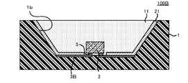
- the LED element 2 is not limited to the wire bonding type, for example, as shown in FIG. 3, a metal part (metal electrode part) 3B disposed on the substrate 1 and a flip connected via the protruding electrode 5 It may be a chip type.
- the shape of the cavity shown in FIGS. 1 and 2 is not particularly limited, and may be, for example, a truncated pyramid shape, a columnar shape, a prismatic shape, or the like.
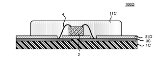
- the substrate 1 may be a flat substrate 1C as shown in FIGS. 4 and 5, for example.
- the reflective layer 21 ⁇ / b> D may be formed not only in the peripheral region of the LED element 2 but also between the substrate 1 ⁇ / b> C and the LED element 2. That is, the LED element 2 may be disposed on the reflective layer 21D. Since the reflection layer 21D is also formed between the substrate 1C and the LED element 2, the reflection layer 21D reflects the light that travels to the back surface side of the LED element 2, so that the light extraction efficiency from the LED device 100D is increased.
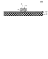
- the reflective layer 21E may not be covered with the wavelength conversion layer 11E.
- the LED device may include a wavelength conversion layer 11E that covers at least the LED element 2.
- a bifunctional silane compound, a trifunctional silane compound, a tetrafunctional silane compound, water, an acid (catalyst) and the like were mixed in the following composition to prepare a silane compound solution containing a polysiloxane precursor (oligomer). Furthermore, solid Si-NMR measurement was performed on polysiloxane obtained by heat-curing (polymerizing) the polysiloxane precursor (oligomer) at 150 ° C. And the ratio of the bifunctional silicon amount with respect to the total silicon amount contained in polysiloxane was computed. The ratio is shown in Table 1.
- Silane compound solution 1 Tetramethoxysilane 3.2% by mass, methyltrimethoxysilane 6.8% by mass, methanol 35% by mass, acetone 35% by mass, water 19.99% by mass, nitric acid 0.01% by mass, Mix and stir at 23 ° C. for 3 hours. Then, it was made to react, stirring at 26 degreeC for 3 days, and the silane compound solution 1 containing a polysiloxane precursor (oligomer) was obtained. When the molecular weight of the obtained oligomer was measured by GPC, the weight average molecular weight in terms of polystyrene was 1800. In addition, when solid Si-NMR was measured using a solid obtained by curing the solution at 150 ° C. as a sample, peaks corresponding to the Q component and the T component were observed, and no peak of the D component was observed. .
- Silane compound solution 2 Tetraethoxysilane 4.33% by weight, methyltrimethoxysilane 2.85% by weight, dimethyldimethoxysilane 2.82% by weight, methanol 70% by weight, water 19.99% by weight, nitric acid 0.01% by weight % And the mixture was stirred at 23 ° C. for 3 hours. Then, it was made to react, stirring at 26 degreeC for 3 days, and the silane compound solution 2 containing a polysiloxane precursor (oligomer) was obtained. When the molecular weight of the obtained oligomer was measured by GPC, the weight average molecular weight in terms of polystyrene was 2000.
- solid Si-NMR measurement was performed using a solid obtained by curing the solution at 150 ° C. as a sample, and peaks corresponding to the Q component, the T component, and the D component were observed.
- the ratio of the amount of bifunctional silicon to the total amount of silicon contained in the polysiloxane was 36% by mass.
- Silane compound solution 3 4% by mass of tetraethoxysilane, 2.63% by mass of methyltrimethoxysilane, 3.37% by mass of dimethyldimethoxysilane, 70% by mass of methanol, 19.99% by mass of water, 0.01% by mass of nitric acid, , And stirred at 23 ° C. for 3 hours. Then, it was made to react, stirring for 3 days at 26 degreeC, and the silane compound solution 3 containing a polysiloxane precursor (oligomer) was obtained. When the molecular weight of the obtained oligomer was measured by GPC, the weight average molecular weight in terms of polystyrene was 1800.
- solid Si-NMR measurement was performed using a solid obtained by curing the solution at 150 ° C. as a sample, and peaks corresponding to the Q component, the T component, and the D component were observed.
- the ratio of the bifunctional silicon amount to the total silicon amount contained in the polysiloxane was 42.1% by mass.
- Silane compound solution 4 Tetraethoxysilane 3.56% by mass, methyltrimethoxysilane 2.34% by mass, dimethyldimethoxysilane 4.1% by mass, methanol 70% by mass, water 19.99% by mass, nitric acid 0.01% by mass And were stirred at 23 ° C. for 3 hours. Then, it was made to react, stirring at 26 degreeC for 3 days, and the silane compound solution 4 containing a polysiloxane precursor (oligomer) was obtained. When the molecular weight of the obtained oligomer was measured by GPC, the weight average molecular weight in terms of polystyrene was 1700.
- solid Si-NMR measurement was performed using a solid obtained by curing the solution at 150 ° C. as a sample, and peaks corresponding to the Q component, the T component, and the D component were observed.
- the ratio of the bifunctional silicon amount to the total silicon amount contained in the polysiloxane was 49.9% by mass.
- silane compound solution 5 Tetraethoxysilane 2.81% by mass, methyltrimethoxysilane 5.55% by mass, dimethyldimethoxysilane 1.64% by mass, methanol 70% by mass, water 19.99% by mass, hydrochloric acid 0.01% by mass
- a reaction with stirring at 25 ° C. for 3 days to obtain a silane compound solution 5 containing a polysiloxane precursor (oligomer).
- oligomer polysiloxane precursor
- the weight average molecular weight in terms of polystyrene was 1800.
- solid Si-NMR measurement was performed using a solid obtained by curing the solution at 150 ° C. as a sample, and peaks corresponding to the Q component, the T component, and the D component were observed.
- the ratio of the bifunctional silicon amount to the total silicon amount contained in the polysiloxane was 20.1% by mass.
- silane compound solution 6 4% by mass of tetraethoxysilane, 5.2% by mass of methyltrimethoxysilane, 0.8% by mass of dimethyldimethoxysilane, 70% by mass of methanol, 19.99% by mass of water, 0.01% by mass of hydrochloric acid, , And reacted while stirring at 25 ° C. for 3 days to obtain a silane compound solution 6 containing a polysiloxane precursor (oligomer).
- the molecular weight of the obtained oligomer was measured by GPC, the weight average molecular weight in terms of polystyrene was 1600.
- solid Si-NMR measurement was performed using a solid obtained by curing the solution at 150 ° C. as a sample, and peaks corresponding to the Q component, the T component, and the D component were observed.
- the ratio of the amount of bifunctional silicon to the total amount of silicon contained in the polysiloxane was 10.4% by mass.
- Silane compound solution 7 15% by mass of methyltriethoxysilane was dissolved in 80% by mass of ethylene glycol dimethyl ether and stirred. Next, a mixed solution of 4.99% by mass of pure water and 0.01% by mass of concentrated nitric acid was dropped while slowly stirring, and the mixture was stirred for about 3 hours. Thereafter, the solution was allowed to stand at room temperature for 6 days to obtain a solution. This solution was distilled under reduced pressure at 120 to 140 mmHg and 40 ° C. for 1 hour to obtain a silane compound solution 7. When the molecular weight of the polysiloxane precursor (oligomer) in the obtained solution was measured by GPC, the weight average molecular weight in terms of polystyrene was 1800. Further, when solid Si-NMR was measured using a solid obtained by curing the solution at 150 ° C. as a sample, only a peak corresponding to the T component was observed, and no peak corresponding to the D component was observed.
- ZR-210 ZrO 2 particles (TECNADIS-Zr-210, manufactured by TECNAN) average particle diameter of 10 to 15 nm
- Ti-210 TiO 2 particles (TECNADIS-TI-210, manufactured by TECNAN) average particle diameter of 10 to 15 nm
- Silicia 470 Silica (Silicia 470, manufactured by Fuji Silysia Chemical) average particle size of 14 ⁇ m
- SP-1 Silica (Microbead SP-1, manufactured by JGC Catalysts & Chemicals) Average particle diameter of 5 ⁇ m
- KBM-403 3-glycidoxypropyltrimethoxysilane (KBM-403, manufactured by Shin-Etsu Silicone)
- KBM-903 3-aminopropyltrimethoxysilane (KBM-903, manufactured by Shin-Etsu Silicone)
- KBM-802 3-mercaptopropylmethyldimethoxysilane (KBM-802, manufactured by Shin-Etsu Silicone)
- Examples 1 to 16 and Comparative Example 1 A white pigment, a silane compound solution, and an adjustment liquid were mixed at a mixing ratio shown in Table 3 to prepare a coating liquid. Specifically, the white pigment (A) and the silane compound solution (B) prepared by the above method were mixed, and mixed and dispersed by the method shown in Table 3 below. And the liquid mixture of a white pigment (A) and a silane compound solution (B) was mixed with the adjustment liquid (C) prepared by the above-mentioned method, and it mixed and disperse
- the abbreviations in Table 3 represent the following components.
- Titanium oxide CR-93 Made by Ishihara Sangyo Aluminum oxide: HD-11 Made by Nikkato Zinc oxide: Finex 50A Made by Sakai Chemical Industry Barium sulfate: NFJ-3-1999 Made by Yamanishi Boron nitride: AP-100S Made by MARUKA
- Example 17 As shown in Table 3, the white pigment, the silane compound solution, and the adjustment solution were all mixed at the mixing ratio shown in Table 3, and stirred with a homomixer to prepare a coating solution.
- Example 18 As shown in Table 3, the white pigment, the silane compound solution, and the adjustment liquid were all mixed at the mixing ratio shown in Table 3, and stirred with a nanomizer to prepare a coating liquid.
- the initial reflectance was evaluated as follows. ⁇ : 95% or more ⁇ : 90% or more, less than 95%
- the coating liquid prepared in each Example and Comparative Example was applied to a transparent 1 mm glass plate. And it hardened
- the glass transition point of the obtained reflective layer was measured by Q400EM (TA Instruments Co., Ltd.) by raising the temperature at a rate of ⁇ 100 ° C. to 10 ° C./min by TMA method based on JIS K7197.
- the LED device was produced with the following method, and the heat resistance of LED device, peeling with an aluminum substrate, and peeling with a silicone material were evaluated. The results are shown in Table 4.
- One blue LED element (in the shape of a rectangular parallelepiped: 200 ⁇ m ⁇ 300 ⁇ m ⁇ 100 ⁇ m) is flip-chip in the center of the housing part of a circular package (substrate) with a metal wiring (opening diameter 3 mm, bottom diameter 2 mm, wall surface angle 60 °) Prepared the package.
- the coating liquid prepared in the above-described Examples and Comparative Examples was applied to a portion other than the chip mounting portion with a dispenser. Then, it heated in 150 degreeC oven for 1 hour, and formed the reflective layer.
- composition for a wavelength conversion layer was prepared in methyl silicone (manufactured by Shin-Etsu Chemical Co., Ltd .; KER-2500) while defoaming so that the concentration of the YAG phosphor was 10% by mass to prepare a composition for a wavelength conversion layer.
- This composition for wavelength conversion layers was apply
- the total luminous flux to initial ratio (total post-test light flux / pre-test total light flux) is 0.90 or more. Less than 95 x: The total luminous flux to initial ratio (total luminous flux after test / total luminous flux before test) is less than 0.90
Landscapes
- Chemical & Material Sciences (AREA)
- Engineering & Computer Science (AREA)
- General Engineering & Computer Science (AREA)
- Organic Chemistry (AREA)
- Chemical Kinetics & Catalysis (AREA)
- Materials Engineering (AREA)
- Life Sciences & Earth Sciences (AREA)
- Wood Science & Technology (AREA)
- Polymers & Plastics (AREA)
- Medicinal Chemistry (AREA)
- Health & Medical Sciences (AREA)
- Led Device Packages (AREA)
- Dispersion Chemistry (AREA)
Abstract
Description
1.基板と、前記基板上に配置されたLED素子と、前記基板上の前記LED素子の少なくとも周囲に配置された反射層とを有するLED装置であって、前記反射層は、白色顔料と、ポリシロキサンとを含有し、前記反射層を180℃で1000時間保持したときの、前記反射層の波長500nmの光の反射率の低下率が、180℃で保持前の前記反射率に対して10%以下であり、かつ前記反射層が-70~150℃の範囲にガラス転移点を有さない、LED装置。
2.前記ポリシロキサンに含まれる2官能ケイ素の量が、前記ポリシロキサンに含まれる全ケイ素の量に対して、40質量%以下である、上記1に記載のLED装置。
3.前記反射層が、金属酸化物微粒子をさらに含有する、上記1または2に記載のLED装置。
4.前記金属酸化物微粒子は、白色顔料よりも平均粒径が小さい、上記3に記載のLED装置。
5.前記反射層が、無機粒子をさらに含有する、上記1~4のいずれか1つに記載のLED装置。
6.前記反射層が、粘土鉱物をさらに含有する、上記1~5のいずれか1つに記載のLED装置。
7.前記粘土鉱物が、層状粘土鉱物、アロフェン、イモゴライトからなる群より選択される少なくとも1種を含有する、上記6に記載のLED装置。
8.前記反射層が、シランカップリング剤をさらに含有する、上記1~7のいずれか1つに記載のLED装置。
9.前記白色顔料が、酸化チタン、酸化アルミニウム、硫酸バリウム、酸化亜鉛、窒化ホウ素からなる群から選ばれる少なくとも1種である、上記1~8のいずれか1つに記載のLED装置。
10.前記反射層に含まれる前記白色顔料の含有量が、50質量%以上95質量%以下である、上記1~9のいずれか1つに記載のLED装置。
11.前記反射層は、前記LED素子の配置領域を除く基板上に配置されている、上記1に記載のLED装置。
12.前記反射層は、基板とLED素子の間に形成されている、上記1に記載のLED装置。
13.LED装置の反射層の製造に用いられる塗布液であって、前記塗布液は、白色顔料と、ポリシロキサン前駆体とを含有し、前記塗布液の硬化膜である反射層を、180℃で1000時間保持したときの、前記反射層の波長500nmの光の反射率の低下率が、180℃で保持前の前記反射率に対して10%以下であり、かつ前記反射層が、-70~150℃の範囲にガラス転移点を有さない、塗布液。
図1は、本発明のLED装置100Aの一例の上面図を示す。図2は、本発明のLED装置100Aの一例の断面図を示す。ここでは、LED素子2として、ワイヤボンディング型のものを例に挙げて説明する。
基板1は、絶縁性及び耐熱性を有することが好ましく、セラミック樹脂や耐熱性樹脂からなることが好ましい。耐熱性樹脂の例には、液晶ポリマー、ポリフェニレンスルフィド、芳香族ナイロン、エポキシ樹脂、硬質シリコーンレジン、ポリフタル酸アミド等が含まれる。
LED素子2が出射する光の波長は特に制限されない。LED素子2は、例えば青色光(420nm~485nm程度の光)を発する素子であってもよく、紫外光を発する素子であってもよい。
反射層21は、LED素子2の出射光や、波長変換層11に含まれる蛍光体が発する蛍光を、LED装置100Aの光取り出し面側に反射する層である。反射層21は、基板1の表面のうち、少なくともLED素子2の配置領域以外に形成され、LED素子2の配置領域外に形成されてもよい。LED素子2の配置領域とは、LED素子2の発光面、及びLED素子2とメタル部(金属電極部)3との接続部をいう。つまり、反射層21は、LED素子2からの光の出射、及びLED素子2とメタル部(金属電極部)3との接続を阻害しない領域に形成される。反射層21は、例えば図2に示されるように、LED素子2の少なくとも周辺領域に形成されることが好ましい。
反射層21に含まれる白色顔料は、反射性の高い粒子であれば、特に制限はない。
白色顔料は、炭酸カルシウム、炭酸マグネシウム、炭酸バリウム、硫酸マグネシウム、硫酸バリウム、硫酸カルシウム、酸化亜鉛、酸化マグネシウム、酸化カルシウム、酸化チタン、酸化アルミニウム、酸化ジルコニウム、硫化亜鉛、水酸化アルミニウム、窒化ホウ素、窒化アルミニウム、チタン酸カリウム、チタン酸バリウム、チタン酸アルミニウム、チタン酸ストロンチウム、チタン酸カルシウム、チタン酸マグネシウム、ヒドロキシアパタイト、等でありうる。これらは反射層21に一種のみ含まれてもよく、二種以上含まれてもよい。白色顔料は、酸化チタン、酸化アルミニウム、硫酸バリウム、酸化亜鉛、窒化ホウ素、またはこれらの組合せからなる混合物であることが特に好ましい。
反射層21に含まれるポリシロキサンは、2官能シラン化合物、3官能シラン化合物、または4官能シラン化合物のモノマーまたはそのオリゴマーの重合体(硬化物)でありうる。

図7に示す例では、ピークP11(ケミカルシフト-20.0ppm近傍)が、Dnピーク群であり、ピークP12(ケミカルシフト-60.0ppm近傍)がTnピーク群であり、ピークP13(ケミカルシフト-100.0~-110ppm近傍)がQnピーク群である。つまり、当該ポリシロキサンには、2官能ケイ素、3官能ケイ素、及び4官能ケイ素が含まれる。
上記ポリシロキサンを得るための2官能シラン化合物の例には、下記一般式(II)で表される化合物が含まれる。
R4 2Si(OR5)2 (II)
上記一般式(II)中、R5はそれぞれ独立にアルキル基またはフェニル基を表し、好ましくは炭素数1~5のアルキル基、またはフェニル基を表す。また、R4は水素原子またはアルキル基を表す。
上記ポリシロキサンを得るための3官能シラン化合物の例には、下記一般式(III)で表される化合物が含まれる。
R1Si(OR2)3 (III)
上記一般式中、R2は、それぞれ独立にアルキル基またはフェニル基を表し、好ましくは炭素数1~5のアルキル基、またはフェニル基を表す。また、R1は、水素原子またはアルキル基を表す。
上記ポリシロキサンを得るための4官能シラン化合物の例には、下記一般式(IV)で表される化合物が含まれる。
Si(OR3)4 …(IV)
上記一般式中、R3はそれぞれ独立にアルキル基またはフェニル基を表し、好ましくは炭素数1~5のアルキル基、またはフェニル基を表す。
ポリシロキサンは、シラン化合物のオリゴマーの重合物でもりうる。ポリシロキサンを得るためのシラン化合物のオリゴマーは、上記2官能シラン化合物、3官能シラン化合物、及び4官能シラン化合物を所望の比率で混合し、酸触媒、水、溶媒の存在下で反応させて得られる。オリゴマーの分子量は、反応時間、温度、水の濃度等により調整される。
反射層21には、白色顔料よりも平均粒径が小さい金属酸化物微粒子、例えば平均粒径5nm以上100nm未満の金属酸化物微粒子が含まれてもよい。反射層21中に金属酸化物微粒子が含まれると、反射層21の線膨張係数が低減する。その結果、著しく温度差のある熱履歴を受けても、反射層21と基板1との良好な密着性が保持される。また、反射層21に金属酸化物微粒子が含まれると、反射層21表面に凹凸が生じ、反射層21と、その上に形成される波長変換層11との間にアンカー効果が発現する。その結果、反射層と波長変換層との密着性が非常に高まる。また、反射層21の成膜時に生じる応力(例えば、ポリシロキサンの重縮合や乾燥によって生じる応力)が金属酸化物微粒子によって緩和される。したがって、反射層21の成膜時にクラックが生じ難くなる。
反射層21には、平均粒径が100nm以上100μm以下の無機粒子が含まれてもよい。反射層21中に無機粒子が含まれると、反射層21の線膨張係数が低減する。その結果、著しく温度差のある熱履歴を受けても、反射層21と基板1との良好な密着性が保持される。また、白色顔料と他の粒子との隙間が埋まるため、反射層21の強度も高まりやすい。さらに、反射層21を成膜するための塗布液に、無機粒子が含まれると、塗布液の粘度が高まりやすく、塗布液の塗布性が高まりやすい。
反射層21には、粘土鉱物が含まれてもよい。反射層21に粘土鉱物が含まれると、反射層21の線膨張係数が低減される。その結果、著しく温度差のある熱履歴を受けても、反射層21と基板1との良好な密着性が保持される。
反射層21には、シランカップリング剤が含まれてもよい。反射層21にシランカップリング剤が含まれると、基板1と反射層21との密着性が高まり、LED装置100Aの耐久性が高まる。
反射層21には、Si元素以外の金属元素を含む金属アルコキシドまたは金属キレートの硬化物(反応物)が含まれてもよい。金属アルコキシドまたは金属キレート中の金属は、反射層成膜時に、前述のポリシロキサンや、基板1や波長変換層11の表面に存在する水酸基と、メタロキサン結合を形成する。当該メタロキサン結合は非常に強固であるため、反射層21に、これらの硬化物(反応物)が含まれると、基板1や波長変換層11と反射層21の密着性が高まる。
Mm+XnYm-n (V)
一般式(V)中、Mは4族または13族の金属元素(Siを除く)を表し、mはMの価数(3または4)を表す。Xは加水分解性基を表し、nはX基の数(2以上4以下の整数)を表す。ただし、m≧nである。Yは1価の有機基を表す。
LED装置100には、波長変換層11が含まれうる。波長変換層11は、蛍光体粒子が透明樹脂に分散された層でありうる。波長変換層11は、通常、LED素子2及び反射層21を覆うように形成される。波長変換層11は、LED素子2が出射する光(励起光)を受けて、蛍光を発する。励起光と蛍光とが混ざることで、LED装置100からの光の色が所望の色となる。例えば、LED素子2からの光が青色であり、波長変換層11に含まれる蛍光体が発する蛍光が黄色であると、LED装置100からの光が白色となる。
LED装置100Aの反射層21の製造に用いられる塗布液について説明する。塗布液には、白色顔料と、ポリシロキサン前駆体(前述のシラン化合物のモノマーまたはそのオリゴマー)とが含まれる。当該塗布液の硬化膜である反射層は、前述のように、180℃で1000時間保持したときの波長500nmの光の反射率の低下が、180℃で保持前の前記反射率に対して10%以下であり、好ましくは5%以下、さらに好ましくは2%以下である。
塗布液の調液方法は、特に制限されず、白色顔料及びポリシロキサン前駆体(前述のシラン化合物またはそのオリゴマー)と、必要に応じて有機溶媒、水、金属酸化物微粒子、無機粒子、粘土鉱物、シランカップリング剤等とを、一括して混合する方法、または複数回に分けて混合する方法でありうる。
上記塗布液の塗布方法は、特に制限されず、例えばディスペンサ、ジェットディスペンサ、スプレー装置等の一般的な塗布装置による塗布法でありうる。また、塗布液の硬化方法や硬化条件は、ポリシロキサン前駆体の種類等によって適宜選択される。硬化方法の一例として、加熱硬化が挙げられる。
上記塗布液から得られる膜には、クラックが生じ難く、さらに当該膜を高温下に晒しても、反射率が低下し難い。したがって、当該塗布液は、前述のLED装置の反射層を形成するための塗布液として好適であるが、このような特性を活かせるのであれば塗布液の用途は特に制限されない。
上記のように、本発明は実施形態によって記載したが、この開示の一部をなす論述及び図面はこの発明を限定するものであると理解すべきではない。この開示から当業者には様々な代替実施の形態、実施例及び運用技術が明らかとなろう。
さらに基板1は、例えば図4、図5に示されるように、平板状の基板1Cであってもよい。
2官能シラン化合物、3官能シラン化合物、4官能シラン化合物、水、酸(触媒)等を以下の組成で混合し、ポリシロキサン前駆体(オリゴマー)を含むシラン化合物溶液を調製した。さらに、当該ポリシロキサン前駆体(オリゴマー)を150℃で加熱硬化(重合)させて得られるポリシロキサンについて、固体Si-NMR測定した。そして、ポリシロキサンに含まれる全ケイ素量に対する、2官能ケイ素量の比率を算出した。当該比率を表1に示す。
テトラメトキシシラン3.2質量%と、メチルトリメトキシシラン6.8質量%と、メタノール35質量%と、アセトン35質量%と、水19.99質量%と、硝酸0.01質量%と、を混合して、23℃で3時間撹拌した。その後、26℃で3日間撹拌しながら反応させ、ポリシロキサン前駆体(オリゴマー)を含有するシラン化合物溶液1を得た。
得られたオリゴマーの分子量をGPCにより測定したところ、ポリスチレン換算の重量平均分子量は1800であった。
また、この溶液を150℃で硬化させた固体を試料として、固体Si-NMRの測定を行ったところ、Q成分と、T成分に対応するピークがみられ、D成分のピークはみられなかった。
テトラエトキシシラン4.33質量%と、メチルトリメトキシシラン2.85質量%と、ジメチルジメトキシシラン2.82質量%と、メタノール70質量%と、水19.99質量%と、硝酸0.01質量%と、を混合して、23℃で3時間撹拌した。その後、26℃で3日間撹拌しながら反応させ、ポリシロキサン前駆体(オリゴマー)を含有するシラン化合物溶液2を得た。
得られたオリゴマーの分子量をGPCにより測定したところ、ポリスチレン換算の重量平均分子量は2000であった。
また、この溶液を150℃で硬化させた固体を試料として、固体Si-NMRの測定を行ったところ、Q成分と、T成分と、D成分に対応するピークがみられた。ポリシロキサンに含まれる全ケイ素量に対する、2官能ケイ素量の比率は、36質量%であった。
テトラエトキシシラン4質量%と、メチルトリメトキシシラン2.63質量%と、ジメチルジメトキシシラン3.37質量%と、メタノール70質量%と、水19.99質量%と、硝酸0.01質量%と、を混合して、23℃で3時間撹拌した。その後、26℃で3日間撹拌しながら反応させ、ポリシロキサン前駆体(オリゴマー)を含有するシラン化合物溶液3を得た。
得られたオリゴマーの分子量をGPCにより測定したところ、ポリスチレン換算の重量平均分子量は1800であった。
また、この溶液を150℃で硬化させた固体を試料として、固体Si-NMRの測定を行ったところ、Q成分と、T成分と、D成分に対応するピークがみられた。ポリシロキサンに含まれる全ケイ素量に対する、2官能ケイ素量の比率は、42.1質量%であった。
テトラエトキシシラン3.56質量%と、メチルトリメトキシシラン2.34質量%と、ジメチルジメトキシシラン4.1質量%と、メタノール70質量%と水19.99質量%と、硝酸0.01質量%と、を混合して、23℃で3時間撹拌した。その後、26℃で3日間撹拌しながら反応させ、ポリシロキサン前駆体(オリゴマー)を含有するシラン化合物溶液4を得た。
得られたオリゴマーの分子量をGPCにより測定したところ、ポリスチレン換算の重量平均分子量は1700であった。
また、この溶液を150℃で硬化させた固体を試料として、固体Si-NMRの測定を行ったところ、Q成分と、T成分と、D成分に対応するピークがみられた。ポリシロキサンに含まれる全ケイ素量に対する、2官能ケイ素量の比率は、49.9質量%であった。
テトラエトキシシラン2.81質量%と、メチルトリメトキシシラン5.55質量%と、ジメチルジメトキシシラン1.64質量%と、メタノール70質量%と、水19.99質量%と、塩酸0.01質量%と、を混合して、25℃で3日間撹拌しながら反応させ、ポリシロキサン前駆体(オリゴマー)を含有するシラン化合物溶液5を得た。
得られたオリゴマーの分子量をGPCにより測定したところ、ポリスチレン換算の重量平均分子量は1800であった。
また、この溶液を150℃で硬化させた固体を試料として、固体Si-NMRの測定を行ったところ、Q成分と、T成分と、D成分に対応するピークがみられた。ポリシロキサンに含まれる全ケイ素量に対する、2官能ケイ素量の比率は、20.1質量%であった。
テトラエトキシシラン4質量%と、メチルトリメトキシシラン5.2質量%と、ジメチルジメトキシシラン0.8質量%と、メタノール70質量%と、水19.99質量%と、塩酸0.01質量%と、を混合して、25℃で3日間撹拌しながら反応させ、ポリシロキサン前駆体(オリゴマー)を含有するシラン化合物溶液6を得た。
得られたオリゴマーの分子量をGPCにより測定したところ、ポリスチレン換算の重量平均分子量は1600であった。
また、この溶液を150℃で硬化させた固体を試料として、固体Si-NMRの測定を行ったところ、Q成分と、T成分と、D成分に対応するピークがみられた。ポリシロキサンに含まれる全ケイ素量に対する、2官能ケイ素量の比率は、10.4質量%であった。
メチルトリエトキシシラン15質量%をエチレングリコールジメチルエーテル80質量%に溶解し、かき混ぜた。次いで、純水4.99質量%と濃硝酸0.01質量%との混合液を、ゆっくりかき混ぜながら滴下し、約3時間かき混ぜた。その後室温で6日間静置させて溶液を得た。この溶液を120~140mmHg、40℃にて1時間減圧蒸留し、シラン化合物溶液7を得た。
得られた溶液中のポリシロキサン前駆体(オリゴマー)の分子量をGPCにより測定したところ、ポリスチレン換算の重量平均分子量は1800であった。
また、この溶液を150℃で硬化させた固体を試料として、固体Si-NMRの測定を行ったところ、T成分に対応するピークのみがみられ、D成分に対応するピークはみられなかった。

金属酸化物微粒子、無機粒子、粘土鉱物、及びシランカップリング剤を表2に示される成分比で混合し、調整液を調製した。表2の略号は以下の成分を表す。また各調整液の混合・攪拌方法は、表2に示される方法とした。
BD:1,3-ブタンジオール
PG:プロピレングリコール
IPA:イソプロピルアルコール
EtOH:エタノール
ZR-210:ZrO2粒子(TECNADIS-Zr-210、TECNAN社製)平均粒径10~15nm
Ti-210:TiO2粒子(TECNADIS-TI-210、TECNAN社製)平均粒径10~15nm
サイリシア470:シリカ(サイリシア470、富士シリシア化学製)平均粒径14μm
SP-1:シリカ (マイクロビードSP-1、日揮触媒化成製)平均粒径5μm
MK-100:合成雲母(ミクロマイカMK-100、コープケミカル製)
ME-100:合成雲母(ソマシフME-100、コープケミカル製)
SWN:スメクタイト(ルーセンタイトSWN、コープケミカル製)
KBM-403:3-グリシドキシプロピルトリメトキシシラン(KBM-403、信越シリコーン製)
KBM-903:3-アミノプロピルトリメトキシシラン(KBM-903、信越シリコーン製)
KBM-802:3-メルカプトプロピルメチルジメトキシシラン(KBM-802、信越シリコーン製)
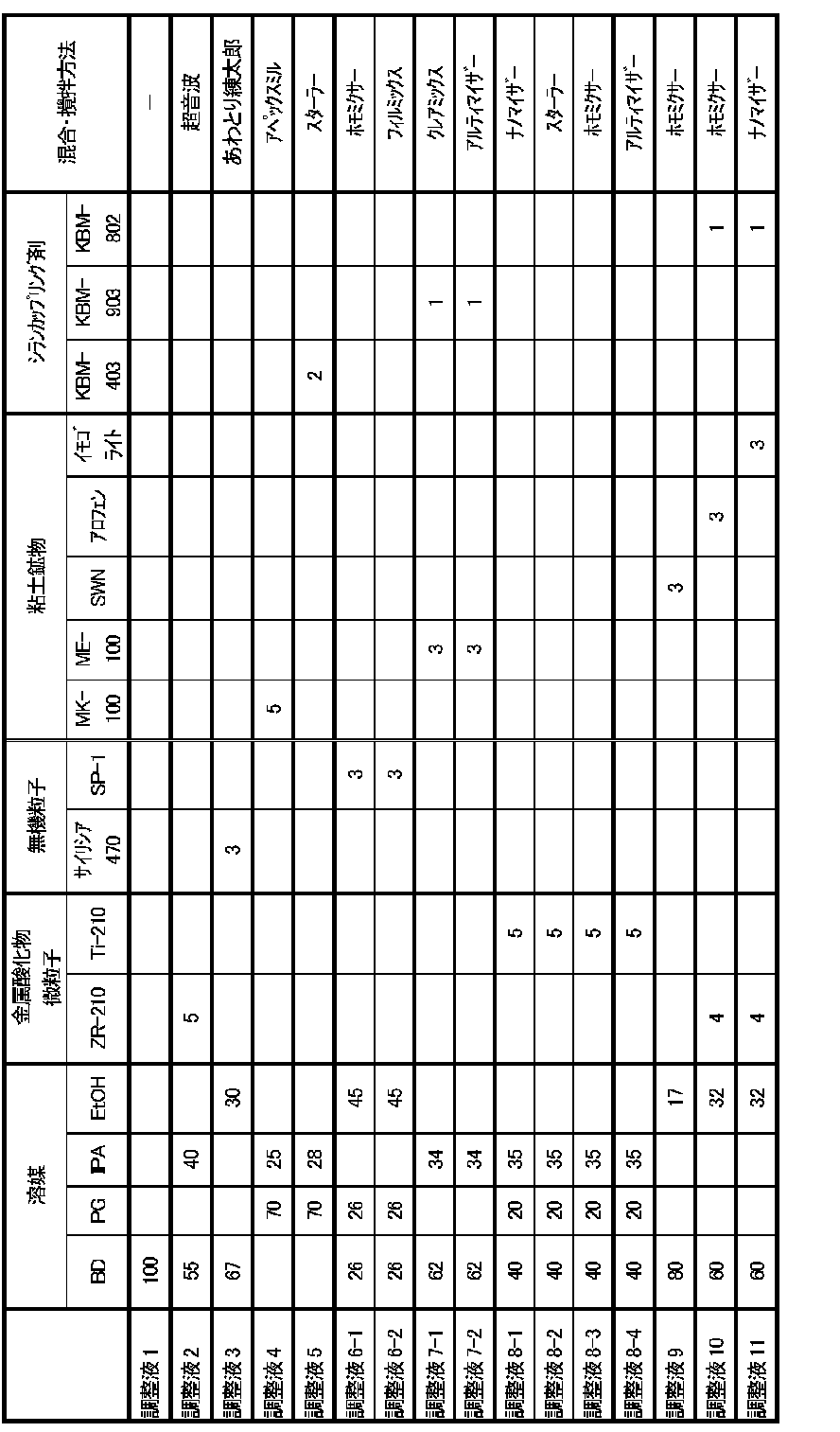
白色顔料と、シラン化合物溶液と、調整液とを、表3に記載の混合比で混合し、塗布液を調製した。
具体的には、白色顔料(A)と上述の方法で調製されたシラン化合物溶液(B)とを混合し、下記表3に示される方法で混合・分散した。そして、上述の方法で調製された調整液(C)に、白色顔料(A)及びシラン化合物溶液(B)の混合液を混合し、下記表3に示される方法で混合・分散した。
表3の略号は以下の成分を表す。
酸化チタン:CR-93 石原産業製
酸化アルミニウム:HD-11 ニッカトー製
酸化亜鉛:ファイネックス50A 堺化学工業製
硫酸バリウム:NFJ-3-1999 山西物産製
窒化ホウ素:AP-100S MARUKA製
表3に示されるように、白色顔料と、シラン化合物溶液と、調整液とを、表3に記載の混合比で全て混合し、ホモミクサーで攪拌して塗布液を調製した。
表3に示されるように、白色顔料と、シラン化合物溶液と、調整液とを、表3に記載の混合比で全て混合し、ナノマイザーで攪拌して塗布液を調製した。
酸化チタン(CR-93:石原産業製)60質量%と、メチルシリコーン樹脂(SCR-1016:信越シリコーン製)40質量%とを、自転・公転式ミキサー(あわとり練太郎:シンキー製)により混合・撹拌し、塗布液を調製した。
酸化チタン(CR-93:石原産業製)60質量%と、フェニルシリコーン樹脂(KER-4000-UV:信越シリコーン製)40質量%とを、自転・公転式ミキサー(あわとり練太郎:シンキー製)により混合・撹拌し、塗布液を調製した。
酸化チタン(CR-93:石原産業製)60質量%と、エポキシ樹脂(W0917:ダイセル製)40質量%を、自転・公転式ミキサー(あわとり練太郎:シンキー製)により混合・撹拌し、塗布液を調製した。
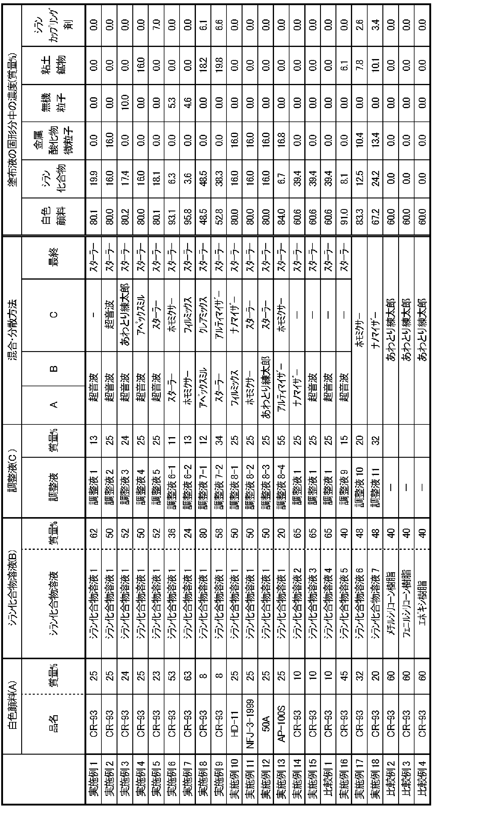
・反射層の評価
各塗布液から得られる反射層について、180℃で1000時間保持後の反射率の低下率、ガラス転移点を測定した。結果を表4に示す。
透明な1mmのガラス板に各実施例及び比較例で調製した塗布液を塗布した。そして、150℃、1時間の熱処理により、硬化させて、厚さ25μmの反射層を有する測定サンプルを作製した。
これらの測定サンプルについて、分光光度計V-670(日本分光株式会社製)で波長500nmの光の反射率を測定し、当該値を初期反射率(反射率A)とした。
続いてこれらのサンプルを、180℃のオーブンに入れ、1000時間保持した。その後、波長500nmの光の反射率(反射率B)を測定した。そして、180℃で1000時間保持後の反射層の反射率の低下率を、以下の式で算出した。
低下率(%)=[(反射率A-反射率B)/反射率A]×100
○:95%以上
△:90%以上、95%未満
透明な1mmのガラス板に各実施例及び比較例で調製した塗布液を塗布した。そして、150℃、1時間の熱処理により、硬化させて、厚さ25μmの反射層を有する測定サンプルを作製した。得られた反射層のガラス転移点を、Q400EM(TAインスツルメンツ社製)により、JIS K7197に基づいてTMA法により、-100℃から10℃/minの割合で昇温して測定した。
さらに、当該塗布液を用いて、以下の方法によりLED装置を作製し、LED装置の耐熱性、アルミ基板との剥離、及びシリコーン材料との剥離を評価した。結果を表4に示す。
金属配線が形成された円形パッケージ(基板)(開口径3mm、底面直径2mm、壁面角度60°)の収容部の中央に、1つの青色LED素子(直方体状;200μm×300μm×100μm)をフリップチップ実装したパッケージを準備した。
前述の実施例及び比較例で調製した塗布液をディスペンサーにより、チップ実装部以外の部分に塗布した。その後、150℃のオーブン中で1時間加熱し、反射層を形成した。
さらに、メチルシリコーン(信越化学工業社製;KER-2500)中に、YAG蛍光体の濃度が10質量%となるように脱泡しながら混合し、波長変換層用組成物を調製した。この波長変換層用組成物を、前述のLED素子の凹部にディスペンサで塗布し、150℃で1時間加熱してLED装置を得た。
各LED装置について、180℃で1000時間の熱処理を行い、試験後の全光束と試験前の全光束とを比較し、LED装置の耐熱性を評価した。各LED装置の全光束値は、20mAの電流値で発光させた状態で、分光放射輝度計(CS-1000A、コニカミノルタセンシング社製)にて測定した。
結果は、以下のように評価した。
○:全光束対初期比(試験後全光束/試験前全光束)が0.95以上である
△:全光束対初期比(試験後全光束/試験前全光束)が0.90以上0.95未満である
×:全光束対初期比(試験後全光束/試験前全光束)が0.90未満である
アルミ基板上に前述の実施例及び比較例で調製した塗布液を塗布し、150℃、1時間の熱処理により、硬化させて、厚さ25μmの反射層を備えた測定サンプルを作製した。この測定サンプルに対して、150℃で30分、-40℃×30分のサイクルを100回行った後の、反射層とアルミ基板との密着性を評価した。
密着性の評価は、反射層にニチバン製セロテープ(登録商標)(24mm)を貼り付け、直ちに剥がす作業を20回繰り返して行った。そして、各回の作業毎に反射層の状態を顕微鏡により観察し、以下のように判断した。
◎:20回作業後も反射層の剥離がみられず、テープの表面に何も付着しなかった。
○:15回作業後は剥離がみられなかったが、20回作業後には剥離がみられた。
△1:10回作業後は剥離がみられなかったが、15回作業後には剥離が発生していた。
△2:15回作業後に剥離は生じなかったが、1回目の作業後に、テープの表面に、白色顔料の粉が僅かに付着した。
×:10回作業時点で反射層の剥離が発生していた。
前述の剥離試験1で、剥離が発生しなかったサンプルの反射層の上から、メチルシリコーン樹脂(信越化学工業社製;KER-2500)を厚み1mmになるように塗布し、150℃、1時間の熱処理により、硬化させた。
このサンプルに対して、150℃で30分、-40℃×30分のサイクルを100回行った後の、反射層とシリコーン樹脂層の密着性を評価した。
密着性の評価は、シリコーン樹脂層にニチバン製セロテープ(登録商標)(24mm)を貼り付け、直ちに剥がす作業を20回繰り返して行った。そして、各回の作業毎にシリコーン層の状態を顕微鏡により観察し、以下のように判断した。
◎:20回作業後もシリコーン層の剥離がみられなかった。
○:15回作業後は剥離がみられなかったが、20回作業後には剥離がみられた。
△:10回作業後は剥離がみられなかったが、15回作業後には剥離がみられた。
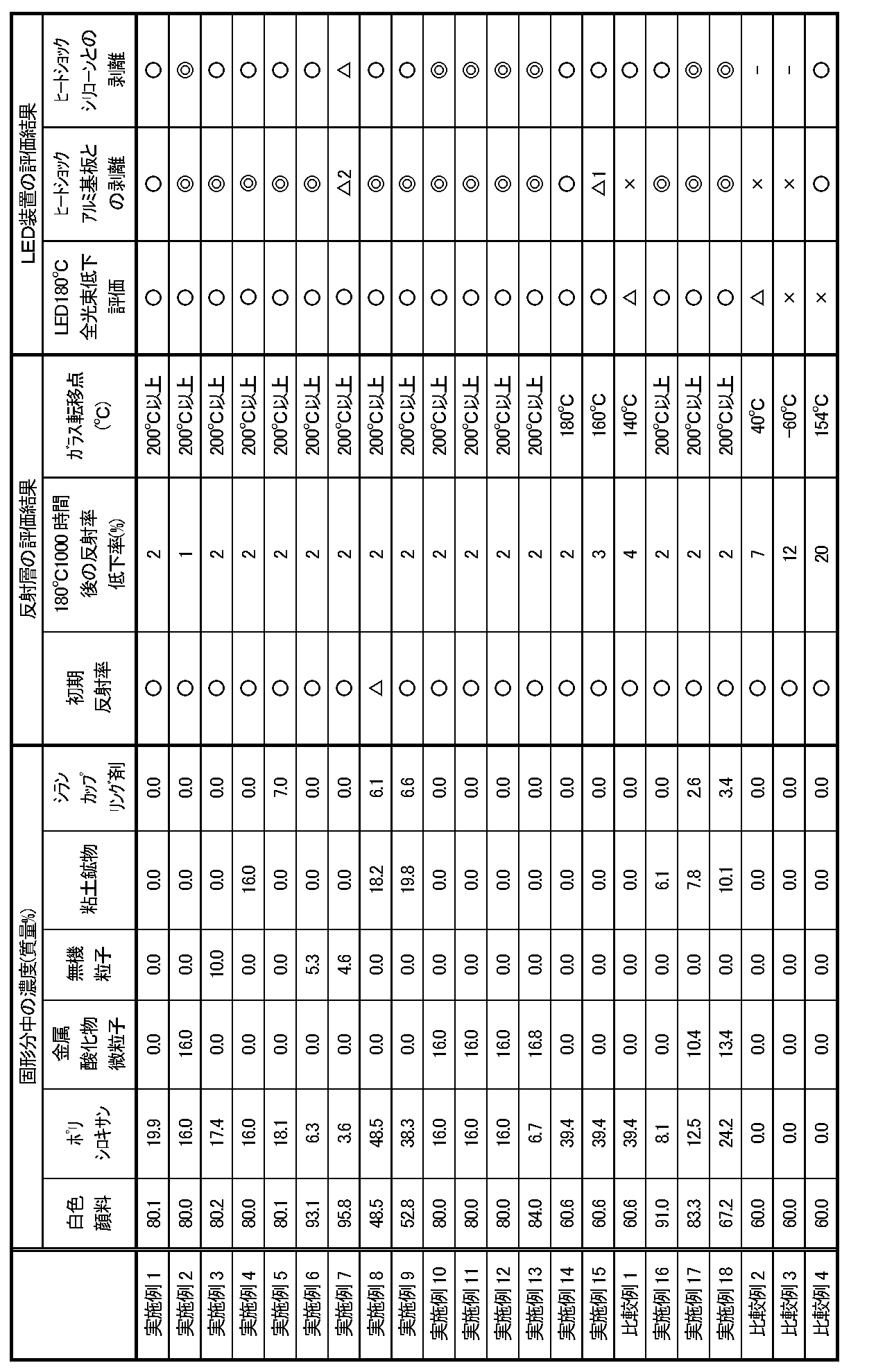
反射層を180℃で1000時間保持した後の反射率の低下が10%以上である場合(比較例3及び4)には、当該反射層を含むLED装置の耐熱性が低くなり、耐熱試験後のLED装置の全光束の低下が許容できなくなることが分かった。
2 LED素子
11、11C、11D、11E 波長変換層
21、21C、21D、21E 反射層
100A、100B、100C、100D、100E LED装置
Claims (13)
- 基板と、前記基板上に配置されたLED素子と、前記基板上の前記LED素子の少なくとも周囲に配置された反射層とを有するLED装置であって、
前記反射層は、白色顔料と、ポリシロキサンとを含有し、
前記反射層を180℃で1000時間保持したときの、前記反射層の波長500nmの光の反射率の低下率が、180℃で保持前の前記反射率に対して10%以下であり、かつ
前記反射層が-70~150℃の範囲にガラス転移点を有さない、LED装置。 - 前記ポリシロキサンに含まれる2官能ケイ素の量が、前記ポリシロキサンに含まれる全ケイ素の量に対して、40質量%以下である、請求項1に記載のLED装置。
- 前記反射層が、金属酸化物微粒子をさらに含有する、請求項1または2に記載のLED装置。
- 前記金属酸化物微粒子は、前記白色顔料よりも平均粒径が小さい、請求項3に記載のLED装置。
- 前記反射層が、無機粒子をさらに含有する、請求項1~4のいずれか一項に記載のLED装置。
- 前記反射層が、粘土鉱物をさらに含有する、請求項1~5のいずれか一項に記載のLED装置。
- 前記粘土鉱物が、層状粘土鉱物、アロフェン、イモゴライトからなる群より選択される少なくとも1種を含有する、請求項6に記載のLED装置。
- 前記反射層が、シランカップリング剤をさらに含有する、請求項1~7のいずれか1項に記載のLED装置。
- 前記白色顔料が、酸化チタン、酸化アルミニウム、硫酸バリウム、酸化亜鉛、窒化ホウ素からなる群から選ばれる少なくとも1種である、請求項1~8のいずれか1項に記載のLED装置。
- 前記反射層に含まれる前記白色顔料の量が、50質量%以上95質量%以下である、請求項1~9のいずれか1項に記載のLED装置。
- 前記反射層は、前記LED素子の配置領域を除く前記基板上に配置されている、請求項1~10のいずれか1項に記載のLED装置。
- 前記反射層は、前記基板と前記LED素子の間に形成されている、請求項1~11のいずれか1項に記載のLED装置。
- LED装置の反射層の製造に用いられる塗布液であって、
前記塗布液は、白色顔料と、ポリシロキサン前駆体とを含有し、
前記塗布液の硬化膜である反射層を、180℃で1000時間保持したときの、前記反射層の波長500nmの光の反射率の低下率が、180℃で保持前の前記反射率に対して10%以下であり、かつ
前記反射層が、-70~150℃の範囲にガラス転移点を有さない、塗布液。
Priority Applications (3)
| Application Number | Priority Date | Filing Date | Title |
|---|---|---|---|
| EP14737661.0A EP2945197A4 (en) | 2013-01-10 | 2014-01-10 | LED DEVICE AND COATING LIQUID FOR THE MANUFACTURE THEREOF |
| US14/759,095 US9708492B2 (en) | 2013-01-10 | 2014-01-10 | LED device and coating liquid used for production of same |
| JP2014556403A JPWO2014109293A1 (ja) | 2013-01-10 | 2014-01-10 | Led装置およびその製造に用いられる塗布液 |
Applications Claiming Priority (2)
| Application Number | Priority Date | Filing Date | Title |
|---|---|---|---|
| JP2013002568 | 2013-01-10 | ||
| JP2013-002568 | 2013-01-10 |
Publications (1)
| Publication Number | Publication Date |
|---|---|
| WO2014109293A1 true WO2014109293A1 (ja) | 2014-07-17 |
Family
ID=51166943
Family Applications (1)
| Application Number | Title | Priority Date | Filing Date |
|---|---|---|---|
| PCT/JP2014/000090 Ceased WO2014109293A1 (ja) | 2013-01-10 | 2014-01-10 | Led装置およびその製造に用いられる塗布液 |
Country Status (4)
| Country | Link |
|---|---|
| US (1) | US9708492B2 (ja) |
| EP (1) | EP2945197A4 (ja) |
| JP (1) | JPWO2014109293A1 (ja) |
| WO (1) | WO2014109293A1 (ja) |
Cited By (6)
| Publication number | Priority date | Publication date | Assignee | Title |
|---|---|---|---|---|
| JP2016042449A (ja) * | 2014-08-19 | 2016-03-31 | 株式会社ジャパンディスプレイ | 表示装置 |
| WO2016071456A1 (de) * | 2014-11-07 | 2016-05-12 | Osram Opto Semiconductors Gmbh | Optoelektronisches bauelement und verfahren zum herstellen des optoelektronischen bauelements |
| JP2017145312A (ja) * | 2016-02-17 | 2017-08-24 | 日本タングステン株式会社 | 紫外線反射膜形成用塗料および紫外線反射膜 |
| JP2017163053A (ja) * | 2016-03-10 | 2017-09-14 | パナソニックIpマネジメント株式会社 | Ledモジュール |
| JP7227004B2 (ja) | 2015-12-15 | 2023-02-21 | マテリオン コーポレイション | 改良された波長変換デバイス |
| JP7795672B1 (ja) * | 2025-02-21 | 2026-01-07 | 青島上雅家居用品股▲ふん▼有限公司 | マスターバッチ、放射冷却繊維、放射冷却多層織物及びその応用 |
Families Citing this family (13)
| Publication number | Priority date | Publication date | Assignee | Title |
|---|---|---|---|---|
| EP2977682B1 (en) * | 2014-07-25 | 2018-05-30 | Electrolux Appliances Aktiebolag | Oven door, oven comprising an oven door and method for displaying information at an oven door |
| WO2016017592A1 (ja) * | 2014-07-28 | 2016-02-04 | 住友化学株式会社 | シリコーン系封止材組成物及び半導体発光装置 |
| KR102170218B1 (ko) * | 2014-08-05 | 2020-10-26 | 엘지이노텍 주식회사 | 발광소자 패키지 |
| US10326066B2 (en) * | 2015-10-29 | 2019-06-18 | Kyocera Corporation | Light emitting element-mounting substrate and light emitting apparatus |
| US10193031B2 (en) * | 2016-03-11 | 2019-01-29 | Rohinni, LLC | Method for applying phosphor to light emitting diodes and apparatus thereof |
| DE102016106494A1 (de) * | 2016-04-08 | 2017-10-12 | Osram Opto Semiconductors Gmbh | Optoelektronisches bauelement und verfahren zum herstellen eines optoelektronischen bauelements |
| DE102016109352B4 (de) | 2016-05-20 | 2022-03-24 | Infineon Technologies Ag | Chipgehäuse und verfahren zum bilden eines chipgehäuses |
| US10672678B2 (en) * | 2016-05-20 | 2020-06-02 | Infineon Technologies Ag | Method for forming a chip package with compounds to improve the durability and performance of metal contact structures in the chip package |
| US10193043B2 (en) * | 2016-07-28 | 2019-01-29 | Lumileds Llc | Light emitting device package with reflective side coating |
| DE102016113969A1 (de) * | 2016-07-28 | 2018-02-01 | Osram Opto Semiconductors Gmbh | Strahlungsemittierender Halbleiterchip, Verfahren zur Herstellung einer Vielzahl strahlungsemittierender Halbleiterchips, strahlungsemittierendes Bauelement und Verfahren zur Herstellung eines strahlungsemittierenden Bauelements |
| US10672960B2 (en) | 2017-10-19 | 2020-06-02 | Lumileds Llc | Light emitting device package with a coating layer |
| DE102018106465B4 (de) * | 2018-03-20 | 2024-03-21 | OSRAM Opto Semiconductors Gesellschaft mit beschränkter Haftung | Optoelektronisches Bauteil |
| KR102716558B1 (ko) * | 2019-04-30 | 2024-10-15 | 엘지전자 주식회사 | 반도체 발광소자를 이용한 디스플레이 장치 |
Citations (7)
| Publication number | Priority date | Publication date | Assignee | Title |
|---|---|---|---|---|
| JP2005136379A (ja) | 2003-10-08 | 2005-05-26 | Nichia Chem Ind Ltd | 半導体装置 |
| JP2005200546A (ja) * | 2004-01-15 | 2005-07-28 | Shin Etsu Chem Co Ltd | シリコーンレジン組成物及びそれを用いた被覆物品 |
| JP2010205954A (ja) * | 2009-03-04 | 2010-09-16 | Micro Coatec Kk | Led照明構造体 |
| JP2011023621A (ja) | 2009-07-17 | 2011-02-03 | Sharp Corp | 発光装置 |
| JP2011054902A (ja) * | 2009-09-04 | 2011-03-17 | Shin-Etsu Chemical Co Ltd | 光半導体ケース形成用白色熱硬化性シリコーン樹脂組成物及び光半導体ケース |
| JP2012124358A (ja) * | 2010-12-09 | 2012-06-28 | Citizen Holdings Co Ltd | 半導体発光装置及びその製造方法 |
| JP2012138536A (ja) * | 2010-12-28 | 2012-07-19 | Konica Minolta Advanced Layers Inc | 発光装置の製造方法 |
Family Cites Families (10)
| Publication number | Priority date | Publication date | Assignee | Title |
|---|---|---|---|---|
| JP4623322B2 (ja) * | 2007-12-26 | 2011-02-02 | 信越化学工業株式会社 | 光半導体ケース形成用白色熱硬化性シリコーン樹脂組成物並びに光半導体ケース及びその成形方法 |
| JP2010106243A (ja) * | 2008-09-30 | 2010-05-13 | Shin-Etsu Chemical Co Ltd | 光半導体装置用シリコーン樹脂組成物 |
| JP5108825B2 (ja) * | 2009-04-24 | 2012-12-26 | 信越化学工業株式会社 | 光半導体装置用シリコーン樹脂組成物及び光半導体装置 |
| EP2448026A4 (en) * | 2009-06-26 | 2013-08-14 | Asahi Rubber Inc | MATERIAL FOR REFLEXING WHITE COLOR AND METHOD OF MANUFACTURING THEREOF |
| WO2011118109A1 (ja) * | 2010-03-23 | 2011-09-29 | 株式会社朝日ラバー | 可撓性反射基材、その製造方法及びその反射基材に用いる原材料組成物 |
| WO2011125753A1 (ja) * | 2010-04-02 | 2011-10-13 | 株式会社カネカ | 硬化性樹脂組成物、硬化性樹脂組成物タブレット、成形体、半導体のパッケージ、半導体部品及び発光ダイオード |
| KR20120139594A (ko) * | 2011-06-16 | 2012-12-27 | 닛토덴코 가부시키가이샤 | 실리콘 수지 조성물, 봉지층, 리플렉터 및 광반도체 장치 |
| US9793456B2 (en) * | 2011-09-30 | 2017-10-17 | Kaneka Corporation | Molded resin body for surface-mounted light-emitting device, manufacturing method thereof, and surface-mounted light-emitting device |
| JP5814175B2 (ja) * | 2012-04-16 | 2015-11-17 | 信越化学工業株式会社 | Ledのリフレクター用熱硬化性シリコーン樹脂組成物並びにこれを用いたled用リフレクター及び光半導体装置 |
| US9593240B2 (en) * | 2012-11-13 | 2017-03-14 | Jnc Corporation | Thermosetting resin composition |
-
2014
- 2014-01-10 WO PCT/JP2014/000090 patent/WO2014109293A1/ja not_active Ceased
- 2014-01-10 US US14/759,095 patent/US9708492B2/en not_active Expired - Fee Related
- 2014-01-10 EP EP14737661.0A patent/EP2945197A4/en not_active Withdrawn
- 2014-01-10 JP JP2014556403A patent/JPWO2014109293A1/ja active Pending
Patent Citations (7)
| Publication number | Priority date | Publication date | Assignee | Title |
|---|---|---|---|---|
| JP2005136379A (ja) | 2003-10-08 | 2005-05-26 | Nichia Chem Ind Ltd | 半導体装置 |
| JP2005200546A (ja) * | 2004-01-15 | 2005-07-28 | Shin Etsu Chem Co Ltd | シリコーンレジン組成物及びそれを用いた被覆物品 |
| JP2010205954A (ja) * | 2009-03-04 | 2010-09-16 | Micro Coatec Kk | Led照明構造体 |
| JP2011023621A (ja) | 2009-07-17 | 2011-02-03 | Sharp Corp | 発光装置 |
| JP2011054902A (ja) * | 2009-09-04 | 2011-03-17 | Shin-Etsu Chemical Co Ltd | 光半導体ケース形成用白色熱硬化性シリコーン樹脂組成物及び光半導体ケース |
| JP2012124358A (ja) * | 2010-12-09 | 2012-06-28 | Citizen Holdings Co Ltd | 半導体発光装置及びその製造方法 |
| JP2012138536A (ja) * | 2010-12-28 | 2012-07-19 | Konica Minolta Advanced Layers Inc | 発光装置の製造方法 |
Non-Patent Citations (2)
| Title |
|---|
| "Optimum Application Technique for Coupling Agents", NATIONAL INSTITUTE OF SCIENCE AND TECHNOLOGY POLICY |
| See also references of EP2945197A4 |
Cited By (6)
| Publication number | Priority date | Publication date | Assignee | Title |
|---|---|---|---|---|
| JP2016042449A (ja) * | 2014-08-19 | 2016-03-31 | 株式会社ジャパンディスプレイ | 表示装置 |
| WO2016071456A1 (de) * | 2014-11-07 | 2016-05-12 | Osram Opto Semiconductors Gmbh | Optoelektronisches bauelement und verfahren zum herstellen des optoelektronischen bauelements |
| JP7227004B2 (ja) | 2015-12-15 | 2023-02-21 | マテリオン コーポレイション | 改良された波長変換デバイス |
| JP2017145312A (ja) * | 2016-02-17 | 2017-08-24 | 日本タングステン株式会社 | 紫外線反射膜形成用塗料および紫外線反射膜 |
| JP2017163053A (ja) * | 2016-03-10 | 2017-09-14 | パナソニックIpマネジメント株式会社 | Ledモジュール |
| JP7795672B1 (ja) * | 2025-02-21 | 2026-01-07 | 青島上雅家居用品股▲ふん▼有限公司 | マスターバッチ、放射冷却繊維、放射冷却多層織物及びその応用 |
Also Published As
| Publication number | Publication date |
|---|---|
| EP2945197A4 (en) | 2016-08-03 |
| EP2945197A1 (en) | 2015-11-18 |
| JPWO2014109293A1 (ja) | 2017-01-19 |
| US20150353740A1 (en) | 2015-12-10 |
| US9708492B2 (en) | 2017-07-18 |
Similar Documents
| Publication | Publication Date | Title |
|---|---|---|
| WO2014109293A1 (ja) | Led装置およびその製造に用いられる塗布液 | |
| JP5742839B2 (ja) | 発光装置及びその製造方法 | |
| WO2014103326A1 (ja) | 塗布液、及びその硬化物からなる反射層を備えるled装置 | |
| EP2940743A1 (en) | Light emitting device | |
| WO2013099193A1 (ja) | Led装置用封止剤、led装置、及びled装置の製造方法 | |
| WO2013180259A1 (ja) | 発光装置用封止材、及びこれを用いた発光装置、並びに発光装置の製造方法 | |
| JP5910340B2 (ja) | Led装置、及びその製造方法 | |
| WO2015011925A1 (ja) | Led装置の製造方法 | |
| JP2014138081A (ja) | 発光装置、波長変換・光拡散素子及びそれらの製造方法、光拡散セラミック層形成用組成物 | |
| JPWO2013121903A1 (ja) | 波長変換素子及びその製造方法、発光装置及びその製造方法 | |
| EP2940744A1 (en) | Phosphor dispersion, led device and method for manufacturing same | |
| JP2016154179A (ja) | 発光装置、及びその製造方法 | |
| JP2014127495A (ja) | Led装置、及びその製造方法 | |
| JP2014019844A (ja) | 蛍光体分散液及びled装置の製造方法 | |
| WO2013180258A1 (ja) | 発光装置用封止材、及びこれを用いた発光装置、並びに発光装置の製造方法 | |
| JP5747994B2 (ja) | 波長変換素子及びその製造方法、発光装置及びその製造方法 | |
| JP2016181535A (ja) | 発光装置、および発光装置製造用の塗布液 | |
| JPWO2014091762A1 (ja) | Led装置用封止剤、及びこれを用いたled装置 | |
| JP2014041955A (ja) | Led装置、及びその製造方法 | |
| JP5729327B2 (ja) | Led装置の製造方法 | |
| WO2013105514A1 (ja) | Led装置 | |
| JP2014160713A (ja) | Led装置の製造方法 | |
| WO2016047745A1 (ja) | 塗布液、それを用いたled装置の製造方法およびled装置 | |
| JPWO2016024604A1 (ja) | 無機微粒子含有ポリシルセスキオキサン組成物およびその製造方法、ならびに発光装置およびその製造方法 | |
| WO2015049865A1 (ja) | 発光素子用封止剤及びled装置 |
Legal Events
| Date | Code | Title | Description |
|---|---|---|---|
| 121 | Ep: the epo has been informed by wipo that ep was designated in this application |
Ref document number: 14737661 Country of ref document: EP Kind code of ref document: A1 |
|
| ENP | Entry into the national phase |
Ref document number: 2014556403 Country of ref document: JP Kind code of ref document: A |
|
| REEP | Request for entry into the european phase |
Ref document number: 2014737661 Country of ref document: EP |
|
| WWE | Wipo information: entry into national phase |
Ref document number: 2014737661 Country of ref document: EP |
|
| WWE | Wipo information: entry into national phase |
Ref document number: 14759095 Country of ref document: US |
|
| NENP | Non-entry into the national phase |
Ref country code: DE |