WO2014109601A1 - Procédé d'obtention de données de motif de panneau d'affichage associées à un système d'affichage par superposition, et système d'affichage par superposition - Google Patents
Procédé d'obtention de données de motif de panneau d'affichage associées à un système d'affichage par superposition, et système d'affichage par superposition Download PDFInfo
- Publication number
- WO2014109601A1 WO2014109601A1 PCT/KR2014/000327 KR2014000327W WO2014109601A1 WO 2014109601 A1 WO2014109601 A1 WO 2014109601A1 KR 2014000327 W KR2014000327 W KR 2014000327W WO 2014109601 A1 WO2014109601 A1 WO 2014109601A1
- Authority
- WO
- WIPO (PCT)
- Prior art keywords
- display panel
- display
- pixel
- angle
- pixels
- Prior art date
- Legal status (The legal status is an assumption and is not a legal conclusion. Google has not performed a legal analysis and makes no representation as to the accuracy of the status listed.)
- Ceased
Links
Images


Classifications
-
- G—PHYSICS
- G09—EDUCATION; CRYPTOGRAPHY; DISPLAY; ADVERTISING; SEALS
- G09G—ARRANGEMENTS OR CIRCUITS FOR CONTROL OF INDICATING DEVICES USING STATIC MEANS TO PRESENT VARIABLE INFORMATION
- G09G3/00—Control arrangements or circuits, of interest only in connection with visual indicators other than cathode-ray tubes
- G09G3/006—Electronic inspection or testing of displays and display drivers, e.g. of LED or LCD displays
-
- H—ELECTRICITY
- H10—SEMICONDUCTOR DEVICES; ELECTRIC SOLID-STATE DEVICES NOT OTHERWISE PROVIDED FOR
- H10K—ORGANIC ELECTRIC SOLID-STATE DEVICES
- H10K71/00—Manufacture or treatment specially adapted for the organic devices covered by this subclass
- H10K71/70—Testing, e.g. accelerated lifetime tests
-
- G—PHYSICS
- G09—EDUCATION; CRYPTOGRAPHY; DISPLAY; ADVERTISING; SEALS
- G09G—ARRANGEMENTS OR CIRCUITS FOR CONTROL OF INDICATING DEVICES USING STATIC MEANS TO PRESENT VARIABLE INFORMATION
- G09G2300/00—Aspects of the constitution of display devices
- G09G2300/02—Composition of display devices
- G09G2300/023—Display panel composed of stacked panels
Definitions
- the present invention relates to a display device.
- a display device In particular, in the case where two different display panels are superimposed and displayed to overlap each other, minimizing the occurrence of moire caused when the two display panels overlap each other.
- LCDs Liquid crystal displays
- LCDs are widely used as various display devices such as displays of televisions, desktop computers and notebook computers, and displays for mobile phones.
- LCD Since LCD is not a self-luminous display device that generates light by itself, an auxiliary light emitting device called a backlight is used on the back of the liquid crystal panel. As such backlight, a cold cathode fluorescent lamp (CCFL) is mainly used.
- CCFL cold cathode fluorescent lamp
- various types of display devices are used for the instrument panel of a vehicle such as a vehicle to provide a driver with various information such as a speedometer and navigation, and the amount of information provided is gradually increasing.
- a limitation in size and as an alternative to this, an attempt has been made to display overlapping information by overlapping two or more display devices.
- a transparent display device such as an inorganic EL display device is superimposed in front of the liquid crystal display device.
- positions and displays an overlap is also shown (refer patent document 1).
- Patent Document 2 there is a technique described in Patent Document 2 as a moiré prevention measure in the case where two display apparatuses are spaced apart from each other at regular intervals.
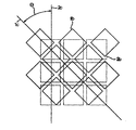
- Patent Document 1 is a plan view illustrating a pixel array pattern of two display devices overlapped by Patent Document 2.
- the light transmissive first display device 1 in which a plurality of pixels 1b are arranged in one direction and a plurality of pixels 2b are arranged in one direction in a stripe shape.
- the direction in which the pixels 1b of the first display device 1 are arranged in the direction in which both display devices overlap are suppressed by arranging both display devices such that the angle ⁇ formed by the array direction 2c of the pixels 2b of the second display device is shifted from each other within a range of 20 degrees to 70 degrees.
- Patent Literature 2 suppresses the occurrence of moiré by adjusting the placement angle when the display device is actually installed on the two display devices that are already manufactured. Therefore, the arrangement angle of both display devices is adjusted every time the display device is installed. There is a hassle to do.
- the display device when the angle (theta) formed between the arrangement direction 1c of the pixel 1b of the 1st display apparatus 1, and the arrangement direction 2c of the pixel 2b of a 2nd display apparatus is 45 degree
- the display device has a plurality of pixels arranged in a matrix shape, and thus the display device is generally formed in a rectangular shape such as a rectangle or a square, and two display devices forming such a rectangular shape If you place them at a 45-degree angle to each other, there is a problem such as that the arrangement space becomes large.
- Patent Document 1 Japanese Patent Application Laid-Open No. 2005-231530 (published Sep. 2, 2005)
- Patent Document 2 Japanese Patent Application Laid-Open No. 2007-233118 (published Sep. 13, 2007)
- the present invention is to solve the problems of the prior art as described above, to minimize the occurrence of moiré in the superimposed display system to display the superimposed image by placing two display devices consisting of the first display panel and the second display panel overlapping It is an object of the present invention to provide a method for obtaining pixel design data of a second display panel.
- Another object of the present invention is to provide a second display panel manufactured by the pixel design data and an overlapping display system using the second display panel.
- the display panel design data acquisition to obtain the design data of the display panel minimized the generation of moiré in the superimposed display system that overlaps the first display panel and the second display panel to display the superimposed image A method comprising: preparing a first display panel in which a plurality of pixels having a predetermined shape are arranged in a matrix and a second display panel for test having a plurality of pixels having the same shape and arrangement as the first display panel; The first display panel and the test second display panel are overlapped with each other, and one of the first display panel and the test second display panel is fixed and the other display panel is rotated to minimize moiré generation. Confirming a point at which is to be made, and the first display panel and the test second display panel at a point where the moiré generation is minimized. And a step of obtaining the pixel data for the display panel from its design angle.
- the superimposed display system of the present invention is an superimposed display system in which a first display panel and a second display panel are superimposed to display an superimposed image, wherein any one of the first display panel and the second display panel is displayed.
- the superimposed display system of the present invention is an superimposed display system in which a first display panel and a second display panel are superimposed to display an superimposed image, wherein any one of the first display panel and the second display panel is displayed.
- the shape of a pixel is made into the shape of the cut surface which cut
- the pixel design data of the second display panel which can minimize the generation of moiré, can be simplified in the superimposed display system in which two display devices including the first display panel and the second display panel are superimposed to display the superimposed image. It can be obtained by the method.
- a superimposed display system capable of superimposed display with minimum moiré generation can be provided by constructing an superimposed display system using a second display panel manufactured by the pixel design data.
- 1 is a plan view illustrating a pixel array pattern of two display devices overlapping each other according to the related art.
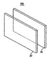
- FIG. 2 is a view schematically showing a usage of the superimposed display system according to the present invention.
- FIG. 3 is an electron microscope photograph of a part of a pixel area of a transparent LCD panel applied to an overlapping display system according to a preferred embodiment of the present invention.
- Fig. 4 is an electron microscope photograph of a part of the pixel region of the transparent OLED panel applied to the superimposed display system of the preferred embodiment of the present invention.
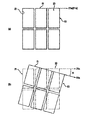
- FIG. 5 is a diagram schematically illustrating a method of obtaining pixel design data of a second display panel according to a preferred embodiment of the present invention.
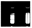
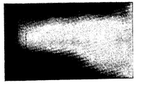
- FIG. 6 is a photograph showing a state of moiré patterns occurring in the superimposed display system.
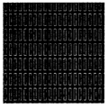
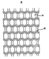
- FIG. 7 is a view showing the shape and arrangement of each pixel of a pixel region of a second display panel manufactured using pixel design data of a second display panel of a preferred embodiment of the present invention.
- FIG. 8 is a diagram illustrating an example of a shape and an arrangement of pixels using pixel design data of a second display panel according to a preferred embodiment of the present invention.
- FIG. 9 is a diagram showing an example of an arrangement of auxiliary electrodes using pixel design data of a second display panel according to a preferred embodiment of the present invention.
- FIG. 2 is a view schematically showing the usage of the superimposed display system 100 according to the present invention.
- two display panels including the first display panel 20 and the second display panel 30 are overlapped with each other, and the first display panel is overlapped with each other.
- An air layer is interposed between the 20 and the second display panel 30.
- the overlapping display system of the present invention is not limited to the first and second display panels overlapping each other via an air layer, and also includes a case in which the first and second display panels overlap each other.
- the first display panel 20 may be, for example, an LCD, a transparent LCD, an organic light emitting display (OLED) or a transparent OLED
- the second display panel 30 may be an OLED or a transparent OLED.
- the superimposed display system 100 When the superimposed display system 100 is used as an image display device for displaying an image of a television, a computer or a mobile phone, for example, the first display panel 20 displays an image such as an LCD or a transparent LCD.
- the display device which displays directly on a panel can be used, and the 2nd display panel 30 can be set as the backlight of the 1st display panel 20.
- both the first display panel 20 and the second display panel 30 can be used as a display device that displays an image directly.
- the first display panel 20 is preferably a transparent LCD or a transparent OLED so that an image of the second display panel 30 disposed behind the display system 100 can be observed from the front.
- the display panel of the two display panels 20 and 30 that is closer to the observer is displayed on the first display panel 20 and the farther side.
- the panel will be described as the second display panel 30.
- the first display panel 20 has a structure in which a plurality of pixels are arranged in a matrix shape, and each pixel has a shape and an arrangement as shown in FIG. 4, for example.
- the second display panel 30 also has a structure in which a plurality of pixels are arranged in a matrix shape, and each pixel has a shape and an arrangement as shown in FIG. 7, for example, thereby achieving the problem of the present invention.
- Patent Document 2 which is a prior art, arranges two display panels having the same horizontal axis direction of pixels in order to minimize the moiré phenomenon that occurs when two display apparatuses are superimposed to display an overlapped image.
- the present invention does not adjust the arrangement direction of the two display panels, but the shape of the pixels of the first display panel and the second display panel, The arrangement of the pixel electrodes and the arrangement of the pixel electrodes are different from each other to minimize the occurrence of moiré phenomenon.
- test second display panel 50 having the same shape and arrangement as that of each pixel 21 of the first display panel 20 is prepared.
- the test second display panel 50 is a display panel in which the shape and arrangement of each pixel 51 constituting the display panel are the same as the shape and arrangement of each pixel 21 of the first display panel 20. To this end, a test second display panel 50 having the same shape and arrangement as that of the first display panel 20 may be manufactured using the design data of the first display panel 20. . In this case, the shape and arrangement of the pixels 21 of the first display panel 20 and the pixels 51 of the second display panel 50 for testing may be shaped and arranged as shown in FIG. 4. have.
- each pixel of the first display panel 20 and the test second display panel 50 is the same, for example, the shape of each pixel 21 of the first display panel 20 is shown in FIG. 4.
- the shape of each pixel 51 of the test second display panel 50 is the same as the rectangular shape, and the shapes of the pixels of both display panels 20 and 50 coincide with each other.
- the arrangement of the pixels 21 of the first display panel 20 and the arrangement of the pixels 51 of the test second display panel 50 are the same, for example, the first display panel 20.
- the horizontal axis directions of the pixels of each of the second display panels 50 for testing are arranged to coincide with each other in the longitudinal direction and the width direction of the display panel as shown in FIG. 4.
- the size of each pixel (such as pixel pitch and width) and the spacing between the plurality of pixels of the display panels 20 and 50 must also be the same.
- the horizontal axis direction 21a of the pixels of the first display panel 20 and the horizontal axis direction 51a of the pixels of the test second display panel 50 coincide with each other.
- the first display panel 20 and the test second display panel 50 are operated together to observe the display image of the first display panel 20.
- the coupling between the two display panels 20 and 50 may be performed so that the two display panels 20 and 50 are in contact with each other, as well as the coupling between the air layers as shown in FIG. 2.
- the observation of the moiré phenomenon may be based on visual observation, but for more accurate observation, it is preferable to use a known moiré inspection device such as a video meter or a 2D camera.
- the first display panel 20 is rotated while the first display panel 20 is fixed so that the angle between the display panels 20 and 50 can be changed.
- the first display panel 20 is gradually changed while the angle R between the horizontal axis direction 21a of the pixel of the first display panel 20 and the horizontal axis direction 51a of the pixel of the second display panel 50 for testing is gradually changed.
- an angle R having the least occurrence of moiré phenomenon is obtained, and the pixel design data for the second display panel 30 is obtained from this angle R.
- the observation of the moiré phenomenon at this time may also be based on visual observation, but for more accurate observation, it is preferable to use a known moiré inspection apparatus such as a video meter or a 2D camera.
- the second display panel 30 has a horizontal axis direction 21a of the pixels of the first display panel 20 in which the moiré phenomenon is minimal and a horizontal axis of the pixels of the test second display panel 50.
- the angle R between the directions 51a is applied to determine the shape of the pixel, the shape of the auxiliary electrode, and the like, thereby manufacturing the second display panel 30.
- the shape of the pixel of the second display panel 30 is illustrated in FIGS. 8A to 8D. It is set as the shape which combined one or these mutually. However, the arrangement of the plurality of pixels of the second display panel 30 is not changed, and the arrangement is the same as that of the first display panel 20.
- each pixel of the second display panel 30 is a cut surface obtained by cutting a part of two corner portions facing each other out of four corner portions of a rectangle, and in this case, the horizontal axis direction ( The horizontal axis direction 21a of the pixel of the first display panel 20 and the pixel of the test second display panel 50 for which the occurrence of the moiré phenomenon is minimized at an angle b between 21a and the cut surface direction 31a. It is set to the same angle as the angle R between the horizontal axis directions 51a.
- each pixel of the second display panel 30 is a cut surface obtained by cutting a part of four rectangular corners, where the horizontal axis direction 21a and the cut surface direction ( The horizontal axis direction 21a of the pixels of the first display panel 20 and the horizontal axis direction 51a of the pixels of the test second display panel 50 for which the occurrence of the moire phenomenon is minimized at an angle b between 31a). It is set as the same angle as the angle R between ().
- each pixel of the second display panel 30 is a cut surface obtained by cutting the entire four corners of the rectangle.
- the horizontal axis direction 21a and the cut surface direction ( The horizontal axis direction 21a of the pixels of the first display panel 20 and the horizontal axis direction 51a of the pixels of the test second display panel 50 for which the occurrence of the moire phenomenon is minimized at an angle b between 31a). It is set as the same angle as the angle R between ().
- the first display having the minimum occurrence of the moiré phenomenon at the angle b between the horizontal axis direction 21a and the vertical axis direction 31a of the pixel at this time. It is set as the angle equal to the angle R between the horizontal axis direction 21a of the pixel of the panel 20, and the horizontal axis direction 51a of the pixel of the 2nd display panel 50 for a test.
- the shape of the auxiliary electrode 32 may be appropriately changed in accordance with the shape of the pixel of the second display panel 30.
- the shape of the auxiliary electrode 32 is substantially linear in consideration of convenience in manufacturing process and the like.
- the shape of the pixel of the second display panel 30 is superimposed with the first display panel 20 in the present superimposed display system 100 to display the superimposed image.
- the shape of the auxiliary electrode 32 also corresponds to the shape of the pixel as shown in FIG. 9.
- the array shape of the auxiliary electrodes 32 of the second display panel 30 has a wavy shape as shown in FIGS. 7 and 9, in which the auxiliary direction of the horizontal axis direction 21a and the wavy pattern of each pixel is formed.
- the horizontal axis direction 21a of the pixel of the first display panel 20 and the second display panel 50 for testing are minimized by the angle b between the array direction 32a of the electrode 32. It is preferable to set the same angle as the angle R between the horizontal axis directions 51a of the pixels.
- FIG. 7 shows an example of the shape and arrangement of each pixel in the pixel region of the second display panel fabricated using the pixel design data of the second display panel of the preferred embodiment of the present invention.
- the present inventors use the first display panel 20 as a transparent LCD, and the test second display panel 50 as a transparent OLED.
- the pixel design data is obtained, and the second display panel 30 is manufactured by using the design data, and the first display panel 20 made of a transparent LCD and the second display panel 30 made of a transparent OLED are overlapped to each other.
- the degree of occurrence of the moiré phenomenon of the superimposed display system 100 was measured, and the results are shown in Table 1 below.
- the experiment was carried out with a sample (sample 1) having a pitch of 60 ⁇ m, a sample having a pitch of 75 ⁇ m (sample 2) and a 150 ⁇ m, respectively, of the plurality of pixels of the first display panel 20 and the test second display panel 50.
- a sample (sample 1) having a pitch of 60 ⁇ m, a sample having a pitch of 75 ⁇ m (sample 2) and a 150 ⁇ m, respectively, of the plurality of pixels of the first display panel 20 and the test second display panel 50.
- One sample (sample 3) was produced, and the horizontal axis direction 21a of the pixels of the first display panel 20 in which the moiré phenomenon was minimized by the method described above for each of the samples 1, 2, and 3, and for the test
- the angle R between the horizontal axis directions 51a of the pixels of the second display panel 50 was measured.
- the angle R between the first display panel 20 and the test second display panel 50 was approximately 8 °, and 24. In the range from ° to 60 °, the generation of moire was the least, and in Sample 2 where the pixel pitch was 75 ⁇ m, the angle R between the first display panel 20 and the test second display panel 50 was observed. In the case of approximately 11 ° and in the range of 15 ° to 62 °, the generation of moire was the least. In the sample 3 having the pixel pitch of 150 ⁇ m, the first display panel 20 and the second display panel for test were shown. The incidence of moiré was the least in the range (R) between (50) in the range of approximately 8-13 ° and in the range of 25 ° -65 °.
- a second display panel 30 having an angle equal to this angle R is fabricated, and a superimposed display system 100 in which the first display panel 20 and the second display panel 30 are superimposed and manufactured is fabricated.
- the degree of moiré generation was measured, and the shape of each pixel 31 of the second display panel 30 and the shape and arrangement of the auxiliary electrode 32 were as shown in FIG. 7.
- the angle between the horizontal axis direction of each pixel of the first display panel 20 and the horizontal axis direction of each pixel of the second display panel 50 for testing is in a range of 24 ° to 60 °. It is preferable.
- the shape of the pixels of the second display panel 30 for minimizing the moiré generation in the superimposed display system 100 in which the first display panel 20 and the second display panel 30 are overlapped to display the superimposed images Is a cut surface obtained by cutting at least one portion of at least four corner portions of a rectangle, wherein the angle b between the horizontal axis direction 21a of the pixel and the cut surface direction 31a is in a range of 24 ° or more and 60 ° or less.
- the shapes of the pixels of the second display panel 30 may be formed in a quadrangular shape where the angles of the neighboring cabinets are different from each other and the angles of the cabinets facing each other are the same. In this case, the horizontal axis direction 21a and the vertical axis of the pixels It is preferable to make angle b between directions 31a into the range of 24 degrees or more and 60 degrees or less.
- the arrangement of the auxiliary electrodes 32 of the second display panel 30 has a shape corresponding to the arrangement of the pixels, and the horizontal axis direction 21a of each pixel and the arrangement direction 32a of the auxiliary electrode 32. It is preferable to make angle b between them into the range of 24 degrees or more and 60 degrees or less.
- the test second display panel 50 having the same pixel shape and arrangement as the first display panel 20 is directly manufactured, and both display panels 20 and 50 are overlapped and arranged. Fixing the first display panel 20 and rotating the test second display panel 50 while the moire phenomenon is minimized, the horizontal axis direction 21a of the pixels of the first display panel 20 and the test agent Although the angle R between the horizontal axis direction 51a of the pixel of the display panel 50 is directly measured, the present invention is not limited thereto.
- the measurement may be performed by, for example, a simulation using a computer system equipped with a simulation program.
- a virtual first display panel is formed by inputting pixel information of a display panel including a shape and an arrangement of pixels of the first display panel 20 into a computer system, and forming a virtual first display.
- the virtual test second display panel After forming the virtual test second display panel having the same pixel information as the pixel information of the display panel including the shape and arrangement of the pixels of the panel, the virtual first display panel and the virtual test second display panel are superimposed. To form a virtual superimposed display system in the same manner as in the above embodiment.
- the virtual first display panel of the virtual superimposed display system is fixed, and the second display panel 30 is rotated so that the generation of moire is minimized in the horizontal axis direction of the pixels of the virtual first display panel.
- an angle R 'between the horizontal axis directions of the pixels of the virtual display second display panel, and the method of calculating the angle R' is performed in the above-described embodiment except that it uses a simulation program of a computer system. Same as the method.
- the second display panel 30 to which an angle R 'between the horizontal axis direction of the pixel of the virtual first display panel and the horizontal axis direction of the pixel of the second test panel for virtual testing is minimized.
- the manufacturing method of the 2nd display panel 30 is the same as that of embodiment mentioned above.
- the manufacturing of the second display panel 30 is similarly based on the vertical axis data.
- the first display panel 20 is fixed, and the test second display panel 50 is rotated to measure a point where the moiré is minimized.
- the present invention is not limited thereto.
- the display panel may be fixed, and the first display panel may be rotated to measure the point where the moire is minimized.
Landscapes
- Engineering & Computer Science (AREA)
- Physics & Mathematics (AREA)
- Computer Hardware Design (AREA)
- General Physics & Mathematics (AREA)
- Theoretical Computer Science (AREA)
- Devices For Indicating Variable Information By Combining Individual Elements (AREA)
- Manufacturing & Machinery (AREA)
Abstract
L'invention concerne un procédé d'obtention de données de motif de panneau d'affichage permettant d'obtenir des données de motif correspondant à un panneau d'affichage dans le but de minimiser l'apparition d'un effet de moiré dans un système d'affichage par superposition servant à afficher une image formée par superposition en disposant un premier panneau d'affichage et un second panneau d'affichage de manière superposée, le procédé comprenant : la superposition d'un premier panneau d'affichage dans lequel une pluralité de pixels présentant une forme prédéterminée sont agencés sous la forme d'une matrice et d'un second panneau d'affichage de test comportant une pluralité de pixels présentant la même forme et le même agencement que ceux du premier panneau d'affichage, et la confirmation d'un point auquel l'effet de moiré est minimal par fixation d'un panneau parmi le premier panneau d'affichage et le second panneau d'affichage de test et rotation de l'autre panneau d'affichage ; et l'obtention de données de motif de pixels correspondant à un panneau d'affichage à un angle entre le premier panneau d'affichage et le second panneau d'affichage de test au niveau du point auquel l'effet de moiré est minimal.
Applications Claiming Priority (2)
| Application Number | Priority Date | Filing Date | Title |
|---|---|---|---|
| KR20130003102 | 2013-01-10 | ||
| KR10-2013-0003102 | 2013-01-10 |
Publications (1)
| Publication Number | Publication Date |
|---|---|
| WO2014109601A1 true WO2014109601A1 (fr) | 2014-07-17 |
Family
ID=51167179
Family Applications (1)
| Application Number | Title | Priority Date | Filing Date |
|---|---|---|---|
| PCT/KR2014/000327 Ceased WO2014109601A1 (fr) | 2013-01-10 | 2014-01-10 | Procédé d'obtention de données de motif de panneau d'affichage associées à un système d'affichage par superposition, et système d'affichage par superposition |
Country Status (1)
| Country | Link |
|---|---|
| WO (1) | WO2014109601A1 (fr) |
Cited By (3)
| Publication number | Priority date | Publication date | Assignee | Title |
|---|---|---|---|---|
| CN109683359A (zh) * | 2019-01-22 | 2019-04-26 | 成都京东方光电科技有限公司 | 一种摩尔纹调节装置、显示装置及制作方法 |
| EP3682294A4 (fr) * | 2017-09-14 | 2021-04-28 | BOE Technology Group Co., Ltd. | Appareil d'affichage et procédé de fabrication associé |
| US11711724B2 (en) | 2016-01-08 | 2023-07-25 | Nec Corporation | Methods and apparatuses for transmitting control-plane messages in cells using different radio access technologies |
Citations (5)
| Publication number | Priority date | Publication date | Assignee | Title |
|---|---|---|---|---|
| JPH06342156A (ja) * | 1993-08-05 | 1994-12-13 | Sharp Corp | カラー液晶表示装置 |
| KR20010068662A (ko) * | 2000-01-07 | 2001-07-23 | 윤종용 | 액정 표시 장치용 박막 트랜지스터 기판, 그 제조 방법 및그 수리 방법 |
| US20070171290A1 (en) * | 2003-05-08 | 2007-07-26 | Ronald Kroger | Pixel patterns |
| JP2007233118A (ja) * | 2006-03-02 | 2007-09-13 | Denso Corp | 重畳表示システム |
| US20110102699A1 (en) * | 2008-06-09 | 2011-05-05 | Tovis Co., Ltd. | Liquid crystal display and repair method thereof |
-
2014
- 2014-01-10 WO PCT/KR2014/000327 patent/WO2014109601A1/fr not_active Ceased
Patent Citations (5)
| Publication number | Priority date | Publication date | Assignee | Title |
|---|---|---|---|---|
| JPH06342156A (ja) * | 1993-08-05 | 1994-12-13 | Sharp Corp | カラー液晶表示装置 |
| KR20010068662A (ko) * | 2000-01-07 | 2001-07-23 | 윤종용 | 액정 표시 장치용 박막 트랜지스터 기판, 그 제조 방법 및그 수리 방법 |
| US20070171290A1 (en) * | 2003-05-08 | 2007-07-26 | Ronald Kroger | Pixel patterns |
| JP2007233118A (ja) * | 2006-03-02 | 2007-09-13 | Denso Corp | 重畳表示システム |
| US20110102699A1 (en) * | 2008-06-09 | 2011-05-05 | Tovis Co., Ltd. | Liquid crystal display and repair method thereof |
Cited By (3)
| Publication number | Priority date | Publication date | Assignee | Title |
|---|---|---|---|---|
| US11711724B2 (en) | 2016-01-08 | 2023-07-25 | Nec Corporation | Methods and apparatuses for transmitting control-plane messages in cells using different radio access technologies |
| EP3682294A4 (fr) * | 2017-09-14 | 2021-04-28 | BOE Technology Group Co., Ltd. | Appareil d'affichage et procédé de fabrication associé |
| CN109683359A (zh) * | 2019-01-22 | 2019-04-26 | 成都京东方光电科技有限公司 | 一种摩尔纹调节装置、显示装置及制作方法 |
Similar Documents
| Publication | Publication Date | Title |
|---|---|---|
| US9536905B2 (en) | Active matrix substrate and display device using same | |
| US9348182B2 (en) | Active matrix substrate and display device | |
| US9448454B2 (en) | Active matrix substrate and display device | |
| US8508123B2 (en) | Display panel and panel inspection apparatus | |
| WO2015005552A1 (fr) | Élément de feuille prismatique et appareil d'affichage multidivision comprenant ce dernier | |
| US10365742B2 (en) | Touch panel display | |
| CN109752421A (zh) | 显示面板和显示装置 | |
| US9817265B2 (en) | Display panel and display device | |
| JPWO2014013945A1 (ja) | 表示装置 | |
| KR19990072860A (ko) | 액정표시기판,액정표시장치및그제조방법 | |
| WO2013168849A1 (fr) | Polariseur à grille de fils et procédé de fabrication associé, panneau d'affichage à cristaux liquides comprenant ce polariseur et un dispositif d'affichage à cristaux liquides | |
| WO2020158976A1 (fr) | Unité de rétroéclairage et dispositif d'affichage la comprenant | |
| WO2017022614A1 (fr) | Dispositif d'affichage | |
| WO2013032287A2 (fr) | Appareil d'affichage | |
| US20190129262A1 (en) | Liquid crystal display panel and liquid crystal display device | |
| US20230221604A1 (en) | Display panel and display device | |
| CN110286530A (zh) | 一种显示组件、显示装置及其显示控制方法 | |
| WO2014109601A1 (fr) | Procédé d'obtention de données de motif de panneau d'affichage associées à un système d'affichage par superposition, et système d'affichage par superposition | |
| CN115291446B (zh) | 阵列基板、显示面板及显示装置 | |
| WO2021025422A1 (fr) | Dispositif d'affichage et son procédé de fabrication | |
| JP2014022060A (ja) | バックライト装置、表示装置、及びテレビ受信装置 | |
| WO2013094925A1 (fr) | Film optique, unité de rétroéclairage comprenant celui-ci et dispositif d'affichage à cristaux liquides comprenant un film optique | |
| WO2020062518A1 (fr) | Substrat de film coloré et panneau d'affichage | |
| JP2015011339A (ja) | 表示装置 | |
| WO2015023050A1 (fr) | Panneau d'affichage visant à compenser un angle de vue et appareil d'affichage en étant doté |
Legal Events
| Date | Code | Title | Description |
|---|---|---|---|
| 121 | Ep: the epo has been informed by wipo that ep was designated in this application |
Ref document number: 14738052 Country of ref document: EP Kind code of ref document: A1 |
|
| NENP | Non-entry into the national phase |
Ref country code: DE |
|
| 122 | Ep: pct application non-entry in european phase |
Ref document number: 14738052 Country of ref document: EP Kind code of ref document: A1 |