WO2014115607A1 - Ligne de transmission et dispositif électronique - Google Patents
Ligne de transmission et dispositif électronique Download PDFInfo
- Publication number
- WO2014115607A1 WO2014115607A1 PCT/JP2014/050493 JP2014050493W WO2014115607A1 WO 2014115607 A1 WO2014115607 A1 WO 2014115607A1 JP 2014050493 W JP2014050493 W JP 2014050493W WO 2014115607 A1 WO2014115607 A1 WO 2014115607A1
- Authority
- WO
- WIPO (PCT)
- Prior art keywords
- conductor
- transmission line
- transmission
- conductors
- ground conductor
- Prior art date
- Legal status (The legal status is an assumption and is not a legal conclusion. Google has not performed a legal analysis and makes no representation as to the accuracy of the status listed.)
- Ceased
Links
Images


Classifications
-
- H—ELECTRICITY
- H01—ELECTRIC ELEMENTS
- H01P—WAVEGUIDES; RESONATORS, LINES, OR OTHER DEVICES OF THE WAVEGUIDE TYPE
- H01P3/00—Waveguides; Transmission lines of the waveguide type
- H01P3/02—Waveguides; Transmission lines of the waveguide type with two longitudinal conductors
- H01P3/026—Coplanar striplines [CPS]
-
- H—ELECTRICITY
- H01—ELECTRIC ELEMENTS
- H01P—WAVEGUIDES; RESONATORS, LINES, OR OTHER DEVICES OF THE WAVEGUIDE TYPE
- H01P3/00—Waveguides; Transmission lines of the waveguide type
- H01P3/02—Waveguides; Transmission lines of the waveguide type with two longitudinal conductors
- H01P3/08—Microstrips; Strip lines
- H01P3/085—Triplate lines
-
- H—ELECTRICITY
- H05—ELECTRIC TECHNIQUES NOT OTHERWISE PROVIDED FOR
- H05K—PRINTED CIRCUITS; CASINGS OR CONSTRUCTIONAL DETAILS OF ELECTRIC APPARATUS; MANUFACTURE OF ASSEMBLAGES OF ELECTRICAL COMPONENTS
- H05K1/00—Printed circuits
- H05K1/02—Details
- H05K1/0213—Electrical arrangements not otherwise provided for
- H05K1/0216—Reduction of cross-talk, noise or electromagnetic interference
- H05K1/0218—Reduction of cross-talk, noise or electromagnetic interference by printed shielding conductors, ground planes or power plane
- H05K1/0224—Patterned shielding planes, ground planes or power planes
- H05K1/0225—Single or multiple openings in a shielding, ground or power plane
-
- H—ELECTRICITY
- H05—ELECTRIC TECHNIQUES NOT OTHERWISE PROVIDED FOR
- H05K—PRINTED CIRCUITS; CASINGS OR CONSTRUCTIONAL DETAILS OF ELECTRIC APPARATUS; MANUFACTURE OF ASSEMBLAGES OF ELECTRICAL COMPONENTS
- H05K1/00—Printed circuits
- H05K1/02—Details
- H05K1/0213—Electrical arrangements not otherwise provided for
- H05K1/0237—High frequency adaptations
- H05K1/0242—Structural details of individual signal conductors, e.g. related to the skin effect
-
- H—ELECTRICITY
- H05—ELECTRIC TECHNIQUES NOT OTHERWISE PROVIDED FOR
- H05K—PRINTED CIRCUITS; CASINGS OR CONSTRUCTIONAL DETAILS OF ELECTRIC APPARATUS; MANUFACTURE OF ASSEMBLAGES OF ELECTRICAL COMPONENTS
- H05K1/00—Printed circuits
- H05K1/02—Details
- H05K1/0213—Electrical arrangements not otherwise provided for
- H05K1/0237—High frequency adaptations
- H05K1/025—Impedance arrangements, e.g. impedance matching, reduction of parasitic impedance
-
- H—ELECTRICITY
- H05—ELECTRIC TECHNIQUES NOT OTHERWISE PROVIDED FOR
- H05K—PRINTED CIRCUITS; CASINGS OR CONSTRUCTIONAL DETAILS OF ELECTRIC APPARATUS; MANUFACTURE OF ASSEMBLAGES OF ELECTRICAL COMPONENTS
- H05K1/00—Printed circuits
- H05K1/18—Printed circuits structurally associated with non-printed electric components
-
- H—ELECTRICITY
- H05—ELECTRIC TECHNIQUES NOT OTHERWISE PROVIDED FOR
- H05K—PRINTED CIRCUITS; CASINGS OR CONSTRUCTIONAL DETAILS OF ELECTRIC APPARATUS; MANUFACTURE OF ASSEMBLAGES OF ELECTRICAL COMPONENTS
- H05K1/00—Printed circuits
- H05K1/02—Details
- H05K1/0213—Electrical arrangements not otherwise provided for
- H05K1/0216—Reduction of cross-talk, noise or electromagnetic interference
- H05K1/0218—Reduction of cross-talk, noise or electromagnetic interference by printed shielding conductors, ground planes or power plane
- H05K1/0224—Patterned shielding planes, ground planes or power planes
- H05K1/0227—Split or nearly split shielding or ground planes
-
- H—ELECTRICITY
- H05—ELECTRIC TECHNIQUES NOT OTHERWISE PROVIDED FOR
- H05K—PRINTED CIRCUITS; CASINGS OR CONSTRUCTIONAL DETAILS OF ELECTRIC APPARATUS; MANUFACTURE OF ASSEMBLAGES OF ELECTRICAL COMPONENTS
- H05K1/00—Printed circuits
- H05K1/02—Details
- H05K1/0277—Bendability or stretchability details
- H05K1/028—Bending or folding regions of flexible printed circuits
-
- H—ELECTRICITY
- H05—ELECTRIC TECHNIQUES NOT OTHERWISE PROVIDED FOR
- H05K—PRINTED CIRCUITS; CASINGS OR CONSTRUCTIONAL DETAILS OF ELECTRIC APPARATUS; MANUFACTURE OF ASSEMBLAGES OF ELECTRICAL COMPONENTS
- H05K1/00—Printed circuits
- H05K1/02—Details
- H05K1/14—Structural association of two or more printed circuits
- H05K1/147—Structural association of two or more printed circuits at least one of the printed circuits being bent or folded, e.g. by using a flexible printed circuit
-
- H—ELECTRICITY
- H05—ELECTRIC TECHNIQUES NOT OTHERWISE PROVIDED FOR
- H05K—PRINTED CIRCUITS; CASINGS OR CONSTRUCTIONAL DETAILS OF ELECTRIC APPARATUS; MANUFACTURE OF ASSEMBLAGES OF ELECTRICAL COMPONENTS
- H05K2201/00—Indexing scheme relating to printed circuits covered by H05K1/00
- H05K2201/09—Shape and layout
- H05K2201/09209—Shape and layout details of conductors
- H05K2201/095—Conductive through-holes or vias
- H05K2201/09618—Via fence, i.e. one-dimensional array of vias
-
- H—ELECTRICITY
- H05—ELECTRIC TECHNIQUES NOT OTHERWISE PROVIDED FOR
- H05K—PRINTED CIRCUITS; CASINGS OR CONSTRUCTIONAL DETAILS OF ELECTRIC APPARATUS; MANUFACTURE OF ASSEMBLAGES OF ELECTRICAL COMPONENTS
- H05K2201/00—Indexing scheme relating to printed circuits covered by H05K1/00
- H05K2201/09—Shape and layout
- H05K2201/09209—Shape and layout details of conductors
- H05K2201/09654—Shape and layout details of conductors covering at least two types of conductors provided for in H05K2201/09218 - H05K2201/095
- H05K2201/09727—Varying width along a single conductor; Conductors or pads having different widths
Definitions
- the present invention relates to a thin transmission line that transmits a high-frequency signal, and an electronic device including the transmission line.
- Patent Document 1 the use of a flat cable as shown in Patent Document 1 is drawing attention as a high-frequency transmission line for transmitting a high-frequency signal.
- the flat cable is particularly useful when there is only a thin gap in the terminal housing because the flat cable can be made thinner but wider than the coaxial cable. Further, since the flat cable has a flexible dielectric body as a base material, it is flexible and can be easily bent and bent.
- the flat cable described in Patent Document 1 has a triplate stripline structure as a basic structure.
- a flat cable as shown in Patent Document 1 includes a flat dielectric body having flexibility and insulation.
- the dielectric body has a long shape extending in a straight line.
- a reference ground conductor is disposed on one surface orthogonal to the thickness direction of the dielectric body.
- the reference ground conductor is a so-called solid conductor pattern that covers substantially the entire second surface of the base sheet.
- the auxiliary ground conductor is disposed on the other surface facing the one surface of the base sheet.
- the auxiliary ground conductor includes long conductors extending along the longitudinal direction at both ends in the width direction orthogonal to the longitudinal direction and the thickness direction.
- the two long conductors are connected by a bridge conductor having a shape extending in the width direction.
- the bridge conductors are arranged at a predetermined interval along the longitudinal direction.
- the auxiliary ground conductor has a shape in which openings having a predetermined opening length are arrayed along the longitudinal direction.
- a signal conductor having a predetermined width and a predetermined thickness is formed in the middle of the dielectric body in the thickness direction.
- the signal conductor has a long shape extending in a direction parallel to the long conductor portion of the auxiliary ground conductor and the reference ground conductor.
- the signal conductor is formed at substantially the center in the width direction of the dielectric body.
- the signal conductor when the flat cable is viewed in plan (viewed from the direction orthogonal to the one side and the other side), the signal conductor only overlaps with the auxiliary ground conductor by the bridge conductor, and is open in other areas. Arranged to be inside the department.
- the interval between adjacent transmission lines becomes narrower, the isolation is further lowered, and crosstalk is likely to occur.
- an object of the present invention is to form a transmission line that can transmit these high-frequency signals in a small and thin state while ensuring high isolation between the plurality of high-frequency signals.
- the transmission line of the present invention includes a dielectric body, a signal conductor, a reference ground conductor, an auxiliary ground conductor, and a thickness direction connecting conductor.
- the dielectric element body has a flat plate shape and a predetermined thickness.
- the signal conductor is arranged inside the dielectric element body and has a shape extending along a predetermined transmission direction.
- the reference ground conductor is disposed on one end face in the thickness direction of the dielectric element body.
- the auxiliary ground conductor is disposed on the other end surface in the thickness direction of the dielectric element body.
- the thickness direction connection conductor passes through the reference ground conductor and the auxiliary ground conductor and connects the reference ground conductor and the auxiliary ground conductor.
- the auxiliary ground conductor includes a first long conductor and a second long conductor that extend in the transmission direction and are arranged at a predetermined interval in a direction orthogonal to the transmission direction.
- the auxiliary ground conductor includes a bridge conductor that connects the first long conductor and the second long conductor at a predetermined interval in the transmission direction.
- a plurality of individual transmission units each including a pair of a reference ground conductor, an auxiliary ground conductor, and a signal conductor are arranged along a direction orthogonal to the transmission direction with respect to the dielectric body.
- the bridge conductors of adjacent individual transmission units differ in position along the transmission direction.
- the transmission line of the present invention preferably has the following configuration.
- the position along the transmission direction of the bridge conductor of an individual transmission unit is substantially the center between the arrangement positions of the bridge conductors adjacent to each other in the transmission direction of the individual transmission unit adjacent to the individual transmission unit.
- the transmission line of the present invention preferably has the following configuration.
- the thickness direction conductor is formed such that at least the long conductors facing each other and the reference ground conductor in the adjacent individual transmission units overlap in the thickness direction.
- the thickness direction conductor is formed between the signal conductors of the adjacent individual transmission units, it is possible to suppress electromagnetic field coupling along the direction orthogonal to the transmission direction in the dielectric body.
- the reference ground conductors of the adjacent individual transmission units are integrated.
- the width of the transmission line can be reduced.
- the width of the signal conductor can be designed wider without increasing the width of the transmission line, and the transmission characteristics are improved.
- the reference ground conductors of adjacent individual transmission units are separated with a predetermined interval.
- the adjacent first long conductor and the second long conductor of the adjacent individual transmission units are integrated.
- the conductor non-forming portion that separates the long conductors of the adjacent individual transmission portions is omitted, so that the width of the transmission line can be reduced.
- the width of the signal conductor can be designed wider without increasing the width of the transmission line, and the transmission characteristics are improved.
- the thickness direction conductor is formed only at a position where the integrated first and second long conductors and the reference ground conductor overlap in the thickness direction. Is preferred.
- the width of the long conductors that are not facing each other in the adjacent individual transmission units can be reduced. Accordingly, the area of the opening surrounded by the first and second long conductors and the bridge conductor can be increased without changing the width of the transmission line. Therefore, the width of the signal conductor can be increased and transmission loss can be reduced.
- the transmission line of the present invention may have the following configuration.
- the transmission line further includes a lead transmission line provided for each individual transmission unit, with the transmission line described in any of the above as a main transmission line unit, connected to both ends of the main transmission line unit.
- the plurality of lead transmission lines connected to one end of the main transmission line portion include first and second lead transmission lines.
- the first lead transmission line extends along the extending direction of the main transmission line part and has the same conductor configuration as the main transmission line part.
- the second lead-out transmission line includes a straight portion that extends along the extending direction of the main transmission line portion and has the same conductor configuration as the main transmission line portion, and a curved portion that has a shape that curves in a direction different from the straight portion. .
- one of the plurality of lead transmission line portions connected to one end of the main transmission line portion has a degree of freedom for routing, it is easy to connect when connecting the transmission line to the mounting circuit board.
- the curved portion of the second lead transmission line preferably has a structure in which the auxiliary ground conductor, the signal conductor, and the reference ground conductor are arranged along the thickness direction without being connected to each other. .
- the thickness direction connecting conductor is not disposed in the curved portion, and the stretchability of the curved portion is improved.
- the reference ground conductors of the adjacent individual transmission parts separated at intervals are partially connected by the first connecting conductor part.
- the auxiliary ground conductor separated for each individual transmission part is partially connected by the second connecting conductor part.
- At least one of the first connection conductor portion and the second connection conductor portion is provided with a conductor non-formation portion.
- This configuration can improve flexibility.
- the position where the first connection conductor portion and the second connection conductor portion or the first connection conductor portion of the reference ground conductor is connected to the position of the second connection conductor portion of the auxiliary ground conductor is connected. It is preferable that a connection conductor extending in the thickness direction is formed.
- the reference ground and the auxiliary are provided between the non-formation portion of the conductor provided in at least one of the first connection conductor portion and the second connection conductor portion and the signal conductor in plan view. It is preferable that a thickness direction connecting conductor for connecting the ground conductor is formed.
- An electronic device includes any of the transmission lines described above, a plurality of circuit elements connected by the transmission lines, and a housing in which the circuit elements are built.
- an electronic device using the above-described transmission line is shown.
- the above-mentioned transmission line it is possible to ensure high isolation between a plurality of transmission lines (individual transmission units) to be transmitted. Therefore, when a plurality of types of high-frequency signals are transmitted between a plurality of circuit elements, transmission loss is reduced. Can be reduced.
- a transmission line capable of transmitting these high-frequency signals in a state where high isolation between a plurality of high-frequency signals is ensured can be formed small and thin.
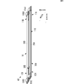
- 1 is an external perspective view of a flat cable including a transmission line according to a first embodiment of the invention. It is a disassembled perspective view which shows the structure of the main transmission line part which concerns on the 1st Embodiment of this invention. It is a disassembled plan view which shows the structure of the main transmission line part which concerns on the 1st Embodiment of this invention. It is sectional drawing which shows the structure of the main transmission line part which concerns on the 1st Embodiment of this invention.
- 1A and 1B are a side cross-sectional view and a plan cross-sectional view illustrating a component configuration of an electronic device according to a first embodiment of the present invention.
- FIG. 1 is an external perspective view of a flat cable including a transmission line according to the first embodiment of the invention.
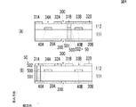
- FIG. 2 is an exploded perspective view showing the structure of the main transmission line section according to the first embodiment of the present invention.
- FIG. 3 is an exploded plan view showing the structure of the main transmission line section according to the first embodiment of the present invention.
- FIG. 4 is a cross-sectional view showing the structure of the main transmission line unit according to the first embodiment of the present invention.
- 4A is a cross-sectional view taken along the line AA shown in FIG. 3
- FIG. 4B is a cross-sectional view taken along the line BB shown in FIG.
- FIG. 1 shows the reference ground conductor side on which the connector is disposed as the upper surface
- the flat cable 60 includes a main transmission line 10, lead transmission lines 11A, 11B, 12A, and 12B, and connectors 61A1, 61A2, 61B1, and 61B2.
- the main transmission line 10 is flat and has a long shape. This long direction is the longitudinal direction of the main transmission line 10 and corresponds to the transmission direction of the high-frequency signal. Further, the direction parallel to the flat plate surface and perpendicular to the longitudinal direction (that is, the transmission direction) is the width direction.
- the main transmission line 10 corresponds to the “transmission line” and the “main line portion” of the present invention.
- the main transmission line 10 includes a dielectric body 110, reference ground conductors 20A and 20B, auxiliary ground conductors 30A and 30B, and signal conductors 40A and 40B.
- the dielectric element body 110 includes a first dielectric layer 111 and a second dielectric layer 112.
- the dielectric body 110 is a flexible flat plate having a predetermined thickness.
- the dielectric body 110 is long and is made of a flexible material such as polyimide or liquid crystal polymer.
- the first dielectric layer 111 and the second dielectric layer 112 may each be a laminate of a plurality of dielectric layers.
- the reference ground conductors 20 ⁇ / b> A and 20 ⁇ / b> B are arranged on one end surface (flat plate surface) of the dielectric body 110, in other words, on the exposed surface of the first dielectric layer 111.
- the reference ground conductors 20 ⁇ / b> A and 20 ⁇ / b> B are long solid conductors and have a shape extending in the same direction as the long direction of the dielectric body 110.
- the reference ground conductors 20A and 20B are arranged with a gap 200 in the width direction.
- the reference ground conductors 20A and 20B are made of a highly conductive material such as copper (Cu).
- the reference ground conductors 20A and 20B are ground conductors that mainly determine the characteristic impedance of the main transmission line 10 and the lead transmission lines 11A, 11B, 12A, and 12B.
- the signal conductors 40A and 40B and the reference ground conductors 20A and 20B are designed so that the characteristic impedance of the main transmission line 10 is 55 ⁇ , which is slightly higher than 50 ⁇ .
- the shapes of the auxiliary ground conductors 30A and 30B are adjusted so that the characteristic impedance of the main transmission line 10 is 50 ⁇ by the signal conductors 40A and 40B, the reference ground conductors 20A and 20B, and auxiliary ground conductors 30A and 30B described later.
- the auxiliary ground conductors 30A and 30B are formed on the other end surface (flat plate surface) of the dielectric body 110, in other words, on the exposed surface of the second dielectric layer 112.
- the auxiliary ground conductors 30 ⁇ / b> A and 30 ⁇ / b> B are elongated and have a shape that extends in the same direction as the longitudinal direction of the dielectric body 110.
- the auxiliary ground conductors 30A and 30B are arranged with a gap 300 in the width direction.
- the auxiliary ground conductor 30 ⁇ / b> A faces the reference ground conductor 20 ⁇ / b> A through the dielectric body 110.
- the auxiliary ground conductor 30B is opposed to the reference ground conductor 20B with the dielectric body 110 interposed therebetween.
- the auxiliary ground conductors 30A and 30B are also made of a highly conductive material such as copper (Cu).
- the auxiliary ground conductor 30A includes long conductors 31A and 32A and a bridge conductor 33A.
- the long conductors 31 ⁇ / b> A and 32 ⁇ / b> A have a long shape extending along the longitudinal direction of the dielectric body 110.
- the long conductors 31 ⁇ / b> A and 32 ⁇ / b> A are formed at a predetermined interval along the width direction of the dielectric body 110.
- the bridge conductor 33 ⁇ / b> A has a shape extending in the width direction of the dielectric body 110.
- a plurality of bridge conductors 33 ⁇ / b> A are formed at intervals along the longitudinal direction of the dielectric body 110.
- an opening 34A is formed between the bridge conductors 33A when viewed from a direction orthogonal to the flat plate surface (as viewed along the thickness direction).
- the auxiliary ground conductor 30A has a ladder shape extending in the longitudinal direction.
- the auxiliary ground conductor 30B includes long conductors 31B and 32B and a bridge conductor 33B.
- the long conductors 31 ⁇ / b> B and 32 ⁇ / b> B have a long shape extending along the longitudinal direction of the dielectric body 110.
- the long conductors 31 ⁇ / b> B and 32 ⁇ / b> B are formed at a predetermined interval along the width direction of the dielectric body 110.
- the bridge conductor 33 ⁇ / b> B has a shape extending in the width direction of the dielectric body 110.
- a plurality of bridge conductors 33 ⁇ / b> B are formed at intervals along the longitudinal direction of the dielectric body 110.
- an opening 34B is formed between the bridge conductors 33B when viewed from a direction orthogonal to the flat plate surface (as viewed along the thickness direction).
- the auxiliary ground conductor 30B has a ladder shape extending in the longitudinal direction.
- the interval in the transmission direction of the bridge conductors 33A and 33B of the auxiliary ground conductors 30A and 30B is designed so that no radiation noise is generated within the use band.
- the auxiliary ground conductors 30A and 30B are ground conductors that also function as shields. Further, as described above, the auxiliary ground conductors 30A and 30B are arranged, for example, for final adjustment so that the characteristic impedance of the main transmission line 10 becomes 50 ⁇ .
- the auxiliary ground conductor 30 ⁇ / b> A is connected to the reference ground conductor 20 ⁇ / b> A via a thickness direction connecting conductor 50 that penetrates the dielectric body 110 in the thickness direction.
- the auxiliary ground conductor 30B is connected to the reference ground conductor 20B through a thickness direction connecting conductor 50 that penetrates the thickness direction.
- the thickness direction connecting conductor 50 is formed at a plurality of locations.
- the thickness direction connecting conductor 50 includes an intermediate conductor pattern 500 and via conductors 501 and 502 as shown in FIG.
- the intermediate conductor pattern 500 is formed on the boundary surface between the first dielectric layer 111 and the second dielectric layer 112.
- the via conductor 501 has a shape penetrating the first dielectric layer 111.
- the via conductor 502 has a shape penetrating the second dielectric layer 112.
- the thickness direction connecting conductor 50 is provided at the intersection of the bridge conductor and the long conductor of each of the auxiliary ground conductors 30A and 30B. Further, the thickness direction connecting conductor 50 has a constant diameter. Accordingly, the auxiliary ground conductors 30A and 30B in the portion where the thickness direction connecting conductor 50 is provided project in the width direction (opening direction) correspondingly. Further, the signal conductors 40A and 40B have notches that become narrow in the width direction in correspondence with the protrusions of the thickness direction connecting conductor 50 and the auxiliary ground conductors 30A and 30B. The characteristic impedance of the main transmission line 10 is designed in consideration of this point.
- the thickness direction connecting conductors 50 are provided alternately one by one in the width direction at the intersections between the bridge conductors and the long conductors of the auxiliary ground conductors 30A and 30B. If two thickness direction connecting conductors 50 are provided in a certain width direction, the signal conductors 40A and 40B must be designed to be narrow in the width direction in a portion overlapping the bridge conductor. As a result, the transmission characteristics of the signal conductors 40A and 40B may be deteriorated. In order to avoid this, the main transmission line 10 must be widened. In the present embodiment, since only one thickness direction connecting conductor 50 is provided in a certain width direction, the width of the signal conductors 40A and 40B can be suppressed, and the width of the main transmission line 10 can be increased. There is no need to do.
- the thickness direction connecting conductors 50 are provided alternately one by one in the width direction at the intersections of the bridge conductors and the long conductors of the auxiliary ground conductors 30A and 30B, isolation between adjacent individual transmission units is provided. In addition, it is possible to secure isolation from external circuits. Further, the ground potentials of the auxiliary ground conductors 30A and 30B can be well balanced.
- the signal conductors 40A and 40B have a flat film shape and are formed between the first dielectric layer 111 and the second dielectric layer 112.
- the signal conductors 40 ⁇ / b> A and 40 ⁇ / b> B are arranged at a predetermined interval along the width direction of the dielectric body 110.
- the signal conductors 40A and 40B are also made of a highly conductive material such as copper (Cu).
- the signal conductor 40A is disposed so as to face the reference ground conductor 20A via the first dielectric layer 111 and to face the auxiliary ground conductor 30A via the second dielectric layer 112.
- the signal conductor 40A is located approximately at the center in the width direction of the reference ground conductor 20A, and is disposed at approximately the center in the width direction of the opening 34A of the auxiliary ground conductor 30A.
- the signal conductor 40B is disposed so as to face the reference ground conductor 20B via the first dielectric layer 111 and face the auxiliary ground conductor 30B via the second dielectric layer 112.
- the signal conductor 40B is positioned approximately at the center in the width direction of the reference ground conductor 20B, and is disposed at approximately the center in the width direction of the opening 34B of the auxiliary ground conductor 30B.
- the main transmission line 10 has a structure in which the first main line and the second main line are arranged with an interval in the width direction based on the single dielectric body 110.
- the first main line includes a reference ground conductor 20A, an auxiliary ground conductor 30A, a signal conductor 40A, and a dielectric element body 110.
- the second main line includes a reference ground conductor 20B, an auxiliary ground conductor 30B, a signal conductor 40B, and a dielectric body 110.
- the arrangement positions along the longitudinal direction of the bridge conductor 33A of the first main line and the bridge conductor 33B of the second main line are different. More specifically, the bridge conductor 33A of the first main line is disposed at an intermediate position between adjacent bridge conductors 33B in the second main line.
- the intermediate position between the adjacent bridge conductors is a portion where the distance from the bridge conductor is farthest, and the electric field strength and magnetic field strength due to the high-frequency signal are the largest.
- the maximum point of the electric field strength and the maximum point of the magnetic field strength by the high-frequency signal transmitted through the first main line, and the maximum point and the magnetic field strength of the electric field strength by the high-frequency signal transmitted through the second main line. are not aligned along the longitudinal direction. Thereby, the isolation of a 1st main line and a 2nd main line can be ensured highly, and the crosstalk of the high frequency signal which transmits a 1st main line, and the high frequency signal which transmits a 2nd main line can be suppressed. This is because the electric field distribution and magnetic field distribution of the high-frequency signal transmitted through the first and second main lines depend on the position and pattern of the bridge conductors 33A and 33B.
- the single dielectric element 110 is used in the present embodiment, it can be formed smaller than the case where the dielectric element 110 is used for each high-frequency signal. Further, by using the flat dielectric element 110, the transmission line can be made thinner than the coaxial cable.
- the reference ground conductors 20A and 20B by arranging the reference ground conductors 20A and 20B with the gap 200 in the width direction, it is possible to suppress the first main line and the second main line from being coupled via the ground. . Thereby, the isolation between a 1st main line and a 2nd main line can be ensured still higher.
- the positional relationship between the bridge conductors 33A and 33B is preferably set to an intermediate position along the longitudinal direction as in the present embodiment from the viewpoint of isolation, but the position along the longitudinal direction may be different. That's fine.
- the thickness direction connecting conductor 50 is preferably formed at least at a position where the long conductors 32A and 31B on the side where the first main line and the second main line are close to each other and the reference ground conductors 20A and 20B face each other. .
- the first main line and the second main line are separated by the thickness direction connecting conductor 50 connected to the ground potential, so that the first main line in the dielectric layer 111 and Electromagnetic field coupling with the second main line can be suppressed.
- the lead transmission lines 11 ⁇ / b> A and 11 ⁇ / b> B are connected to one end in the longitudinal direction of the main transmission line 10.
- the lead transmission lines 11A and 11B are arranged at a predetermined interval in the width direction.
- the lead transmission lines 12 ⁇ / b> A and 12 ⁇ / b> B are connected to the other end in the longitudinal direction of the main transmission line 10.
- the lead transmission lines 12A and 12B are arranged at a predetermined interval in the width direction.
- the lead-out transmission lines 11A and 12A are arranged at both ends in the longitudinal direction with the main transmission line 10 interposed therebetween.
- the lead transmission lines 11B and 12B are disposed at both ends in the longitudinal direction with the main transmission line 10 interposed therebetween.
- the lead transmission lines 11 A and 11 B are connected to the first main line of the main transmission line 10, and the lead transmission lines 12 A and 12 B are connected to the second main line of the main transmission line 10.
- the lead transmission lines 11A, 11B, 12A, 12B have the following structure.
- the lead transmission lines 11A, 11B, 12A, and 12B are composed of a dielectric element body in which a signal conductor is arranged at a predetermined position in the thickness direction using a reference ground conductor and an auxiliary ground conductor. It consists of a sandwiched structure.
- the signal conductors of the lead transmission lines 11A and 12A are connected to the signal conductor 40A of the main transmission line 10.
- the reference ground conductors of the lead transmission lines 11A and 12A are connected to the reference ground conductor 20A of the main transmission line 10.
- the auxiliary ground conductors of the lead transmission lines 11A and 12A are connected to the auxiliary ground conductor 30A of the main transmission line 10. The functions of the reference ground conductor and the auxiliary ground conductor are the same as described above.
- the signal conductors of the lead transmission lines 11B and 12B are connected to the signal conductor 40B of the main transmission line 10.
- the reference ground conductors of the lead transmission lines 11B and 12B are connected to the reference ground conductor 20B of the main transmission line 10.
- the auxiliary ground conductors of the lead transmission lines 11B and 12B are connected to the auxiliary ground conductor 30B of the main transmission line 10.
- the widths of the first main line and the second main line and the widths of the lead transmission lines 11A, 11B, 12A, and 12B are different, the widths of the first main line and the second main line and the lead transmission lines 11A, 11B, and 12A are different.
- 12B may be structured such that the distance between the long conductors of the auxiliary ground conductor (length in the width direction) gradually changes. Thereby, the transmission loss between the widths of the first main line and the second main line and the lead transmission lines 11A, 11B, 12A, 12B can be suppressed.
- the connector 61A1 is disposed at the end of the lead transmission line 11A (the end opposite to the main transmission line 10).
- the connector 61A2 is disposed at the end of the lead transmission line 12A (the end opposite to the main transmission line 10).
- the connector 61B1 is disposed at the end of the lead transmission line 11B (the end opposite to the main transmission line 10).
- the connector 61B2 is disposed at the end of the lead transmission line 12B (the end opposite to the main transmission line 10).
- the connectors 61A1 and 61B1 are arranged on one end side of the main transmission line 10, and 61A2 and 61B2 are arranged on the other end face side of the main transmission line 10.
- the connector 61A1 is electrically connected to the lead transmission line 11A
- the connector 61A2 is electrically connected to the lead transmission line 12A
- the connector 61B1 is electrically connected to the lead transmission line 11B
- the connector 61B2 is electrically connected to the lead transmission line 12B.
- coaxial type connectors can be used as the connectors 61A1, 61A2, 61B1, and 61B2 for example.
- a protective film (not shown) may be formed on both flat surfaces of the flat cable 60.
- a flat cable capable of transmitting these high-frequency signals with high isolation between a plurality of high-frequency signals can be formed small and thin.
- the flat cable 60 having such a structure is manufactured as follows, for example.
- the lead-out transmission lines 11A, 11B, 12A, and 12B are also formed integrally with the main transmission line 10.
- first, second, and third insulating films with a single-sided copper paste with a copper foil stretched over the entire surface of one side are prepared.
- a liquid crystal polymer is used as the insulating film.
- the reference ground conductors 20A and 20B are formed on one end face of the first insulating film by patterning.
- Signal conductors 40A and 40B are formed on the other end surface of the second insulating film by patterning.
- Auxiliary ground conductors 30A and 30B are formed by patterning on the other end surface side of the third insulating film. Then, the reference ground conductor 20A and the auxiliary ground conductor 30A are connected, and the first, second, and third insulating films are connected in the thickness direction so as to connect the reference ground conductor 20B and the auxiliary ground conductor 30B.
- a conductor 50 is formed.
- a through hole is formed by irradiating a laser beam from the side of the first, second, and third insulating films where the copper foil is not stretched, and the through hole is filled with a conductive paste.
- the thickness direction connecting conductor 50 can be formed.
- the reference ground conductor 20A and the auxiliary ground conductor 30A are opposed to each other with the signal conductor 40A interposed therebetween, and the reference ground conductor 20B and the auxiliary ground conductor 30B are opposed to each other with the signal conductor 40B interposed therebetween.
- a dielectric body 110 is formed by bonding a third insulating film.
- the connectors 61A1, 61A2, 61B1, 61B2 are installed on the lead transmission lines 11A, 11B, 12A, 12B arranged at both ends in the longitudinal direction of the flat cable 60.
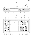
- FIG. 5A is a side cross-sectional view illustrating a component configuration of the portable electronic device according to the first embodiment of the present invention
- FIG. 5B is a plan cross-sectional view illustrating the component configuration of the portable electronic device. is there.
- the portable electronic device 1 includes a thin device casing 2.
- the device casing 2 mounted circuit boards 3A and 3B, which are circuit elements, and a battery pack 4 are arranged.
- a plurality of IC chips 5 and mounting components 6 are mounted on the surfaces of the mounting circuit boards 3A and 3B.
- the mounting circuit boards 3A and 3B and the battery pack 4 are installed in the equipment casing 2 so that the battery pack 4 is disposed between the mounting circuit boards 3A and 3B when the equipment casing 2 is viewed in plan.
- the device housing 2 is formed as thin as possible, the distance between the battery pack 4 and the device housing 2 is extremely narrow in the thickness direction of the device housing 2. Therefore, a coaxial cable cannot be arranged between them.
- the flat cable 60 shown in the present embodiment is arranged so that the thickness direction of the flat cable 60 and the thickness direction of the device housing 2 coincide with each other. A flat cable 60 can be passed between them. As a result, the mounted circuit boards 3A and 3B which are spaced apart from each other with the battery pack 4 disposed in the middle can be connected by the flat cable 60.
- connection position of the flat cable 60 to the mounting circuit boards 3A and 3B and the installation surface of the flat cable 60 of the battery pack 4 are different in the thickness direction of the device housing 2, and the flat cable 60 must be bent and connected. Even when it is necessary, by using the structure of this embodiment, it is possible to transmit a high-frequency signal while suppressing transmission loss.
- the area for transmitting the plurality of high-frequency signals can be reduced, and space can be saved. At this time, the transmission loss of each high-frequency signal can be reduced and transmitted.
- FIG. 6 is an exploded plan view showing the structure of the main transmission line according to the second embodiment of the present invention.
- the main transmission line 10 'of the present embodiment is different from the main transmission line 10 according to the first embodiment in the structure of the reference ground conductor and the auxiliary ground conductor, and the other configurations are the same. Therefore, only different points from the main transmission line 10 according to the first embodiment will be specifically described.
- the reference ground conductors 20A and 20B are connected by a connecting conductor portion 201.
- the connecting conductor portion 201 corresponds to the “first connecting conductor portion” of the present invention.
- the connecting conductor portion 201 is partially formed at a predetermined position along the longitudinal direction of the reference ground conductors 20A and 20B (the transmission direction of the high-frequency signal to be transmitted). In other words, the connecting conductor portion 201 is formed so as to partially fill the gap 200. It is sufficient that at least one connecting conductor portion 201 is formed.
- the gap 200 is secured while ensuring flexibility by the gap 200 not filled with the connecting conductor portion 201.
- the resonance frequency of the unnecessary high-frequency signal generated by providing can be shifted to the high frequency side. Thereby, transmission loss can be reduced.
- the auxiliary ground conductors 30 ⁇ / b> A and 30 ⁇ / b> B are connected by a connecting conductor portion 301.
- the connecting conductor portion 301 corresponds to the “second connecting conductor portion” of the present invention.
- the connecting conductor portion 301 is partially formed at a predetermined position along the longitudinal direction of the auxiliary ground conductors 30A and 30B. In other words, the connecting conductor portion 301 is formed so as to partially fill the gap 300. It is sufficient that at least one connecting conductor portion 301 is formed.
- the gap 300 is formed while ensuring flexibility by the gap 300 not filled with the connecting conductor portion 301.
- the resonance frequency of the unnecessary high-frequency signal generated by providing can be shifted to the high frequency side. Thereby, transmission loss can be reduced.
- the main transmission line 10 is viewed in plan so that the connection conductor portion 201 and the connection conductor portion 301 overlap with each other, and the connection conductor portions 201 and 301 along the longitudinal direction of the main transmission line 10. It is preferable to form the thickness direction connecting conductor 53 at a position where is formed.
- the thickness direction connecting conductor 53 connects the connecting conductor portions 201 and 301.
- the thickness direction connecting conductor 53 connects the reference ground conductor 20A at and near the position to which the connecting conductor portion 201 is connected and the auxiliary ground conductor 30A at and near the position to which the connecting conductor portion 301 is connected, or the connecting conductor portion 201. Is connected to the reference ground conductor 20B at and near the position where the connecting conductor portion 301 is connected and the auxiliary ground conductor 30B at and near the position where the connecting conductor portion 301 is connected.
- a plurality of the thickness direction connecting conductors 53 are provided at different positions along the longitudinal direction.
- the thickness direction connection conductor 53 it is possible to ensure isolation between the first main line and the second main line.
- opening 211 is so-called conductor non-forming portions in the connecting conductor portions 201 and 301.
- These openings 211 are so-called conductor non-forming portions in the connecting conductor portions 201 and 301.
- a decrease in flexibility due to the connecting conductor portions 201 and 301 can be mitigated.
- the magnetic coupling between the first main line and the second main line via the openings 34A and 34B provided in the auxiliary ground conductors 30A and 30B. can be weakened.
- the thickness direction connecting conductor 53 in a region sandwiched between the openings 211 and 311 and the signal conductors 40A and 40B.
- At least one of the connecting conductor portions 201 and 301 may be formed.
- FIG. 7 is an exploded plan view showing the structure of the main transmission line according to the third embodiment of the present invention.
- the main transmission line 10A of the present embodiment is different from the main transmission line 10 according to the first embodiment in the structure of the reference ground conductor, and the other configurations are the same. Therefore, only different points from the main transmission line 10 according to the first embodiment will be specifically described.
- the main transmission line 10 ⁇ / b> A includes a reference ground conductor 20.
- the reference ground conductor 20 is obtained by integrating the reference ground conductors 20A and 20B shown in the first embodiment. Even if it is such a structure, the effect similar to 1st Embodiment can be acquired. Furthermore, in the configuration of the present embodiment, it is not necessary to provide the gap 200, so that the formation of the reference ground conductor is facilitated.
- FIG. 8 is an exploded plan view showing the structure of the main transmission line section according to the fourth embodiment of the present invention.
- the main transmission line 10B of the present embodiment is different from the main transmission line 10A according to the third embodiment in the structure of the auxiliary ground conductor, and the other configurations are the same. Therefore, only different points from the main transmission line 10A according to the third embodiment will be specifically described.
- the auxiliary ground conductors 30A1 and 30A2 have a common long conductor 312 in the width direction opposite to each other shared by the first main line and the second main line.
- variety of the main transmission line 10 can be made narrower than the structure which does not use a common elongate conductor by the 1st main line and the 2nd main line.
- the thickness direction connecting conductor 50 provided on the long conductor of the portion shared by the first main line and the second main line has the bridge conductors 33A and 33B along the longitudinal direction. It is formed in the middle position of the arrangement position.
- the ground is installed at a position where the opening 34A of the first main line and the opening 34B of the second main line are adjacent to each other in the width direction. Accordingly, the isolation between the first main line and the second main line can be further increased, and crosstalk between the high-frequency signal transmitted through the first main line and the high-frequency signal transmitted through the second main line is further suppressed. it can.
- This arrangement structure of the thickness direction connection conductors 50 may be applied even when the long conductors on the side where the first main line and the second main line face each other are not shared, but the width of the long conductors is connected in the thickness direction. Since it is necessary to make it larger than the diameter of the conductor 50, the width of the main transmission line 10 will become wide. However, in the configuration of the present embodiment, the long conductor on the side where the first main line and the second main line face each other is shared. Therefore, even if the width of the long conductor is increased, the width of the main transmission line 10 can be reduced as much as possible, and this configuration works more effectively.
- FIG. 9 is an exploded plan view showing the structure of the main transmission line section according to the fifth embodiment of the present invention.
- the main transmission line 10C of the present embodiment is different from the main transmission line 10B according to the fourth embodiment in the structure of the auxiliary ground conductor, and the other configurations are the same. Therefore, only different points from the main transmission line 10B according to the fourth embodiment will be specifically described.
- the thickness direction connection conductor 50 is not provided at a position overlapping the long conductors 31An and 32Bn at both ends of the dielectric body 110 in the width direction.
- the width of the long conductors 31An and 32Bn can be reduced.
- the width of the signal conductors 40A and 40B can be increased and transmission loss can be reduced. Further, when the width of the dielectric body 110 is changed, the width of the dielectric body 110 can be reduced.
- the thickness direction connecting conductors 50 are disposed at both ends of the dielectric element body 110 in the width direction. By arranging such a thickness direction connection conductor 50, external interference between the first main line and the second main line can be suppressed.
- the width of the opening in the main transmission line is made constant has been shown.
- the width of the opening may be gradually increased from the end connected to the bridge conductor toward the center in the longitudinal direction of the opening.
- the example in which the width of the signal conductor of the main transmission line is made constant is shown.
- the width of the signal conductor in the portion facing the opening may be increased.
- the signal conductor is widened so as not to overlap the long conductor when the flat cable is viewed in the thickness direction. Thereby, the high frequency resistance of a signal conductor can be reduced and the conductor loss of a flat cable can be reduced.
- FIG. 10 is an external perspective view of a flat cable including a transmission line according to the sixth embodiment of the present invention.
- FIG. 11 is an exploded plan view showing the structure of a flat cable lead-out transmission line according to the sixth embodiment of the present invention.
- the structure of the outgoing transmission line of the one end of the flat cable in the elongate direction is illustrated, but the outgoing transmission line of the other end also has the same structure.
- the flat cable 60D shown in this embodiment has connectors 61A1, 61A2, 61B1, and 61B2 arranged on the auxiliary ground conductor side, and the reference ground conductor is a signal conductor. It is arrange
- the flat cable 60D includes a main transmission line 10D, lead transmission lines 11AD, 11BD, 12AD, 12BD, and connectors 61A1, 61A2, 61B1, 61B2.
- the main transmission line 10D has an auxiliary ground disposed on the connector side of the signal conductor and a reference ground disposed on the opposite side of the signal conductor connector. Consists of structure.
- the lead transmission lines 11BD and 12BD have a long shape extending in the same direction as the long direction of the main transmission line 10D, similarly to the lead transmission lines 11B and 12B shown in the first embodiment. These lead transmission lines 11BD and 12BD correspond to the “first lead transmission line” of the present invention.
- the lead-out transmission lines 11AD and 12AD have a linear part ReS extending in the same direction as the longitudinal direction of the main transmission line 10D and a curved part ReC that curves in a direction different from the longitudinal direction. These lead transmission lines 11AD and 12AD correspond to the “second lead transmission line” of the present invention.
- the lead-out transmission line 11BD includes a long dielectric element body 110BN extending along the long direction of the main transmission line 10D.
- One end of the dielectric body 110BN in the longitudinal direction is connected to the dielectric body 110 constituting the main line conductor.
- the other end of the dielectric body 110BN is partially widened. That is, the length of the other end of the dielectric element body 110BN in the short side direction is longer than that of the dielectric element body 110 side.
- an auxiliary ground conductor 30BN, a signal conductor 40BN, and a reference ground conductor 20BN are arranged at intervals along the thickness direction.
- the auxiliary ground conductor 30BN includes long conductors 31BN and 32BN extending along the long direction of the dielectric body 110BN.
- the long conductor 31BN is connected to the long conductor 31B of the main transmission line 10D, and the long conductor 32BN is connected to the long conductor 32B of the main transmission line 10D.
- the long conductors 31BN and 32BN are formed near both ends in the short direction of the dielectric element body 110BN.
- the long conductors 31BN and 32BN are connected by a plurality of bridge conductors 33BN disposed at intervals along the extending direction.
- the long conductors 31BN and 32BN are connected by a connector connecting conductor 43BN at the other end of the dielectric element body 110BN (the end opposite to the side connected to the dielectric element body 110).
- the connector connecting conductor 43BN is formed over substantially the entire wide portion at the other end of the dielectric element body 110BN, and an opening in which no conductor is formed is provided at the center.
- a connector connecting conductor 42BN is formed in the center of the opening so as not to be connected to the connector connecting conductor 43BN.
- the signal conductor 40BN has a shape extending along the longitudinal direction of the dielectric element body 110BN, and is disposed at the center position in the short direction of the dielectric element body 110BN.
- the signal conductor 40BN is connected to the signal conductor 40B of the main transmission line 10D.
- the signal conductor 40BN is arranged so as not to overlap the long conductors 31BN and 32BN of the auxiliary ground conductor 30BN in plan view of the dielectric body 110BN.
- the signal conductor 40BN is connected to the connector connecting conductor 41BN at the other end of the dielectric body 110BN.
- the connector connecting conductor 41BN is connected to the connector connecting auxiliary conductor 42BN through the thickness direction connecting conductor 50.
- the reference ground conductor 20BN has a shape extending along the longitudinal direction of the dielectric body 110BN.
- the width (length in the short direction) of the reference ground conductor 20BN is substantially the same as the width (length in the short direction) of the dielectric element body 110BN.
- the reference ground conductor 20BN is connected to the long conductors 31BN and 32BN of the auxiliary ground conductor 30BN through the thickness direction connecting conductor 50.
- the reference ground conductor 20BN is connected to the connector connecting conductor 44BN at the other end of the dielectric body 110BN.
- the connector connecting conductor 44BN is connected to the connector connecting auxiliary conductor 41BN via the thickness direction connecting conductor 50.
- the lead-out transmission line 11AD has an elongated shape having a linear part ReS extending in the same direction as the longitudinal direction of the main transmission line 10D and a curved part ReC curved in a direction different from the longitudinal direction.
- a dielectric body 110AN is provided. One end in the longitudinal direction of the dielectric body 110AN is connected to the dielectric body 110 constituting the main line conductor. The other end of the dielectric body 110AN is partially wide. That is, the length of the other end of the dielectric body 110AN in the short direction is longer than that of the dielectric body 110 side.
- an auxiliary ground conductor 30AN, a signal conductor 40AN, and a reference ground conductor 20AN are arranged at intervals along the thickness direction.
- the auxiliary ground conductor 30AN includes long conductors 31AN and 32AN.
- the long conductors 31AN and 32AN have a shape extending along the long direction of the dielectric body 110AN in the straight portion ReS, and from a shape extending along the curved shape of the dielectric body 110AN in the curved portion ReC. Become.
- the long conductor 31AN is connected to the long conductor 31A of the main transmission line 10D
- the long conductor 32AN is connected to the long conductor 32A of the main transmission line 10D.
- the long conductors 31AN and 3ABN are formed near both ends of the dielectric body 110AN in the short direction.
- the long conductors 31AN and 32AN are connected by a plurality of bridge conductors 33AN arranged at intervals along the extending direction.
- the long conductors 31AN and 32AN are connected by a connector connecting conductor 43AN at the other end of the dielectric body 110AN (the end opposite to the side connected to the dielectric body 110).
- the connector connecting conductor 43AN is formed over substantially the entire wide portion of the other end of the dielectric body 110AN, and an opening in which no conductor is formed is provided at the center.
- a connector connecting conductor 42AN is formed in the center of the opening so as not to be connected to the connector connecting conductor 43AN.
- the signal conductor 40AN has a shape that extends along the longitudinal direction of the dielectric body 110AN in the straight portion ReS, and a shape that extends along the curved shape of the dielectric body 110AN in the curved portion ReC.
- the signal conductor 40AN is arranged at the center position in the short direction of the dielectric body 110AN.
- the signal conductor 40AN is connected to the signal conductor 40A of the main transmission line 10D.
- the signal conductor 40AN is disposed so as not to overlap with the long conductors 31AN and 32AN of the auxiliary ground conductor 30AN in a plan view of the dielectric body 110AN.
- the signal conductor 40AN is connected to the connector connecting conductor 41AN at the other end of the dielectric body 110AN.
- the connector connecting conductor 41AN is connected to the connector connecting auxiliary conductor 42AN through the thickness direction connecting conductor 50.
- the reference ground conductor 20AN has a shape extending along the longitudinal direction of the dielectric body 110AN in the straight portion ReS, and has a shape extending along the curved shape of the dielectric body 110AN in the curved portion ReC.
- the width (length in the short direction) of the reference ground conductor 20AN is substantially the same as the width (length in the short direction) of the dielectric body 110AN.
- the reference ground conductor 20AN is connected to the long conductors 31AN and 32AN of the auxiliary ground conductor 30AN through the thickness direction connecting conductor 50 only at the straight line portion ReS.
- the reference ground conductor 20AN is connected to the connector connecting conductor 44AN at the other end of the dielectric body 110AN.
- the connector connecting conductor 44AN is connected to the connector connecting auxiliary conductor 41AN via the thickness direction connecting conductor 50.
- the connectors 61B1 and 61B2 of the linear lead transmission lines 11BD and 12BD are first connected (fixed) to the mounting circuit board, and the flat cable 60D is mounted. Secure to the circuit board. Thereby, the flat cable 60D can be temporarily fixed to the mounting circuit board.
- the connectors 61A1 and 61A2 of the lead transmission lines 11AD and 12AD having the curved portion ReC are connected (fixed) to the mounting circuit board.
- the lead transmission lines 11AD and 12AD can be provided with a degree of freedom for handling. Thereby, even if there are many connector connection locations, the connector can be easily connected (fixed) to the mounting circuit board.
- the bending direction ReC since the bending direction ReC is not provided with the thickness direction connection conductor 50, the bending portion ReC has higher flexibility than the straight portion ReS. Therefore, the connector can be more easily connected (fixed) to the mounting circuit board. In addition, a change in characteristic impedance due to expansion / contraction of the bending portion ReC can be suppressed.
- one of the two lead transmission lines connected to one end in the longitudinal direction of the main transmission line 10D has a linear structure with relatively low flexibility, and the other relatively Although a structure having a highly flexible curved portion is provided, when three or more lead transmission lines are provided, at least one linear structure and a structure having a curved portion may be provided.
- the linear distance from the main transmission line 10D to the connector is the same in the transmission lines 11AD and 11BD and the same in the transmission lines 12AD and 12BD in the state where no external force is applied. Indicated. However, this linear distance may be different.
Landscapes
- Engineering & Computer Science (AREA)
- Microelectronics & Electronic Packaging (AREA)
- Physics & Mathematics (AREA)
- Electromagnetism (AREA)
- Waveguides (AREA)
- Structure Of Printed Boards (AREA)
- Insulated Conductors (AREA)
Abstract
La présente invention concerne une ligne de transmission principale (10) équipée d'un long élément diélectrique (110). Selon l'invention, de longs conducteurs de signaux (40A, 40B) sont disposés à l'intérieur de l'élément diélectrique (110) de sorte que des intervalles les séparent dans la direction de la largeur. Un conducteur de masse de référence (20A) et un conducteur de masse auxiliaire (30A) sont disposés de façon à prendre en sandwich le conducteur de signaux (40A) dans la direction de son épaisseur. Un conducteur de masse de référence (20B) et un conducteur de masse auxiliaire (30B) sont disposés de façon à prendre en sandwich le conducteur de signaux (40B) dans la direction de son épaisseur. Le conducteur de masse auxiliaire (30A) est équipé de longs conducteurs (31A, 32A) et d'un conducteur en pont (33A), tandis que le conducteur de masse auxiliaire (30B) est équipé de longs conducteurs (31B, 32B) et d'un connecteur en pont (33B). Les conducteurs en pont (33A, 33B) sont situés à des positions différentes dans la direction de la longueur.
Priority Applications (3)
| Application Number | Priority Date | Filing Date | Title |
|---|---|---|---|
| JP2014529737A JP5696819B2 (ja) | 2013-01-23 | 2014-01-15 | 伝送線路、および電子機器 |
| CN201480003002.4A CN104798248B (zh) | 2013-01-23 | 2014-01-15 | 传输线路及电子设备 |
| US14/796,027 US9666925B2 (en) | 2013-01-23 | 2015-07-10 | Transmission line, a transmission line apparatus, and an electronic device |
Applications Claiming Priority (6)
| Application Number | Priority Date | Filing Date | Title |
|---|---|---|---|
| JP2013-010009 | 2013-01-23 | ||
| JP2013010009 | 2013-01-23 | ||
| JP2013145039 | 2013-07-10 | ||
| JP2013-145039 | 2013-07-10 | ||
| JP2013-232710 | 2013-11-11 | ||
| JP2013232710 | 2013-11-11 |
Related Child Applications (1)
| Application Number | Title | Priority Date | Filing Date |
|---|---|---|---|
| US14/796,027 Continuation US9666925B2 (en) | 2013-01-23 | 2015-07-10 | Transmission line, a transmission line apparatus, and an electronic device |
Publications (1)
| Publication Number | Publication Date |
|---|---|
| WO2014115607A1 true WO2014115607A1 (fr) | 2014-07-31 |
Family
ID=51227399
Family Applications (1)
| Application Number | Title | Priority Date | Filing Date |
|---|---|---|---|
| PCT/JP2014/050493 Ceased WO2014115607A1 (fr) | 2013-01-23 | 2014-01-15 | Ligne de transmission et dispositif électronique |
Country Status (4)
| Country | Link |
|---|---|
| US (1) | US9666925B2 (fr) |
| JP (1) | JP5696819B2 (fr) |
| CN (1) | CN104798248B (fr) |
| WO (1) | WO2014115607A1 (fr) |
Cited By (4)
| Publication number | Priority date | Publication date | Assignee | Title |
|---|---|---|---|---|
| WO2018139382A1 (fr) * | 2017-01-27 | 2018-08-02 | 株式会社村田製作所 | Substrat multicouche et dispositif électronique |
| JP2019516231A (ja) * | 2016-02-26 | 2019-06-13 | ギガレーン カンパニー リミテッドGigalane Co., Ltd. | フレキシブルプリント回路基板 |
| US10749236B2 (en) | 2017-01-19 | 2020-08-18 | Murata Manufacturing Co., Ltd. | Transmission line |
| JPWO2019235558A1 (ja) * | 2018-06-07 | 2021-06-10 | 株式会社村田製作所 | 多層基板、電子機器および多層基板の製造方法 |
Families Citing this family (4)
| Publication number | Priority date | Publication date | Assignee | Title |
|---|---|---|---|---|
| CN105428770B (zh) * | 2015-11-30 | 2018-10-23 | 上海宇航系统工程研究所 | 一种平衡式双线传输线 |
| KR102580988B1 (ko) * | 2016-05-02 | 2023-09-21 | 엘지이노텍 주식회사 | 인쇄회로기판 및 이를 포함하는 전자부품패키지 |
| JP6841287B2 (ja) | 2017-02-16 | 2021-03-10 | 株式会社村田製作所 | 多層基板 |
| CN116209136B (zh) | 2021-11-30 | 2023-12-01 | 荣耀终端有限公司 | 一种信号传输结构、电子设备及pcb板 |
Citations (3)
| Publication number | Priority date | Publication date | Assignee | Title |
|---|---|---|---|---|
| WO2010150588A1 (fr) * | 2009-06-24 | 2010-12-29 | 株式会社村田製作所 | Ligne de transmission de signal |
| WO2011007660A1 (fr) * | 2009-07-13 | 2011-01-20 | 株式会社村田製作所 | Ligne de signal et carte de circuit imprimé |
| WO2013190859A1 (fr) * | 2012-06-19 | 2013-12-27 | 株式会社村田製作所 | Câble multi-cœur stratifié |
Family Cites Families (5)
| Publication number | Priority date | Publication date | Assignee | Title |
|---|---|---|---|---|
| JP2002335107A (ja) * | 2001-05-08 | 2002-11-22 | Nec Corp | 伝送線路型コンポーネント |
| KR100400081B1 (ko) * | 2001-11-24 | 2003-09-29 | 한국전자통신연구원 | 광전 모듈용 서브마운트 및 이를 이용한 실장 방법 |
| JP4731788B2 (ja) * | 2002-10-02 | 2011-07-27 | キヤノン株式会社 | ケーブル配線構造およびケーブル配線構造を有する電子機器 |
| JP5041108B2 (ja) * | 2010-12-03 | 2012-10-03 | 株式会社村田製作所 | 高周波信号線路 |
| KR101454720B1 (ko) * | 2010-12-03 | 2014-10-27 | 가부시키가이샤 무라타 세이사쿠쇼 | 고주파 신호선로 및 전자기기 |
-
2014
- 2014-01-15 WO PCT/JP2014/050493 patent/WO2014115607A1/fr not_active Ceased
- 2014-01-15 JP JP2014529737A patent/JP5696819B2/ja active Active
- 2014-01-15 CN CN201480003002.4A patent/CN104798248B/zh active Active
-
2015
- 2015-07-10 US US14/796,027 patent/US9666925B2/en active Active
Patent Citations (3)
| Publication number | Priority date | Publication date | Assignee | Title |
|---|---|---|---|---|
| WO2010150588A1 (fr) * | 2009-06-24 | 2010-12-29 | 株式会社村田製作所 | Ligne de transmission de signal |
| WO2011007660A1 (fr) * | 2009-07-13 | 2011-01-20 | 株式会社村田製作所 | Ligne de signal et carte de circuit imprimé |
| WO2013190859A1 (fr) * | 2012-06-19 | 2013-12-27 | 株式会社村田製作所 | Câble multi-cœur stratifié |
Cited By (13)
| Publication number | Priority date | Publication date | Assignee | Title |
|---|---|---|---|---|
| JP2021073701A (ja) * | 2016-02-26 | 2021-05-13 | ギガレーン カンパニー リミテッドGigalane Co., Ltd. | フレキシブルプリント回路基板 |
| JP2019516231A (ja) * | 2016-02-26 | 2019-06-13 | ギガレーン カンパニー リミテッドGigalane Co., Ltd. | フレキシブルプリント回路基板 |
| JP7048774B2 (ja) | 2016-02-26 | 2022-04-05 | ギガレーン カンパニー リミテッド | フレキシブルプリント回路基板 |
| US10624209B2 (en) | 2016-02-26 | 2020-04-14 | Gigalane Co., Ltd. | Flexible printed circuit board |
| US10749236B2 (en) | 2017-01-19 | 2020-08-18 | Murata Manufacturing Co., Ltd. | Transmission line |
| US10873120B2 (en) | 2017-01-27 | 2020-12-22 | Murata Manufacturing Co., Ltd. | Multilayer board and electronic device |
| WO2018139382A1 (fr) * | 2017-01-27 | 2018-08-02 | 株式会社村田製作所 | Substrat multicouche et dispositif électronique |
| JP2020167427A (ja) * | 2017-01-27 | 2020-10-08 | 株式会社村田製作所 | 多層基板および電子機器 |
| JPWO2018139382A1 (ja) * | 2017-01-27 | 2019-06-27 | 株式会社村田製作所 | 多層基板および電子機器 |
| JP7408493B2 (ja) | 2017-01-27 | 2024-01-05 | 株式会社村田製作所 | 多層基板および電子機器 |
| JPWO2019235558A1 (ja) * | 2018-06-07 | 2021-06-10 | 株式会社村田製作所 | 多層基板、電子機器および多層基板の製造方法 |
| JP7001158B2 (ja) | 2018-06-07 | 2022-01-19 | 株式会社村田製作所 | 多層基板、電子機器および多層基板の製造方法 |
| US11291125B2 (en) | 2018-06-07 | 2022-03-29 | Murata Manufacturing Co., Ltd. | Multilayer substrate, electronic device, and method of manufacturing multilayer substrate |
Also Published As
| Publication number | Publication date |
|---|---|
| CN104798248B (zh) | 2017-03-15 |
| US20150318595A1 (en) | 2015-11-05 |
| CN104798248A (zh) | 2015-07-22 |
| US9666925B2 (en) | 2017-05-30 |
| JPWO2014115607A1 (ja) | 2017-01-26 |
| JP5696819B2 (ja) | 2015-04-08 |
Similar Documents
| Publication | Publication Date | Title |
|---|---|---|
| JP5696819B2 (ja) | 伝送線路、および電子機器 | |
| US11581622B2 (en) | Transmission line and electronic device | |
| JP5842850B2 (ja) | フラットケーブルおよび電子機器 | |
| JP5743037B2 (ja) | 樹脂多層基板および電子機器 | |
| JP5967290B2 (ja) | 高周波伝送線路 | |
| CN205584615U (zh) | 信号传输元器件及电子设备 | |
| JP6137360B2 (ja) | 高周波線路及び電子機器 | |
| JP5527493B1 (ja) | フラットケーブルおよび電子機器 | |
| JP5527494B1 (ja) | フラットケーブル | |
| WO2014157031A1 (fr) | Dispositif de ligne de transmission haute fréquence et électronique | |
| CN206236772U (zh) | 传输线路构件 | |
| US12609431B2 (en) | Transmission line and electronic device including the same |
Legal Events
| Date | Code | Title | Description |
|---|---|---|---|
| ENP | Entry into the national phase |
Ref document number: 2014529737 Country of ref document: JP Kind code of ref document: A |
|
| 121 | Ep: the epo has been informed by wipo that ep was designated in this application |
Ref document number: 14743105 Country of ref document: EP Kind code of ref document: A1 |
|
| NENP | Non-entry into the national phase |
Ref country code: DE |
|
| 122 | Ep: pct application non-entry in european phase |
Ref document number: 14743105 Country of ref document: EP Kind code of ref document: A1 |