WO2014115618A1 - Source d'alimentation électrique à commutation et système de conversion de courant alternatif en courant continu - Google Patents
Source d'alimentation électrique à commutation et système de conversion de courant alternatif en courant continu Download PDFInfo
- Publication number
- WO2014115618A1 WO2014115618A1 PCT/JP2014/050562 JP2014050562W WO2014115618A1 WO 2014115618 A1 WO2014115618 A1 WO 2014115618A1 JP 2014050562 W JP2014050562 W JP 2014050562W WO 2014115618 A1 WO2014115618 A1 WO 2014115618A1
- Authority
- WO
- WIPO (PCT)
- Prior art keywords
- switch element
- voltage
- input
- current
- input voltage
- Prior art date
- Legal status (The legal status is an assumption and is not a legal conclusion. Google has not performed a legal analysis and makes no representation as to the accuracy of the status listed.)
- Ceased
Links
Images







Classifications
-
- H—ELECTRICITY
- H02—GENERATION; CONVERSION OR DISTRIBUTION OF ELECTRIC POWER
- H02M—APPARATUS FOR CONVERSION BETWEEN AC AND AC, BETWEEN AC AND DC, OR BETWEEN DC AND DC, AND FOR USE WITH MAINS OR SIMILAR POWER SUPPLY SYSTEMS; CONVERSION OF DC OR AC INPUT POWER INTO SURGE OUTPUT POWER; CONTROL OR REGULATION THEREOF
- H02M1/00—Details of apparatus for conversion
- H02M1/42—Circuits or arrangements for compensating for or adjusting power factor in converters or inverters
- H02M1/4208—Arrangements for improving power factor of AC input
- H02M1/4258—Arrangements for improving power factor of AC input using a single converter stage both for correction of AC input power factor and generation of a regulated and galvanically isolated DC output voltage
-
- Y—GENERAL TAGGING OF NEW TECHNOLOGICAL DEVELOPMENTS; GENERAL TAGGING OF CROSS-SECTIONAL TECHNOLOGIES SPANNING OVER SEVERAL SECTIONS OF THE IPC; TECHNICAL SUBJECTS COVERED BY FORMER USPC CROSS-REFERENCE ART COLLECTIONS [XRACs] AND DIGESTS
- Y02—TECHNOLOGIES OR APPLICATIONS FOR MITIGATION OR ADAPTATION AGAINST CLIMATE CHANGE
- Y02B—CLIMATE CHANGE MITIGATION TECHNOLOGIES RELATED TO BUILDINGS, e.g. HOUSING, HOUSE APPLIANCES OR RELATED END-USER APPLICATIONS
- Y02B70/00—Technologies for an efficient end-user side electric power management and consumption
- Y02B70/10—Technologies improving the efficiency by using switched-mode power supplies [SMPS], i.e. efficient power electronics conversion e.g. power factor correction or reduction of losses in power supplies or efficient standby modes
-
- Y—GENERAL TAGGING OF NEW TECHNOLOGICAL DEVELOPMENTS; GENERAL TAGGING OF CROSS-SECTIONAL TECHNOLOGIES SPANNING OVER SEVERAL SECTIONS OF THE IPC; TECHNICAL SUBJECTS COVERED BY FORMER USPC CROSS-REFERENCE ART COLLECTIONS [XRACs] AND DIGESTS
- Y02—TECHNOLOGIES OR APPLICATIONS FOR MITIGATION OR ADAPTATION AGAINST CLIMATE CHANGE
- Y02P—CLIMATE CHANGE MITIGATION TECHNOLOGIES IN THE PRODUCTION OR PROCESSING OF GOODS
- Y02P80/00—Climate change mitigation technologies for sector-wide applications
- Y02P80/10—Efficient use of energy, e.g. using compressed air or pressurized fluid as energy carrier
Definitions
- the present invention relates to a switching power supply apparatus that receives AC power and outputs DC power, and an AC-DC power conversion system.
- the single-phase or three-phase AC is rectified, and power is converted using a transformer to ensure insulation, and then stabilized to a constant DC voltage value.
- a system for supplying electric power to the electronic device is used.
- a switching power supply device is generally used in the AC-DC power conversion system.
- a passive method in which a filter is composed of only an inductor and a capacitor, and an active method that applies switching power supply technology.
- a PFC Power Factor Correction
- the PFC converter has a loss due to switching operation, it has a higher power factor improvement effect than the passive method, and the required inductor and capacitor values are also smaller than the passive method.
- FIG. 12 shows a first conventional example of the AC-DC power conversion system configured as described above.
- a MOSFET parasitic diode is clearly indicated by a dotted line for easy understanding.
- single-phase alternating current supplied from the alternating-current power supply ACin is rectified by a bridge rectification stage including rectifying elements D7, D8, D9, and D10 and converted into a pulsating flow.
- the PFC converter of the PFC stage converts the pulsating flow into a direct current while maintaining a pulsating input current substantially proportional to the input voltage of the PFC stage.
- the topology of the boost converter is used for the PFC converter, and the PFC inductor Lpfc1, the switch element Q9, the rectifier element D11, and the smoothing energy storage capacitor Cens1 constitute the power converter circuit of the boost converter. ing.
- the DC voltage of the PFC output is set to be larger than the peak value of the pulsating current.
- the output voltage of the PFC converter is set to about 400 Vdc.
- the output voltage of the PFC stage is divided by resistors R3 and R4, and then input to the third comparator AMP3, where it is compared with the first reference voltage Vref1 to form a first error signal.
- the first error signal is input to the multiplier M1 together with the pulsating voltage divided by the resistors R1 and R2, and a multiplication value of the first error signal and the pulsating voltage is calculated.
- a voltage proportional to the multiplication value and the input current of the PFC stage is compared by a first comparator AMP1 to form a second error signal.
- the second error signal is compared with the sawtooth voltage output from the sawtooth generator STG1 by the comparator COMP1 to form a PWM-controlled square wave signal.
- the primary side control circuit CNTP1 drives the switch element Q9 according to the square wave signal, so that the output voltage of the PFC stage is stabilized at the target value while the input current is maintained in a sine wave shape.
- the DC power output from the PFC converter and once stored in the energy storage capacitor Cens1 is input to the isolated DC-DC converter of the isolated converter stage, and is stabilized after being converted into power with insulation secured by the transformer. Output as a DC voltage.
- the isolated converter stage of the first conventional example is configured with a topology of a current resonance half bridge converter.
- the first and second synchronous rectifier elements SR7 and SR8 formed of N-channel MOSFETs each have an output current output from the secondary winding of the transformer T1 that changes in a substantially sinusoidal shape by the secondary side control circuit CNTS1. Among them, it is turned on only during the conduction period from the source to the drain. A DC output voltage is formed across the smoothing capacitor Cf1 by the rectifying operation of the first and second synchronous rectifying elements SR7 and SR8.
- the switching elements Q10 and Q11 are driven by ZVS (Zero-Voltage Switching: Zero Voltage Switching) and the synchronous rectifier elements SR7, SR8 are driven by ZCS (Zero-Current Switching: Zero Current Switching), thereby enabling highly efficient power conversion operation. is there.
- the DC output voltage is divided by the resistors R5 and R6 and then compared with the second reference voltage Vref2 by the second comparator AMP2 to form a third error signal.
- the third error signal is input to the primary side control circuit CNTP1 through an insulation signal transmission element ISO1 formed of a photocoupler or the like.
- the primary side control circuit CNTP1 performs frequency control according to the third error signal, and stabilizes the DC output voltage to a target value.
- the second conventional example shown in FIG. 13 is a circuit disclosed in Patent Document 1 (US Pat. No. 4,421,277) generally called a bridgeless PFC converter.
- the power factor can be improved while rectifying the AC power by connecting the two boost converters in reverse direction and in series with the AC input, and the bridge rectification stage and the PFC stage of the first conventional example are configured in one stage. ing. Therefore, in the first conventional example, the AC-DC power conversion system configured by connecting the three stages of the bridge rectification stage, the PFC stage, and the isolated converter stage in series is the two of the rectifier / PFC stage and the isolated converter stage. It can be configured by connecting stages in series.
- the first boost converter constituted by the inductors 9 and 11, the switch element 17, and the diode 13 operates as a PFC converter.
- the switching current of the switch element 17 flows via the parasitic diode of the switch element 19 and is PWM controlled so that the switch element 17 makes the input current sinusoidal.
- the second boost converter constituted by the inductors 9 and 11, the switch element 19, and the diode 15 operates as a PFC converter.
- the switching current of the switch element 19 flows via the parasitic diode of the switch element 17, and PWM control is performed so that the switch element 19 makes the input current sinusoidal.
- the third conventional example shown in FIG. 14 is an insulating bridgeless PFC converter disclosed in Patent Document 2 (Japanese Patent No. 2632586).
- the primary side power switch elements Q12 and Q13 of the current-fed push-pull converter (current-feed push-pull converter) shown in FIG. It is compatible with AC input by replacing it with a bidirectional switch element that is connected to.
- FIG. 14 uses bridge rectification for the secondary side rectifier circuit
- FIG. 15 is different in that both wave rectification is used, but the topology is the same.
- PWM control is possible by controlling the overlap time during which both the primary power switches Q12 and Q13 are turned on, and the output voltage is stabilized against fluctuations in the input voltage and output current.
- the first conventional example is composed of a series connection of three stages of a bridge rectification stage, a PFC stage, and an insulated converter stage
- the second conventional example is comprised of a series connection of two stages of a rectifier / PFC stage and an insulated converter stage.
- an AC-DC power conversion system can be configured by one stage of a rectifier / PFC / insulation stage.
- the overall efficiency of the AC-DC power conversion system is a multiplication value of each stage efficiency.
- the efficiency of each stage is 98.0%, 94.0%, and 94.0%
- the total efficiency is 86.6%.
- the efficiency of each stage is 98.0%, 94.0%, and 94.0%
- the total efficiency is 86.6%.
- the first conventional example is configured by series connection of three stages
- the second conventional example is configured by serial connection of two stages.
- the number of times the input current passes through the rectifier diode is one less than that in the first conventional example (from 3 times to 2 times), and an improvement in efficiency of about 1% can be expected from the first conventional example.
- the overall efficiency of the AC-DC power conversion system is a multiplication value of the first and second stage efficiencies, and it is difficult to increase the efficiency. .
- the AC-DC power conversion system is configured with three stages connected in series in the first conventional example and two stages in the second conventional example, whereas the AC-DC power conversion system is configured in one stage in the third conventional example.
- an overcurrent protection operation that droops the output voltage when the output of the converter is short-circuited cannot be performed, and a soft start that gently raises the output voltage at the time of startup cannot be performed.
- a surge voltage is generated at both ends of the primary power switch elements Q12 and Q13 by the electromagnetic energy accumulated in the inductor L1, so that the input voltage Vin
- the switching operation of the primary power switch elements Q12 and Q13 cannot be stopped until the voltage sufficiently decreases.
- the current fed push-pull converter needs to be connected in series with a step-down stage for reducing or blocking the input voltage Vin in the previous stage.
- FIG. 16 shows a configuration example of a current fed push-pull converter in which step-down stages are connected in series.
- the switch element Q14, the rectifier element D14 and the inductor L1 constitute a step-down converter, and the switch element Q14 is switched in synchronization with the switching operation of the primary power switch elements Q12 and Q13.
- the input voltage Vin of the current fed push-pull converter can be reduced or cut off by PWM control of the switch element Q14.
- the third conventional example configured based on the current fed push-pull converter has the same problem as the current fed push-pull converter.
- a voltage step-down stage for reducing or shutting down the input voltage is connected in series to the previous stage, the drooping operation of the output voltage against the overcurrent, the soft start operation, and the switching operation cannot be stopped.
- a step-down stage is connected in series to the previous stage, there is a problem that power conversion efficiency is lowered because two stages are connected in series.
- the third conventional example has problems that are not found in the first and second conventional examples.
- the first and second conventional examples have an energy storage capacitor that holds a DC voltage at the output of the PFC converter.
- the third conventional example does not have an energy storage function, and the AC power is directly switched for insulation and power conversion. Therefore, power is not supplied to the output smoothing capacitor 20 in the phase in which the AC input voltage decreases. Therefore, in the phase where the AC input voltage is lowered, the output power is supplied only from the accumulated charge of the output smoothing capacitor 20, so that the AC ripple is large and can be adopted only for a load device that can tolerate a large ripple.
- a function of holding an output voltage for a certain period (for example, about 20 msec) is generally required when an AC input is interrupted by an instantaneous power failure.
- the third conventional example having no energy storage function cannot cope.
- the present invention is suitable for high efficiency, and since the input current is in a current continuous mode, the input filter can be simplified, and the AC input voltage necessary for PFC control, Since the AC input current can be measured with reference to the ground potential of the primary control circuit, the measurement circuit can be simplified, and since it has an energy storage function and a power supply function from the stored energy, the output ripple is small and the output voltage is maintained against instantaneous power outages.
- An object of the present invention is to provide a switching power supply device which has a function and has a small number of parts and is easy to be reduced in size and price.
- At least one PFC inductor (Lpfc) and a bidirectional switch element (Qbd) are connected in series to an AC power supply (Acin), and an AC input is connected to one end of the bidirectional switch (Qbd).
- a first rectifier element (D1) having a polarity conducting in a positive half cycle of a voltage and a second rectifier element (D2) having a polarity conducting in a negative half cycle of an AC input voltage are connected, and the first A series circuit having a rectifier element (D1) and a first switch element (Q1), and a series circuit having the second rectifier element (D2) and a second switch element (Q2).
- An energy storage capacitor (Cens1) is connected in parallel with the direction switch element (Qbd) and in parallel with the series switch circuit formed by the first switch element (Q1) and the second switch element (Q2).
- one end of a series resonant circuit having the resonant capacitor (Cr1), at least one resonant inductor (Lr1), and a primary winding of the transformer (T1) is connected to connect the energy storage capacitor (Cens1) as an input source.
- the switch element (Q1) is a main switch element
- the second switch element (Q2) is a synchronous rectifier element
- the energy storage capacitor (Cens1) is a smoothing capacitor.
- the bidirectional switch element (Qbd) or the second switch element (Q2) is a main switch element
- the first switch element (Q1) is a synchronous rectifier element
- the capacitor (Cens1) constitutes a second rectification / PFC circuit unit that operates as a smoothing capacitor
- the first switch element (Q1) and the second switch element (Q2) are both turned off.
- the switching power supply device of the present invention includes a bidirectional switch element (Qbd) connected in series with a PFC inductor (Lpfc), and a first rectifier element that switches an input current in a positive half cycle of an AC input voltage ( D1) and a first switch element (Q1), a second series rectifier element (D2) and a second switch element for switching the input current in the negative half cycle of the AC input voltage (Q2), a transformer (T1) including an energy storage capacitor (Cens1), at least a primary winding and a secondary winding, and a secondary side of the transformer (T1).
- Qbd bidirectional switch element
- Lpfc PFC inductor
- T1 including an energy storage capacitor (Cens1), at least a primary winding and a secondary winding, and a secondary side of the transformer (T1).
- a first comparator (AMP1) that compares the rectifying and smoothing circuit configured in the above, a signal corresponding to the AC input current and the AC input voltage, and a second comparison that compares the DC output voltage and the reference voltage.
- vessel AMP2) a rectification / PFC circuit that flows a current substantially proportional to the AC input voltage when the AC input voltage is applied from an AC power source and outputs a DC voltage across the energy storage capacitor (Cens1). And the energy storage capacitor (Cens1) as a direct current power source, the direct current is converted into alternating current by a switching operation, and then transmitted from the primary side to the secondary side by the transformer (T1) to output a direct current voltage.
- Type DC-DC converter unit wherein the rectifier / PFC circuit unit uses the first switch element (Q1) or the second switch element (Q2) for synchronous rectification It is characterized by comprising.
- the AC power supply is a three-phase AC
- the switching power supply device is connected between the phases of the three-phase AC input, and has an AC-DC having a current balance circuit that maintains a current balance between the phases.
- a power conversion system may be configured.
- an isolated switching power supply apparatus having an AC input at one stage and a PFC function at a DC output, or an AC-DC power conversion system. Even with one stage, AC ripple does not occur, output voltage holding operation against instantaneous power failure is possible, and since there is less conduction loss than the conventional three stages, highly efficient power conversion is possible.
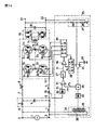
- FIG. 1 is a circuit diagram of a switching power supply device 101 according to a first embodiment of the present invention.
- FIG. 2 shows operation waveforms of main parts of the first embodiment.
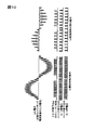
- FIG. 3 shows output voltage waveforms of the switching power supply device of the third conventional example with respect to the AC input voltage and the switching power supply device of the present invention.
- FIG. 4 is a graph showing an example of the relationship between the switching frequency fsw and the output voltage Vout when the voltage Vens across the energy storage capacitor Cens1 is assumed to be a constant value in the first embodiment.
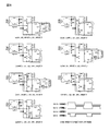
- FIG. 5 is an equivalent circuit in the C mode of the first embodiment of the present invention.
- FIG. 6 is an equivalent circuit in the A1 mode of the first embodiment of the present invention.
- FIG. 7 is an equivalent circuit in the A2 mode of the first embodiment of the present invention.
- FIG. 8 is an equivalent circuit in the B1 mode of the first embodiment of the present invention.
- FIG. 9 is an equivalent circuit in the B2 mode of the first embodiment of the present invention.
- FIG. 10 shows operation waveforms at the time of intermittent switching at light load according to the first embodiment of the present invention.
- FIG. 11 is a circuit diagram of the AC-DC power conversion system 102 of the second embodiment of the present invention.
- FIG. 12 shows an AC-DC power conversion system as a first conventional example.
- FIG. 13 is a circuit diagram of a second conventional example.
- FIG. 14 is a circuit diagram of a third conventional example.
- FIG. 15 is a circuit diagram of a main circuit of a current fed push-pull converter related to the third conventional example.
- FIG. 16 is a circuit diagram of a converter main circuit in which a step-down stage is connected in series with the preceding stage in order to compensate for the drawbacks of the current-fed converter.
- a switching power supply apparatus 101 in the first embodiment of the present invention shown in the circuit diagram of FIG. 1 is a switching power supply apparatus in which a rectification / PFC circuit section and an insulated DC-DC converter section are integrated.
- the rectification / PFC circuit unit is a circuit unit having both the rectification function and the PFC function.
- a PFC inductor Lpfc1 and a bidirectional switch element Qbd are connected in series to the AC power source Acin.
- the PFC inductor Lpfc1 is configured as a transformer having an auxiliary winding for detecting an input current, and the bidirectional switch element Qbd includes a third switch element Q3 and a fourth switch element Q4 that are unidirectional switch elements.
- the third switch element Q3 and the fourth switch element Q4 are N-channel MOSFETs and include a parasitic diode in parallel.
- a first rectifying element D1 having a polarity conducting in the positive half cycle of the AC input voltage, and a second rectifying element D2 having a polarity conducting in the negative half cycle of the AC input voltage Are connected, and a series circuit having a first rectifier element D1 and a first switch element Q1 and a series circuit having a second rectifier element D2 and a second switch element Q2 are the bidirectional switch elements. It is connected in parallel with Qbd.
- An energy storage capacitor Cens1 is connected in parallel with the series switch circuit formed by the first switch element Q1 and the second switch element Q2. Since the energy storage capacitor Cens1 plays a role of supplying energy to the load circuit Load at the time when the AC input voltage decreases or during an instantaneous power failure of the AC input, a relatively large capacity capacitor is required. Since a DC voltage is always applied to the energy storage capacitor Cens1 with the drain side of the first switch element Q1 being (+) and the source side of the second switch element Q2 being (-), an aluminum electrolytic capacitor having polarity is used. I can do things.
- a rectifying and smoothing circuit including a first synchronous rectifying element SR1, a second synchronous rectifying element SR2, and a smoothing capacitor Cf1 is connected to the secondary windings Ns1 and Ns2 of the transformer T1.
- the switching power supply device of the present invention is configured by integrating the rectification / PFC circuit unit and the insulation type DC-DC converter unit.
- the rectification / PFC circuit unit and the insulation type DC-DC converter unit are respectively included independently.
- the output conversion ratio can be controlled. Therefore, the AC ripple generated at both ends of the energy storage capacitor Cens1 is canceled by the control operation of the isolated DC-DC converter unit and is not output from the switching power supply device.
- a high-speed response can be made to the fluctuation of the output voltage by independent control of the isolated DC-DC converter section. Even if an instantaneous power failure occurs, an output voltage holding operation for holding the output voltage value at a specified value for a certain period is possible.
- FIG. 3 is a diagram showing a difference in output voltage between the switching power supply device of the third conventional example with respect to the AC input voltage and the switching power supply device of the present invention, and the AC generated in the switching power supply device of the third conventional example. Ripple does not occur in the switching power supply device of the present invention, and the switching power supply device of the third conventional example cannot perform the output voltage holding operation against the instantaneous power failure, whereas the switching power supply device of the present invention requires the required output voltage. Retention time can be secured. In addition, since there is less conduction loss than the conventional three-stage AC-DC power conversion system shown in FIG. 12, highly efficient power conversion is possible.
- the rectification / PFC circuit unit includes a PFC inductor Lpfc1, a bidirectional switch Qbd, a first rectifier element D1, a second rectifier element D2, a first switch element Q1, a second switch element Q2, and an energy storage capacitor Cens1.
- a PFC inductor Lpfc1 a bidirectional switch Qbd
- the bidirectional switch element Qbd and the first switch element Q1 connected in parallel is a main switch
- the second switch element Q2 is a synchronous rectifier element.
- At least one of the bidirectional switch element Qbd and the second switch element Q2 connected in parallel is a main switch, and the first switch element Q1 is a synchronous rectifier element It functions as a boost converter.
- the boost converter equation is established for the input / output conversion ratio of the rectification / PFC circuit unit, the AC input voltage is defined as Vin, the voltage across the energy storage capacitor is defined as Vens, and in the positive half cycle of the AC input voltage Vin, The ratio of the period when at least one of the bidirectional switch element Qbd and the first switch element Q1 is on to one period, and the negative half period of the AC input voltage Vin, the bidirectional switch element Qbd and the second switch When a ratio of one period of at least one of the elements Q2 to one cycle is defined as a first duty ratio D,
- the insulated DC-DC converter unit includes a first switch element Q1, a second switch element Q2, a resonant inductor Lr1, a resonant capacitor Cr1, a transformer T1, a first synchronous rectifier element SR1, a second synchronous rectifier element SR2, It is composed of a smoothing capacitor Cf1 and a topology called a current resonance converter or LLC resonance converter using the energy storage capacitor Cens1 as a DC input power source.
- the capacitance of the resonant capacitor is Cr
- the inductance of the resonant inductor is Lr
- the exciting inductance of the transformer is Lm
- the input / output voltage conversion ratio of the isolated DC-DC converter unit is the switching frequency fsw
- the first resonance frequency fr1 defined by
- the main switch element is ZVS (zero voltage switching) and the rectifier element is ZCS (zero current switching). is there.
- FIG. 4 shows the relationship between the switching frequency fsw and the output voltage Vout when the first resonance frequency fr1 is set to 480 kHz, the second resonance frequency fr2 is set to 210 kHz, and the voltage Vens across the energy storage capacitor is assumed to be a constant value. It is a graph which shows an example. The resonance of the resonance capacitor Cr, the resonance inductor Lr, and the excitation inductance Lm of the transformer T1 causes the output voltage Vout to increase near the second resonance frequency fr2, and the conversion ratio of the output voltage Vout to the voltage Vens across the energy storage capacitor peaks. Value.
- the output voltage Vout increases or decreases depending on the change of the duty ratio Di, but the duty ratio Di is near the first resonance frequency fr1.
- the impact is relatively small. Therefore, frequency control is performed in a region higher than the second resonance frequency fr2, and when the output voltage Vout is lower than the target value, the switching frequency fsw is lowered to approach the second resonance frequency fr2, and the output voltage Vout is set to the target value. If it is higher, the output voltage Vout can be stabilized with respect to the target voltage value by increasing the switching frequency fsw so as to be away from the second resonance frequency fr2.
- the influence of the duty ratio Di is reduced by setting the switching frequency fsw in the steady operation in the vicinity of the first resonance frequency fr1, and the current resonance converter has the highest efficiency in the vicinity of the first resonance frequency fr1. Since efficient power conversion is possible, highly efficient power conversion operation is also possible.
- the input / output conversion ratio of the rectification / PFC circuit section is controlled independently by PWM (duty ratio) control, and the input / output conversion ratio of the isolated DC-DC converter section is controlled independently by PFM (switching frequency) control. Can do.
- the control circuit shown in the circuit diagram of FIG. 1 is configured.
- the primary side control circuit ground makes it easy to comply with safety standards by setting the AC power supply Acin to a node rectified by the rectifying elements D3 and D4.
- Voltage dividing resistors R1, R2, R3, and R4 are connected between each terminal of the AC power source Acin and the primary side control circuit ground, and the divided voltage is input to the operation mode discriminator Mdt1.
- the operation mode discriminator Mdt1 discriminates the following five types of operation modes according to the range of the AC input voltage Vin, and outputs them to the primary side control circuit CNTP1 as mode discrimination signals (A1, A2, B1, (Refer to each mode of B2 and C).
- the C mode is a period in which the absolute value of the AC input voltage Vin is small and hardly affects the power factor.
- the A1 mode and the A2 mode are periods corresponding to the positive half cycle of the AC input voltage Vin, but the absolute value of the AC input voltage Vin is measured by measuring the absolute value of the AC input voltage Vin from the sine half wave voltage appearing at the voltage dividing points of the resistors R1 and R2. Determine the type of mode. If the absolute value of the AC input voltage Vin is greater than the reference value of the C mode and less than half of the voltage Vens across the energy storage capacitor in the positive half cycle of the AC input voltage Vin, it is determined that the mode is the A1 mode.
- the B1 mode and the B2 mode are periods corresponding to the negative half cycle of the AC input voltage Vin, but the absolute value of the AC input voltage Vin is measured by measuring the absolute value of the AC input voltage Vin from the sine half wave voltage appearing at the voltage dividing points of the resistors R3 and R4. Determine the type of mode. If the absolute value of the AC input voltage Vin is larger than the reference value of the C mode and less than half of the voltage Vens across the energy storage capacitor in the negative half cycle of the AC input voltage Vin, it is determined that the mode is the B1 mode. When the absolute value of the input voltage Vin is larger than 1 ⁇ 2 of the voltage Vens across the energy storage capacitor, it is determined as the B2 mode.
- the second error signal generated by comparing the AC input voltage Vin, the input current, and the voltage Vens across the energy storage capacitor with the reference voltage is generated.
- the AC input voltage Vin can be obtained as a voltage proportional to the AC input voltage Vin from the divided voltages of the resistors R1 and R2 or the resistors R3 and R4.
- the input current is measured by integrating the voltage of the auxiliary winding of the PFC inductor Lpfc1 configured as a transformer by the integration circuit INT1.
- the voltage at each terminal of the energy storage capacitor Cens1 is divided by resistors R5, R6, resistors R7, R8 and input to the fourth comparator AMP4.
- resistors R5, R6, resistors R7, R8 and input to the fourth comparator AMP4 As an example, when the voltage of each terminal of the energy storage capacitor Cens1 is divided by 1/100 with the resistors R5 and R6 and the resistors R7 and R8, the voltage Vens across the energy storage capacitor is between the input terminals of the fourth comparator AMP4. A voltage of 1/100 appears, which is amplified by the fourth comparator AMP4 at a constant magnification, and a voltage proportional to the voltage Vens across the energy storage capacitor is output from the fourth comparator AMP4.
- the output of the fourth comparator AMP4 is compared with the second reference voltage Vref2 by the third comparator AMP3 to generate a second error signal.
- the second error signal is multiplied by a voltage proportional to the AC input voltage Vin obtained from the divided voltage of the resistors R1 and R2 or the resistors R3 and R4 by the multiplier M1, and a signal corresponding to the AC input voltage Vin is obtained. Generated.
- a signal corresponding to the AC input current Vin output from the integrating circuit INT1 and a signal corresponding to the AC input voltage Vin output from the multiplier M1 are compared by the first comparator AMP1, and the first comparator AMP1.
- Dcnt1 To output a second error signal to the duty ratio calculator Dcnt1.
- the duty ratio calculator Dcnt1 includes a voltage proportional to the AC input voltage Vin obtained from the divided voltage of the resistors R1 and R2 or the resistors R3 and R4, and a voltage Vens across the energy storage capacitor from the fourth comparator AMP4. A proportional voltage is input,
- the approximate duty ratio Dr is calculated according to The approximate duty ratio Dr is formed as a feedforward signal, the second error signal is added as a feedback signal to the feedforward signal with a polarity that is negative feedback, and a DC voltage corresponding thereto is supplied from the duty ratio calculator Dcnt1 to the comparator. Output to COMP1.
- a sawtooth wave output from the sawtooth wave generator STG1 is input to the other input of the comparator COMP1, and a square wave signal with the first duty ratio D adjusted is output from the comparator COMP1 to the primary side control circuit CNTP1. Is done.
- the frequency of the sawtooth wave output from the sawtooth wave generator STG1 is modulated by feedback from the output.
- the output voltage Vout is detected by dividing it with resistors R9 and R10, and compared with the first reference voltage Vref1 by the second comparator AMP2, to form a feedback signal.
- the feedback signal is input to the frequency controller Fcnt1 to modulate the frequency of the sawtooth wave.
- the input / output conversion ratio of the isolated DC-DC converter unit is controlled by modulation of the switching frequency.
- the primary-side control circuit CNTP1 includes first, second, third, and fourth switch elements Q1, Q2, Q3, Q4, and first, second, and second switching elements Q1, Q2, and Q4 according to the input square wave signal and the mode determination signal.
- Drive timing signals for the second synchronous rectification elements SR1 and SR2 are generated and output to the first and second insulation signal transmission elements ISO1 and ISO2, respectively.
- the first and second insulation signal transmission elements ISO1 and ISO2 convert the drive timing signal based on the ground of the primary side control circuit into a drive signal based on the source potential of each switch element to convert each switch element. To drive.
- a drive signal is formed so as to provide a dead time during which both of the first switch element Q1 and the second switch element Q2 are turned off between the on period of the first switch element Q1 and the second switch element Q2.
- the on-period of the first synchronous rectifier element SR1 is within the on-period of the second switch element Q2, and the second synchronous rectifier element SR2 is on.
- the period needs to be set within the ON period of the first switch element Q1,
- the current resonance period Trh calculated in (1) is set as the maximum ON period, or the current flowing through the first and second synchronous rectifier elements SR1 and SR2 is detected directly or indirectly to detect a forward current (a predetermined value or more)
- a forward current a predetermined value or more
- the C mode shown in FIG. 5 is a period in which the absolute value of the AC input voltage Vin is small and hardly affects the power factor.
- the third and fourth switch elements Q3 and Q4 are held in an off state in order to save drive loss, and are not shown on the equivalent circuit.
- a current similar to a boost converter in a current discontinuous mode in which the second switch element Q2 is a main switch and the first switch element Q1 is a synchronous rectifier element flows from the AC power supply Acin. small.
- the operation is the same as that of the current resonant converter using the energy storage capacitor Cens1 as an input source.
- the second switch element Q2 and the first synchronous rectifier element SR1 are in an on state, and the first switch element Q1 and the second synchronous rectifier element SR2 are in an off state, which are indicated by arrows.
- a sinusoidal current due to current resonance of the resonance inductor Lr1 and the resonance capacitor Cr1 flows through the path.
- the first synchronous rectifier SR1 is turned off and the operation proceeds to the operation of FIG.
- the second switch element Q2 is in the on state, and the first switch element Q1, the first synchronous rectifier element SR1, and the second synchronous rectifier element SR2 are in the off state, and are indicated by arrows.
- the resonant inductor Lr1, the exciting inductance Lm of the transformer T1, and the resonant current of the resonant capacitor Cr1 flow through the paths.
- the first switch element Q1, the second switch element Q2, the first synchronous rectifier element SR1, and the second synchronous rectifier element SR2 are all in the off state, and the path indicated by the arrows.
- a current flows, and the parasitic capacitance Cdis existing in parallel with the first and second switch elements Q1 and Q2 is charged. If the first switch element Q1 is turned on in a state where the parasitic capacitance Cdis is charged and the voltage across the first switch element Q1 becomes 0V, ZVS (zero voltage switching) is achieved, as shown in FIG. Move to operation.
- the first switch element Q1 and the second synchronous rectifier element SR2 are in an on state, and the second switch element Q2 and the first synchronous rectifier element SR1 are in an off state, which are indicated by arrows.
- a sinusoidal current due to current resonance of the resonance inductor Lr1 and the resonance capacitor Cr1 flows through the path.
- the second synchronous rectifier SR2 is turned off and the operation proceeds to FIG.
- the first switch element Q1 is in an on state
- the second switch element Q2 the first synchronous rectifier element SR1, and the second synchronous rectifier element SR2 are in an off state, indicated by arrows.
- a resonance current flows through the path of the resonance inductor Lr1, the excitation inductance Lm of the transformer T1, and the resonance capacitor Cr1.
- the first switch element Q1, the second switch element Q2, the first synchronous rectifier element SR1, and the second synchronous rectifier element SR2 are all in an off state, and are shown in the path indicated by the arrows.
- a current flows, and the parasitic capacitance Cdis existing in parallel with the first and second switch elements Q1 and Q2 is discharged.
- the second switch element Q2 is turned on in a state where the parasitic capacitance Cdis is discharged and the voltage across the second switch element Q2 becomes 0V, ZVS (zero voltage switching) is achieved, and again FIG. )
- the switching operation is repeated according to the above-described operation.
- the input / output conversion ratio of the isolated DC-DC converter unit is adjusted according to the length of the period corresponding to 5 (b) and FIG. 5 (e).
- the A1 mode shown in FIG. 6 is a positive half cycle of the AC input voltage Vin, when the absolute value of the AC input voltage Vin is larger than the reference value of the C mode and less than 1/2 of the voltage Vens across the energy storage capacitor. Equivalent to.
- the first duty ratio D (duty ratio of the rectification / PFC circuit unit) is PWM controlled within a range of 0.5 or more, but the second duty ratio D 'Is held at 0.5.
- the fourth switch element Q4 functions only as a rectifying element, and therefore is represented as a diode in the equivalent circuit diagram.
- the first switch element Q1, the third switch element Q3, and the second synchronous rectifier element SR2 are in the on state, and the second switch element Q2 and the first synchronous rectifier element SR1 are in the off state.
- the rectification / PFC circuit unit in the A1 mode functions as a boost converter in which the third switch element Q3 forms a main switch and the second switch element Q2 forms a synchronous rectifier element.
- the third switch element Q3 Since is on, the input current gradually increases.
- a sinusoidal current due to current resonance flows through the path of the resonant inductor Lr1 and the resonant capacitor Cr1 indicated by arrows with the energy storage capacitor Cens1 as an input source.
- the second synchronous rectifier SR2 is turned off and the operation proceeds to the operation of FIG.
- the first switch element Q1 and the third switch element Q3 are in the on state, and the second switch element Q2, the first synchronous rectifier element SR1, and the second synchronous rectifier element SR2 are off. State.
- the third switch element Q3 is in the ON state, so that the input current gradually increases. Since the series circuit of the first rectifier element D1 and the first switch element Q1 is connected in parallel with the series circuit of the third and fourth switch elements Q3 and Q4, a part of the current flowing through the PFC inductor Lpfc1 Is shunted to the series circuit of the first rectifying element D1 and the first switching element Q1, and the conduction loss is reduced.
- a resonance current flows through the path of the resonance inductor Lr1, the excitation inductance Lm of the transformer T1, and the resonance capacitor Cr1 indicated by the arrows with the energy storage capacitor Cens1 as an input source.
- the operation of FIG. 6B shifts to the operation of FIG.
- the third switch element Q3 is on, and the first switch element Q1, the second switch element Q2, the first synchronous rectifier element SR1, and the second synchronous rectifier element SR2 are off. State. In the rectification / PFC circuit portion, the third switch element Q3 is in the ON state, so that the input current gradually increases. In the insulated DC-DC converter unit, a current flows through a path indicated by an arrow, and the parasitic capacitance Cdis existing in parallel with the first and second switch elements Q1 and Q2 is discharged. If the second switch element Q2 is turned on in a state in which the parasitic capacitance Cdis is discharged and the voltage across the second switch element Q2 becomes 0V, ZVS (zero voltage switching) is achieved, and FIG. Move to operation.
- the second switch element Q2, the third switch element Q3, and the first synchronous rectifier element SR1 are in the on state, and the first switch element Q1 and the second synchronous rectifier element SR2 are in the off state.
- the third switch element Q3 is in the ON state, so that the input current gradually increases.
- a sinusoidal current due to current resonance flows through the path of the resonant inductor Lr1 and the resonant capacitor Cr1 indicated by arrows.
- the boost converter of the rectification / PFC circuit unit is switched from the on state to the off state, and the operation shifts to the operation of FIG.
- the current of the PFC inductor Lpfc1 gradually decreases while charging the energy storage capacitor Cens1 via the first rectifier element D1 and the second switch element Q2.
- a sinusoidal current due to current resonance flows through the path of the resonant inductor Lr1 and the resonant capacitor Cr1 indicated by arrows.
- the second switch element Q2 has a current flowing from the source to the drain as a synchronous rectifier of the rectification / PFC circuit section, while the primary low side of the isolated DC-DC converter section. A current in the source direction flows from the drain as the switch element.
- the second switch element Q2 is on, and the first switch element Q1, the third switch element Q3, the first synchronous rectifier element SR1, and the second synchronous rectifier element SR2 are off. State.
- the current of the PFC inductor Lpfc1 gradually decreases while charging the energy storage capacitor Cens1 via the first rectifier element D1 and the second switch element Q2.
- a resonance current flows through the path of the resonance capacitor Cr1, the exciting inductance Lm of the transformer T1, the resonance inductor Lr1, and the second switch element Q2 indicated by arrows. Also in the period of FIG.
- the second switch element Q2 has a current flowing from the source to the drain as a synchronous rectifier of the rectification / PFC circuit section, while the primary side of the isolated DC-DC converter section.
- a current in the source direction flows from the drain as the low-side switch element. Since currents in opposite directions cancel each other, the amount of current flowing through the second switch element Q2 is reduced, and conduction loss is reduced.
- the operation shifts to the operation of FIG. 6 (g).
- the boost converter of the rectification / PFC circuit section is switched from the off state to the on state, and the input current gradually increases.
- the first switch element Q1, the second switch element Q2, the first synchronous rectifier element SR1, and the second synchronous rectifier element SR2 are all in an off state, and are indicated by arrows.
- a current flows through the path, and the parasitic capacitance Cdis existing in parallel with the first and second switch elements Q1 and Q2 is charged. If the first switch element Q1 is turned on in a state where the parasitic capacitance Cdis is charged and the voltage across the first switch element Q1 becomes 0V, ZVS is achieved.
- the second duty ratio D ′ is maintained at 0.5, and the first duty ratio D (duty ratio of the rectification / PFC circuit unit) is 0. 0 in order to perform the PFC operation.
- PWM control is performed in a range of 5 or more.
- the input / output conversion ratio of the insulated DC-DC converter unit is adjusted according to the length of the period corresponding to FIGS. 6B and 6F.
- the GS voltage of the fourth switch element Q4 is maintained at a low level (off state). However, since only a parasitic diode is used, the GS voltage is It may be at a high level (on state).
- the A2 mode does not occur in the entire AC input voltage range. For example, when the voltage Vens across the energy storage capacitor is set to 400 V, the A2 mode does not occur when the effective value of the AC voltage is 140 V or less.
- the first duty ratio D (duty ratio of the rectification / PFC circuit unit) is PWM controlled within a range smaller than 0.5, and the second duty ratio is accordingly adjusted.
- D ′ is also substantially equal to the first duty ratio D, and is PWM controlled.
- the fourth switch element Q4 acts only as a rectifying element, and therefore is represented as a diode in the equivalent circuit diagram.
- the first switch element Q1, the third switch element Q3, and the second synchronous rectifier element SR2 are in the on state, and the second switch element Q2 and the first synchronous rectifier element SR1 are in the off state.
- the rectification / PFC circuit unit in the A2 mode functions as a boost converter in which the first switch element Q1 and the third switch element Q3 form a main switch and the second switch element Q2 forms a synchronous rectifier element. ), Since the first switch element Q1 and the third switch element Q3 are in the ON state, the input current gradually increases.
- a sinusoidal current due to current resonance flows through the path of the resonant inductor Lr1 and the resonant capacitor Cr1 indicated by arrows with the energy storage capacitor Cens1 as an input source.
- the second synchronous rectifier SR2 is turned off and the operation proceeds to the operation of FIG.
- the first switch element Q1 and the third switch element Q3 are on, and the second switch element Q2, the first synchronous rectifier element SR1, and the second synchronous rectifier element SR2 are off. State. In the rectification / PFC circuit section, the first switch element Q1 and the third switch element Q3 are in the ON state, so that the input current continues to increase gradually. In FIG. 7B, since the voltage drop due to the current flowing into the first switch element Q1 from the insulated DC-DC converter section is relatively small, a part of the current flowing through the PFC inductor Lpfc1 is the first rectifier element D1. And the first switch element Q1 are shunted to reduce the conduction loss.
- a resonance current flows through the path of the resonance inductor Lr1, the excitation inductance Lm of the transformer T1, and the resonance capacitor Cr1 indicated by the arrows with the energy storage capacitor Cens1 as an input source.
- the operation shown in FIG. 7B is shifted to the operation shown in FIG. 7C.
- the first switch element Q1, the second switch element Q2, the third switch element Q3, the first synchronous rectifier element SR1, and the second synchronous rectifier element SR2 are all in an OFF state.
- the boost converter of the rectification / PFC circuit unit switches from the on state to the off state.
- the parasitic capacitance Cdis existing in parallel with the first and second switch elements Q1 and Q2 is discharged by the current of the PFC inductor Lpfc1 and the current of the path indicated by the arrow of the insulated DC-DC converter unit. If the second switch element Q2 is turned on in a state in which the parasitic capacitance Cdis is discharged and the voltage across the second switch element Q2 becomes 0V, ZVS (zero voltage switching) is achieved, and FIG. Move to operation.
- the second switch element Q2 and the first synchronous rectifier element SR1 are in the on state, and the first switch element Q1, the third switch element Q3, and the second synchronous rectifier element SR2 are off. State.
- the current of the PFC inductor Lpfc1 gradually decreases while charging the energy storage capacitor Cens1 via the first rectifier element D1 and the second switch element Q2.
- a sinusoidal current due to current resonance flows through the path of the resonant inductor Lr1 and the resonant capacitor Cr1 indicated by arrows. In the period of FIG.
- the second switch element Q2 has a current flowing from the source to the drain as a synchronous rectifier element of the rectification / PFC circuit section, while the primary low side of the isolated DC-DC converter section.
- a current in the source direction flows from the drain as the switch element. Since currents in opposite directions cancel each other, the amount of current flowing through the second switch element Q2 is reduced, and conduction loss is reduced.
- the first synchronous rectifying element SR1 is turned off and the operation proceeds to the operation of FIG.
- the second switch element Q2 is in the on state, and the first switch element Q1, the third switch element Q3, the first synchronous rectifier element SR1, and the second synchronous rectifier element SR2 are off. State.
- the current of the PFC inductor Lpfc1 gradually decreases while charging the energy storage capacitor Cens1 via the first rectifier element D1 and the second switch element Q2.
- a resonance current flows through the path of the resonance capacitor Cr1, the exciting inductance Lm of the transformer T1, the resonance inductor Lr1, and the second switch element Q2 indicated by arrows. Even during the period of FIG.
- the second switch element Q2 has a current flowing from the source to the drain as a synchronous rectifier of the rectification / PFC circuit section, while the primary side of the isolated DC-DC converter section.
- a current in the source direction flows from the drain as the low-side switch element. Since currents in opposite directions cancel each other, the amount of current flowing through the second switch element Q2 is reduced, and conduction loss is reduced.
- the third switch element Q3 is in the ON state, and the first switch element Q1, the second switch element Q2, the first synchronous rectifier element SR1, and the second synchronous rectifier element SR2 are Off state. Since the boost converter of the rectification / PFC circuit section switches from the off state to the on state, the input current gradually increases.
- a current flows through a path indicated by an arrow, and the parasitic capacitance Cdis existing in parallel with the first and second switch elements Q1 and Q2 is charged. If the first switch element Q1 is turned on in a state where the parasitic capacitance Cdis is charged and the voltage across the first switch element Q1 becomes 0V, ZVS is achieved.
- the first duty ratio D (duty ratio of the rectification / PFC circuit portion) and the second duty ratio D ′ are substantially the same value, and the first duty ratio D '
- the second duty ratio D ′ is also PWM controlled accordingly.
- the input / output conversion ratio of the insulated DC-DC converter unit is adjusted according to the length of the period corresponding to FIGS. 7B and 7E.
- the GS voltage of the fourth switch element Q4 is maintained at a low level (off state). However, since only a parasitic diode is used, the GS voltage is It may be at a high level (on state).
- the B1 mode shown in FIG. 8 is a negative half cycle of the AC input voltage Vin, and the absolute value of the AC input voltage Vin is larger than the reference value of the C mode and is less than or equal to 1/2 of the voltage Vens across the energy storage capacitor. Equivalent to.
- the circuit operation is similar to that of the A1 mode, but the first rectifier element D1, the second rectifier element D2, the first switch element Q1, the second switch element Q2, the third switch element Q3, The roles of the fourth switch element Q4, the first synchronous rectifier element SR1, and the second synchronous rectifier element SR2 are interchanged.
- the first duty ratio D (duty ratio of the rectification / PFC circuit unit) is PWM controlled within a range of 0.5 or more, but the second duty ratio D 'Is held at 0.5.
- the third switch element Q3 acts only as a rectifying element, and therefore is represented as a diode in the equivalent circuit diagram.
- the second switch element Q2, the fourth switch element Q4, and the first synchronous rectifier element SR1 are on, and the first switch element Q1 and the second synchronous rectifier element SR2 are off.
- the rectification / PFC circuit unit in the B1 mode functions as a boost converter in which the fourth switch element Q4 forms a main switch and the first switch element Q1 forms a synchronous rectifier element.
- the fourth switch element Q4 Since is on, the input current gradually increases.
- a sinusoidal current due to current resonance flows through the path of the resonance capacitor Cr1 and the resonance inductor Lr1 indicated by the arrows.
- the first synchronous rectifying element SR1 is turned off and the operation proceeds to the operation of FIG.
- the second switch element Q2 and the fourth switch element Q4 are in the on state, and the first switch element Q1, the first synchronous rectifier element SR1, and the second synchronous rectifier element SR2 are off. State.
- the fourth switch element Q4 is in the ON state, so that the input current gradually increases. Since the series circuit of the second rectifier element D2 and the second switch element Q2 is connected in parallel with the series circuit of the third and fourth switch elements Q3 and Q4, a part of the current flowing through the PFC inductor Lpfc1 Is shunted to the series circuit of the second rectifier element D2 and the second switch element Q2, and the conduction loss is reduced.
- the fourth switch element Q4 is in the on state, and the first switch element Q1, the second switch element Q2, the first synchronous rectifier element SR1, and the second synchronous rectifier element SR2 are off. State. In the rectification / PFC circuit portion, the fourth switch element Q4 is in the ON state, so that the input current gradually increases. In the insulated DC-DC converter unit, a current flows through a path indicated by an arrow, and the parasitic capacitance Cdis existing in parallel with the first and second switch elements Q1 and Q2 is charged. If the first switch element Q1 is turned on in a state where the parasitic capacitance Cdis is charged and the voltage across the first switch element Q1 becomes 0V, ZVS (zero voltage switching) is achieved, as shown in FIG. Move to operation.
- the first switch element Q1, the fourth switch element Q4, and the second synchronous rectifier element SR2 are on, and the second switch element Q2 and the first synchronous rectifier element SR1 are off.
- the fourth switch element Q4 is in the ON state, so that the input current gradually increases.
- a sinusoidal current due to current resonance flows through the path of the resonant inductor Lr1 and the resonant capacitor Cr1 indicated by arrows with the energy storage capacitor Cens1 as an input source.
- the boost converter of the rectification / PFC circuit unit is switched from the on state to the off state, and the operation shifts to the operation of FIG.
- the current of the PFC inductor Lpfc1 gradually decreases while charging the energy storage capacitor Cens1 via the second rectifier element D2 and the first switch element Q1.
- a sine wave current due to current resonance flows through the path of the resonant inductor Lr1 and the resonant capacitor Cr1 indicated by arrows using the energy storage capacitor Cens1 as an input source.
- the first switch element Q1 has a current flowing from the source to the drain as a synchronous rectifier element of the rectification / PFC circuit section, while the primary side of the isolated DC-DC converter section is high. A current in the source direction flows from the drain as the side switch element.
- the first switch element Q1 is in the on state, and the second switch element Q2, the fourth switch element Q4, the first synchronous rectifier element SR1, and the second synchronous rectifier element SR2 are off. State.
- the current of the PFC inductor Lpfc1 continues to gradually decrease while charging the energy storage capacitor Cens1 via the second rectifier element D2 and the first switch element Q1.
- a resonance current flows through the path of the first switching element Q1, the resonance inductor Lr1, the excitation inductance Lm of the transformer T1, and the resonance capacitor Cr1 indicated by arrows using the energy storage capacitor Cens1 as an input source. . Also in the period of FIG.
- the first switch element Q1 has a current flowing from the source to the drain as a synchronous rectifier of the rectification / PFC circuit section, while the primary side of the isolated DC-DC converter section.
- a current in the source direction flows from the drain. Since currents in opposite directions cancel each other, the amount of current flowing through the first switch element Q1 is reduced, and conduction loss is reduced.
- FIG. 8F when the first switch element Q1 is turned off and the fourth switch element Q4 is turned on, the operation shown in FIG. 8G is started.
- the boost converter of the rectification / PFC circuit section is switched from the off state to the on state, and the input current gradually increases.
- the first switch element Q1, the second switch element Q2, the first synchronous rectifier element SR1, and the second synchronous rectifier element SR2 are all in an off state, and are indicated by arrows.
- a current flows through the path, and the parasitic capacitance Cdis existing in parallel with the first and second switch elements Q1 and Q2 is discharged. If the second switch element Q2 is turned on in a state where the parasitic capacitance Cdis is discharged and the voltage across the second switch element Q2 becomes 0V, ZVS is achieved.
- the second duty ratio D ′ is held at 0.5, and the first duty ratio D (duty ratio of the rectification / PFC circuit unit) is set to 0. 0 to perform the PFC operation.
- PWM control is performed in a range of 5 or more.
- the input / output conversion ratio of the isolated DC-DC converter unit is adjusted according to the length of the period corresponding to FIGS. 8B and 8F.
- the GS voltage of the third switch element Q3 is maintained at a low level (off state). However, since only a parasitic diode is used, the GS voltage is It may be at a high level (on state).
- the B2 mode shown in FIG. 9 corresponds to a case where the negative half cycle of the AC input voltage Vin and the absolute value of the AC input voltage Vin is larger than 1 ⁇ 2 of the voltage Vens across the energy storage capacitor.
- the first duty ratio D (duty ratio of the rectification / PFC circuit unit) is PWM controlled within a range smaller than 0.5, and the second duty ratio is accordingly adjusted.
- D ′ is also substantially equal to the first duty ratio D, and is PWM controlled.
- the circuit operation is similar to the A2 mode, but the first rectifier element D1, the second rectifier element D2, the first switch element Q1, the second switch element Q2, the third switch element Q3, The roles of the fourth switch element Q4, the first synchronous rectifier element SR1, and the second synchronous rectifier element SR2 are interchanged.
- the third switching element Q3 acts only as a rectifying element, and therefore is represented as a diode in the equivalent circuit diagram.
- the B2 mode does not occur in the entire AC input voltage range. For example, when the voltage Vens across the energy storage capacitor is set to 400 V, the B2 mode does not occur if the effective value of the AC voltage is 140 V or less.
- the second switch element Q2, the fourth switch element Q4, and the first synchronous rectifier element SR1 are on, and the first switch element Q1 and the second synchronous rectifier element SR2 are off.
- the rectification / PFC circuit section in the B2 mode functions as a boost converter in which the second switch element Q2 and the fourth switch element Q4 form a main switch and the first switch element Q1 forms a synchronous rectifier element. ) Since the second switch element Q2 and the fourth switch element Q4 are in the ON state, the input current gradually increases.
- a sinusoidal current due to current resonance flows through the path of the resonant inductor Lr1 and the resonant capacitor Cr1 indicated by arrows.
- the first synchronous rectifier SR1 is turned off and the operation proceeds to the operation of FIG.
- the second switch element Q2 and the fourth switch element Q4 are in the on state, and the first switch element Q1, the first synchronous rectifier element SR1, and the second synchronous rectifier element SR2 are off. State. In the rectification / PFC circuit section, the second switch element Q2 and the fourth switch element Q4 are in the ON state, so that the input current continues to increase gradually. In FIG. 9B, since the voltage drop due to the current flowing into the second switch element Q2 from the insulated DC-DC converter portion is relatively small, a part of the current flowing through the PFC inductor Lpfc1 is the second rectifier element D2. And the second switch element Q2 are shunted to reduce the conduction loss.
- the first switch element Q1, the second switch element Q2, the fourth switch element Q4, the first synchronous rectifier element SR1, and the second synchronous rectifier element SR2 are all in the OFF state.
- the boost converter of the rectification / PFC circuit unit switches from the on state to the off state.
- the parasitic capacitance Cdis existing in parallel with the first and second switch elements Q1 and Q2 is charged by the current of the PFC inductor Lpfc1 and the current of the path indicated by the arrow of the insulated DC-DC converter section. If the first switch element Q1 is turned on in a state where the parasitic capacitance Cdis is charged and the voltage across the first switch element Q1 becomes 0V, ZVS (zero voltage switching) is achieved, as shown in FIG. Move to operation.
- the first switch element Q1 and the second synchronous rectifier element SR2 are on, and the second switch element Q2, the fourth switch element Q4, and the first synchronous rectifier element SR1 are off. State.
- the current of the PFC inductor Lpfc1 gradually decreases while charging the energy storage capacitor Cens1 via the second rectifier element D2 and the first switch element Q1.
- a sinusoidal current due to current resonance flows through the path of the resonant inductor Lr1 and the resonant capacitor Cr1 indicated by arrows with the energy storage capacitor Cens1 as an input source. In the period of FIG.
- the first switch element Q1 has a current flowing from the source to the drain as a synchronous rectifier element of the rectification / PFC circuit section, while the primary side of the isolated DC-DC converter section is high.
- a current in the source direction flows from the drain as the side switch element. Since currents in opposite directions cancel each other, the amount of current flowing through the first switch element Q1 is reduced, and conduction loss is reduced.
- the second synchronous rectifier SR2 is turned off and the operation proceeds to the operation of FIG.
- the first switch element Q1 is in the on state, and the second switch element Q2, the fourth switch element Q4, the first synchronous rectifier element SR1, and the second synchronous rectifier element SR2 are off. State.
- the current of the PFC inductor Lpfc1 continues to gradually decrease while charging the energy storage capacitor Cens1 via the second rectifier element D2 and the first switch element Q1.
- the resonance current is supplied to the path of the first switch element Q1, the resonant inductor Lr1, the exciting inductance Lm of the transformer T1, and the resonant capacitor Cr1 indicated by the arrows with the energy storage capacitor Cens1 as an input source. Flowing. Also in the period of FIG.
- the first switch element Q1 has a current flowing from the source to the drain as a synchronous rectifier of the rectification / PFC circuit section, while the primary side of the isolated DC-DC converter section.
- a current in the source direction flows from the drain. Since currents in opposite directions cancel each other, the amount of current flowing through the first switch element Q1 is reduced, and conduction loss is reduced.
- the operation shifts to the operation of FIG. 9 (f).
- the fourth switch element Q4 is in the ON state, and the first switch element Q1, the second switch element Q2, the first synchronous rectifier element SR1, and the second synchronous rectifier element SR2 are Off state. Since the boost converter of the rectification / PFC circuit section switches from the off state to the on state, the input current gradually increases.
- a current flows through a path indicated by an arrow, and the parasitic capacitance Cdis existing in parallel with the first and second switch elements Q1 and Q2 is discharged. If the second switch element Q2 is turned on in a state where the parasitic capacitance Cdis is discharged and the voltage across the second switch element Q2 becomes 0V, ZVS is achieved.
- the first duty ratio D (duty ratio of the rectification / PFC circuit portion) and the second duty ratio D ′ are substantially the same value, and the first duty ratio D '
- the second duty ratio D ′ is also PWM controlled accordingly.
- the input / output conversion ratio of the insulated DC-DC converter unit is adjusted according to the length of the period corresponding to FIGS. 9B and 9E.
- the GS voltage of the third switch element Q3 is maintained at a low level (off state), but since only a parasitic diode is used, the GS voltage is It may be at a high level (on state).
- FIG. 10 shows a waveform of intermittent operation in the light load region of the switching power supply device of the first embodiment.
- the first switch element Q1 and the second switch element Q2 are continuously driven at a complementary timing with a dead time when both are turned off.
- the bidirectional switch element Qbd (configured by a series circuit in which the third switch element Q3 and the fourth switch element Q4 are connected in the reverse direction) is also continuously switched in the region excluding the C mode.
- the current flowing through the PFC inductor Lpfc1 is in a continuous mode, and it is possible to obtain a substantially sinusoidal input current waveform as shown by a dotted line simply by providing a simple input filter.
- the switching power supply of the first embodiment can reduce the output voltage Vout below the target value by reducing the duty ratio of the switch element corresponding to the main switch of the boost converter or by increasing the switching frequency. Therefore, it can support soft start operation and drooping operation of output voltage against overcurrent. Further, even if the switching operation is stopped during the operation, no surge voltage is generated at both ends of the switch element and the rectifying element, so that it can be stopped without any problem.
- the switching power supply device of the first embodiment has the following features suitable for highly efficient power conversion in addition to the above.
- the current resonance converter that constitutes the isolated DC-DC converter can perform the most efficient power conversion when the duty ratio is 0.5, but the AC-DC power conversion system is combined into one stage. Nevertheless, the ratio of the period during which the duty ratio of the isolated DC-DC converter section can be maintained at 0.5 is large. As an example, when the voltage Vens across the energy storage capacitor is set to 400 V, the duty ratio is set to 0.5% over the entire period when the effective value of the AC voltage is 240 V and when the effective value of the AC voltage is 140 V or less. Can be retained. In the AC-DC power conversion system, the efficiency tends to decrease when the effective value of the AC voltage is low. However, the switching power supply device of the first embodiment is a low voltage that can maintain the duty ratio at 0.5 over the entire period. The effect of improving the efficiency is particularly great at the input, and heat dissipation of the power conversion component is facilitated.
- MOSFET parasitic diodes useful for the first and second switching elements generally tend to have poor reverse recovery characteristics than commercially available high-speed diodes.
- the switching power supply of the first embodiment the following It doesn't matter for a reason.
- the parasitic diode is generated by the reverse current flowing from the isolated DC-DC converter. The amount of current that is conducted decreases.
- the gate signal is applied to the first switch element Q1 or the second switch element Q2. In this state, the amount of current that conducts the parasitic diode portion is small.
- Reverse recovery current can be prevented by using high-speed diodes having excellent reverse recovery characteristics for the first rectifying element D1 and the second rectifying element D2 connected in series.
- the output voltage can be reduced to around 0V, it is possible to perform drooping operation or soft start operation of the output voltage against overcurrent.
- the output ripple is small, and it is possible to maintain a high-speed response to a sudden change and an output voltage against an instantaneous power failure.
- ⁇ ⁇ Input filter can be simplified because the input current is in continuous current mode in most areas.
- an AC input / DC output power conversion system constituted by three stages in the first conventional example and two stages in the second conventional example can be constituted by only one stage as in the third conventional example. Since the circuit configuration is small and the circuit configuration is simple, it is advantageous for downsizing and cost reduction.
- the synchronous rectifying element of the rectification / PFC circuit part also functions as a primary side switching element of the isolated DC-DC converter part, and currents in opposite directions cancel each other and decrease, so that there is little conduction loss.
- the series circuit of the first rectifier element D1 and the first switch element Q1, or the second rectifier element D2 and the second In the operating state where the current of the bidirectional switch element Qbd is large and the current of the parallel circuit is small, the current of the bidirectional switch element Qbd is shunted to the parallel circuit. Can be reduced.
- the ratio of the period during which the duty ratio of the insulated DC-DC converter can be maintained at 0.5, which is the most efficient, is large.
- the low-speed reverse recovery characteristics of the parasitic diodes of the MOSFETs constituting the first and second switch elements are not a problem.
- FIG. 11 is a circuit diagram of the AC-DC power conversion system 102 in the second embodiment of the present invention, which is an example in which the present invention is applied to a three-phase AC, and is supplied from a three-phase AC power supply ACin3P by a ⁇ connection.
- a total of three switching power supply devices of the present invention already shown in the first embodiment are connected between the phases for the phase alternating current.
- the circuit configuration shown in the first embodiment can be used, and if a total of three switching power supply devices are connected between the phases, the output is as efficient as the first embodiment.
- the ripple is small, and it is possible to secure a high-speed response and a holding time for an instantaneous input power failure.
- the control and switching operations in the primary side control circuits CNTP1, CNTP2, and CNTP3 of each switching power supply are substantially the same as those in the first embodiment.
- the secondary side control circuits CNTS1, CNTS2, and CNTS3 of each switching power supply unit obtain the average value of the secondary coil voltage drop by measuring and integrating the voltages across the secondary coils of the transformers T1, T2, and T3. Since the average value of the secondary coil voltage drop is substantially proportional to the output current, an output current signal correlating with the output current of each switching power supply device is obtained.
- Each switching power supply device exchanges output current signals in the current balance circuit Cshare, and a switching power supply device with less output current sharing can balance the output current by automatically adjusting the output voltage to slightly increase. By balancing the output currents of the switching power supply devices, the three-phase AC input current can be balanced as a result.
- the second embodiment has the following effects in addition to the effects of the first embodiment.
- a switching power supply device having a current balance function is configured, a single-phase AC switching power supply device can be used as it is to construct a three-phase AC-DC power conversion system.
- one PFC inductor is connected to each switching power supply, but it may be divided into two and inserted into both AC input lines. Bidirectional power transmission is also possible if the first and second rectifying elements are composed of synchronous rectifying elements. It is also possible to combine the PFC inductor Lpfc1 and the transformer T1 into a single magnetic component using a technique disclosed in Japanese Patent Laid-Open No. 2000-260639. The control method is not limited to the methods of the first and second embodiments. A current detection resistor or a current transformer may be used to detect the input current.
- the feedback control may be used to determine the duty ratio of each switch element.
- the output voltage may be stabilized by frequency control with a duty ratio fixed to a value other than 0.5, for example, 0.2 or 0.8.
- A2 mode AC input B1 mode with a positive half cycle of the voltage Vin and the absolute value of the AC input voltage Vin being greater than 1/2 of the voltage Vens across the energy storage capacitor .... A negative half cycle of the AC input voltage Vin and an AC input.
- the absolute value of the voltage Vin is greater than or equal to the reference value of the C mode and less than 1/2 of the voltage Vens across the energy storage capacitor.
- ⁇ C mode with negative half cycle of AC input voltage Vin and the absolute value of AC input voltage Vin is larger than 1/2 of the voltage Vens across the energy storage capacitor:
- the absolute value of AC input voltage Vin is less than the reference value Dcnt1 ...
Landscapes
- Engineering & Computer Science (AREA)
- Power Engineering (AREA)
- Rectifiers (AREA)
- Dc-Dc Converters (AREA)
Abstract
La présente invention concerne une source d'alimentation électrique à commutation ne comportant qu'un seul étage, à haut rendement et assurant une fonction de maintien de tension de sortie de façon à répondre à des pannes de courant instantanées. Sur le demi-cycle positif d'une tension d'entrée de courant alternatif, une première partie de circuit de redressement/PFC est formée à partir d'un élément de commutation bidirectionnelle (Qbd) ou d'un premier élément de commutation (Q1), d'un second élément de commutation (Q2) et d'un condensateur d'accumulation d'énergie (Cens1). Sur le demi-cycle négatif de tension d'entrée de courant alternatif, une seconde partie de circuit de redressement/PFC est formée à partir de l'élément de commutation bidirectionnelle (Qbd) ou du second élément de commutation (Q2), du premier élément de commutation (Q1) et du condensateur d'accumulation d'énergie (Cens1). Des circuits résonants en série sont connectés au niveau du point de connexion du premier élément de commutation (Q1) et du second élément de commutation (Q2), en configurant un convertisseur cc-cc de type à isolation comportant le condensateur d'accumulation d'énergie (Cens1) en tant que source d'alimentation d'entrée.
Priority Applications (1)
| Application Number | Priority Date | Filing Date | Title |
|---|---|---|---|
| JP2014558537A JP5790889B2 (ja) | 2013-01-22 | 2014-01-15 | スイッチング電源装置およびac−dc電力変換システム |
Applications Claiming Priority (2)
| Application Number | Priority Date | Filing Date | Title |
|---|---|---|---|
| JP2013-009538 | 2013-01-22 | ||
| JP2013009538 | 2013-01-22 |
Publications (1)
| Publication Number | Publication Date |
|---|---|
| WO2014115618A1 true WO2014115618A1 (fr) | 2014-07-31 |
Family
ID=51227410
Family Applications (1)
| Application Number | Title | Priority Date | Filing Date |
|---|---|---|---|
| PCT/JP2014/050562 Ceased WO2014115618A1 (fr) | 2013-01-22 | 2014-01-15 | Source d'alimentation électrique à commutation et système de conversion de courant alternatif en courant continu |
Country Status (2)
| Country | Link |
|---|---|
| JP (1) | JP5790889B2 (fr) |
| WO (1) | WO2014115618A1 (fr) |
Cited By (10)
| Publication number | Priority date | Publication date | Assignee | Title |
|---|---|---|---|---|
| JP6026049B2 (ja) * | 2014-11-11 | 2016-11-16 | 三菱電機株式会社 | 電力変換装置 |
| KR101877019B1 (ko) * | 2018-02-13 | 2018-07-10 | 스마트론파워(주) | 영전압 스위칭을 위한 스마트 턴온 방식의 llc 컨버터 |
| KR20190097819A (ko) * | 2018-02-13 | 2019-08-21 | 스마트론파워(주) | 영전압 스위칭을 위한 스마트 턴온 방식의 llc 컨버터 |
| TWI678874B (zh) * | 2018-09-19 | 2019-12-01 | 宏碁股份有限公司 | 可提升功率因素的電源供應電路 |
| JP2020036421A (ja) * | 2018-08-28 | 2020-03-05 | キヤノン株式会社 | 電源装置及び画像形成装置 |
| TWI726759B (zh) * | 2020-07-01 | 2021-05-01 | 宏碁股份有限公司 | 改良輸出穩定度之升壓轉換器 |
| CN114640262A (zh) * | 2022-05-16 | 2022-06-17 | 广东希荻微电子股份有限公司 | 电压转换电路与电子设备 |
| CN115800749A (zh) * | 2021-09-10 | 2023-03-14 | 深圳快芯半导体技术有限公司 | 一种正反激有源钳位驱动电路 |
| TWI890572B (zh) * | 2024-08-26 | 2025-07-11 | 亞源科技股份有限公司 | 應用於直流電源轉換器之混模操作方法 |
| WO2025213360A1 (fr) * | 2024-04-09 | 2025-10-16 | 华为技术有限公司 | Procédé de commande de tension, appareil de stabilisation de puissance et dispositif |
Families Citing this family (1)
| Publication number | Priority date | Publication date | Assignee | Title |
|---|---|---|---|---|
| KR101854630B1 (ko) * | 2017-09-13 | 2018-05-03 | 주식회사 인터엠 | 앰프용 스위칭 모드 파워 서플라이를 위한 단락 보호 기법 |
Citations (4)
| Publication number | Priority date | Publication date | Assignee | Title |
|---|---|---|---|---|
| JPH11356047A (ja) * | 1998-06-08 | 1999-12-24 | Cosel Co Ltd | スイッチングレギュレータ電源装置 |
| JP2008048487A (ja) * | 2006-08-11 | 2008-02-28 | Toyota Industries Corp | 交流直流変換装置、および交流直流変換装置の駆動方法 |
| JP2008283818A (ja) * | 2007-05-11 | 2008-11-20 | Nanao Corp | スイッチング電源装置 |
| JP2013021861A (ja) * | 2011-07-13 | 2013-01-31 | Sanken Electric Co Ltd | 電源装置及びその制御方法 |
-
2014
- 2014-01-15 WO PCT/JP2014/050562 patent/WO2014115618A1/fr not_active Ceased
- 2014-01-15 JP JP2014558537A patent/JP5790889B2/ja active Active
Patent Citations (4)
| Publication number | Priority date | Publication date | Assignee | Title |
|---|---|---|---|---|
| JPH11356047A (ja) * | 1998-06-08 | 1999-12-24 | Cosel Co Ltd | スイッチングレギュレータ電源装置 |
| JP2008048487A (ja) * | 2006-08-11 | 2008-02-28 | Toyota Industries Corp | 交流直流変換装置、および交流直流変換装置の駆動方法 |
| JP2008283818A (ja) * | 2007-05-11 | 2008-11-20 | Nanao Corp | スイッチング電源装置 |
| JP2013021861A (ja) * | 2011-07-13 | 2013-01-31 | Sanken Electric Co Ltd | 電源装置及びその制御方法 |
Cited By (14)
| Publication number | Priority date | Publication date | Assignee | Title |
|---|---|---|---|---|
| JP6026049B2 (ja) * | 2014-11-11 | 2016-11-16 | 三菱電機株式会社 | 電力変換装置 |
| KR102446692B1 (ko) | 2018-02-13 | 2022-09-27 | 스마트론파워(주) | 영전압 스위칭을 위한 스마트 턴온 방식의 llc 컨버터 |
| KR101877019B1 (ko) * | 2018-02-13 | 2018-07-10 | 스마트론파워(주) | 영전압 스위칭을 위한 스마트 턴온 방식의 llc 컨버터 |
| KR20190097819A (ko) * | 2018-02-13 | 2019-08-21 | 스마트론파워(주) | 영전압 스위칭을 위한 스마트 턴온 방식의 llc 컨버터 |
| JP7166843B2 (ja) | 2018-08-28 | 2022-11-08 | キヤノン株式会社 | 電源装置及び画像形成装置 |
| JP2020036421A (ja) * | 2018-08-28 | 2020-03-05 | キヤノン株式会社 | 電源装置及び画像形成装置 |
| TWI678874B (zh) * | 2018-09-19 | 2019-12-01 | 宏碁股份有限公司 | 可提升功率因素的電源供應電路 |
| US10498223B1 (en) | 2018-09-19 | 2019-12-03 | Acer Incorporated | Power supply circuit with improved power factor |
| TWI726759B (zh) * | 2020-07-01 | 2021-05-01 | 宏碁股份有限公司 | 改良輸出穩定度之升壓轉換器 |
| CN115800749A (zh) * | 2021-09-10 | 2023-03-14 | 深圳快芯半导体技术有限公司 | 一种正反激有源钳位驱动电路 |
| CN114640262A (zh) * | 2022-05-16 | 2022-06-17 | 广东希荻微电子股份有限公司 | 电压转换电路与电子设备 |
| US11750093B1 (en) | 2022-05-16 | 2023-09-05 | Halo Microelectronics Co., Ltd. | Voltage conversion circuits and electronic equipment |
| WO2025213360A1 (fr) * | 2024-04-09 | 2025-10-16 | 华为技术有限公司 | Procédé de commande de tension, appareil de stabilisation de puissance et dispositif |
| TWI890572B (zh) * | 2024-08-26 | 2025-07-11 | 亞源科技股份有限公司 | 應用於直流電源轉換器之混模操作方法 |
Also Published As
| Publication number | Publication date |
|---|---|
| JPWO2014115618A1 (ja) | 2017-01-26 |
| JP5790889B2 (ja) | 2015-10-07 |
Similar Documents
| Publication | Publication Date | Title |
|---|---|---|
| JP5790889B2 (ja) | スイッチング電源装置およびac−dc電力変換システム | |
| JP5757344B2 (ja) | スイッチング電源装置およびac−dc電力変換システム | |
| JP5704124B2 (ja) | スイッチング電源装置 | |
| US8842450B2 (en) | Power converter using multiple phase-shifting quasi-resonant converters | |
| JP5530401B2 (ja) | 電源装置 | |
| CN104883082B (zh) | 电力变换装置 | |
| CN108539984B (zh) | 开关电源电路的pfwm控制系统 | |
| JP4232845B1 (ja) | 直流変換装置 | |
| WO2019206067A1 (fr) | Alimentation à découpage | |
| JP2015144554A (ja) | 電力変換装置 | |
| JP2015208171A (ja) | 電源装置 | |
| JP2008289228A (ja) | 電力変換装置 | |
| WO2015106643A1 (fr) | Circuit dévolteur sans pont de correction du facteur de puissance active (apfc) | |
| TW201436444A (zh) | 交流-直流功率轉換器 | |
| CN103683946A (zh) | 具功率因数校正与脉宽调变机制的电源供应装置及其方法 | |
| CN102668352B (zh) | 带有功率因数校正的转换器 | |
| JP2015042080A (ja) | スイッチング電源装置 | |
| CN114499240A (zh) | 功率转换装置 | |
| US9755504B2 (en) | Flux converter with power factor correction | |
| TWI551024B (zh) | 交流-直流電力轉換裝置及其控制方法 | |
| JP2017163657A (ja) | 電力変換装置 | |
| JP6048150B2 (ja) | 絶縁型スイッチング電源装置 | |
| JP5608181B2 (ja) | 電力変換装置 | |
| JP5577933B2 (ja) | コンバータ | |
| CN105991031B (zh) | 一种电压转换电路、开关电源及电压转换方法 |
Legal Events
| Date | Code | Title | Description |
|---|---|---|---|
| 121 | Ep: the epo has been informed by wipo that ep was designated in this application |
Ref document number: 14743503 Country of ref document: EP Kind code of ref document: A1 |
|
| ENP | Entry into the national phase |
Ref document number: 2014558537 Country of ref document: JP Kind code of ref document: A |
|
| NENP | Non-entry into the national phase |
Ref country code: DE |
|
| 122 | Ep: pct application non-entry in european phase |
Ref document number: 14743503 Country of ref document: EP Kind code of ref document: A1 |