WO2014119206A1 - 温度センサ - Google Patents
温度センサ Download PDFInfo
- Publication number
- WO2014119206A1 WO2014119206A1 PCT/JP2013/084768 JP2013084768W WO2014119206A1 WO 2014119206 A1 WO2014119206 A1 WO 2014119206A1 JP 2013084768 W JP2013084768 W JP 2013084768W WO 2014119206 A1 WO2014119206 A1 WO 2014119206A1
- Authority
- WO
- WIPO (PCT)
- Prior art keywords
- insulating film
- pair
- thermistor
- thin film
- temperature sensor
- Prior art date
- Legal status (The legal status is an assumption and is not a legal conclusion. Google has not performed a legal analysis and makes no representation as to the accuracy of the status listed.)
- Ceased
Links
Images







Classifications
-
- G—PHYSICS
- G01—MEASURING; TESTING
- G01K—MEASURING TEMPERATURE; MEASURING QUANTITY OF HEAT; THERMALLY-SENSITIVE ELEMENTS NOT OTHERWISE PROVIDED FOR
- G01K7/00—Measuring temperature based on the use of electric or magnetic elements directly sensitive to heat ; Power supply therefor, e.g. using thermoelectric elements
- G01K7/16—Measuring temperature based on the use of electric or magnetic elements directly sensitive to heat ; Power supply therefor, e.g. using thermoelectric elements using resistive elements
- G01K7/22—Measuring temperature based on the use of electric or magnetic elements directly sensitive to heat ; Power supply therefor, e.g. using thermoelectric elements using resistive elements the element being a non-linear resistance, e.g. thermistor
-
- G—PHYSICS
- G01—MEASURING; TESTING
- G01K—MEASURING TEMPERATURE; MEASURING QUANTITY OF HEAT; THERMALLY-SENSITIVE ELEMENTS NOT OTHERWISE PROVIDED FOR
- G01K1/00—Details of thermometers not specially adapted for particular types of thermometer
- G01K1/14—Supports; Fastening devices; Arrangements for mounting thermometers in particular locations
- G01K1/143—Supports; Fastening devices; Arrangements for mounting thermometers in particular locations for measuring surface temperatures
-
- G—PHYSICS
- G01—MEASURING; TESTING
- G01K—MEASURING TEMPERATURE; MEASURING QUANTITY OF HEAT; THERMALLY-SENSITIVE ELEMENTS NOT OTHERWISE PROVIDED FOR
- G01K13/00—Thermometers specially adapted for specific purposes
- G01K13/04—Thermometers specially adapted for specific purposes for measuring temperature of moving solid bodies
- G01K13/08—Thermometers specially adapted for specific purposes for measuring temperature of moving solid bodies in rotary movement
-
- H—ELECTRICITY
- H01—ELECTRIC ELEMENTS
- H01C—RESISTORS
- H01C1/00—Details
- H01C1/14—Terminals or tapping points specially adapted for resistors; Arrangements of terminals or tapping points on resistors
-
- H—ELECTRICITY
- H01—ELECTRIC ELEMENTS
- H01C—RESISTORS
- H01C1/00—Details
- H01C1/14—Terminals or tapping points specially adapted for resistors; Arrangements of terminals or tapping points on resistors
- H01C1/1406—Terminals or electrodes formed on resistive elements having positive temperature coefficient
-
- H—ELECTRICITY
- H01—ELECTRIC ELEMENTS
- H01C—RESISTORS
- H01C1/00—Details
- H01C1/14—Terminals or tapping points specially adapted for resistors; Arrangements of terminals or tapping points on resistors
- H01C1/1413—Terminals or electrodes formed on resistive elements having negative temperature coefficient
-
- H—ELECTRICITY
- H01—ELECTRIC ELEMENTS
- H01C—RESISTORS
- H01C1/00—Details
- H01C1/14—Terminals or tapping points specially adapted for resistors; Arrangements of terminals or tapping points on resistors
- H01C1/142—Terminals or tapping points specially adapted for resistors; Arrangements of terminals or tapping points on resistors the terminals or tapping points being coated on the resistive element
-
- H—ELECTRICITY
- H01—ELECTRIC ELEMENTS
- H01C—RESISTORS
- H01C7/00—Non-adjustable resistors formed as one or more layers or coatings; Non-adjustable resistors made from powdered conducting material or powdered semi-conducting material with or without insulating material
- H01C7/006—Thin film resistors
-
- H—ELECTRICITY
- H01—ELECTRIC ELEMENTS
- H01C—RESISTORS
- H01C7/00—Non-adjustable resistors formed as one or more layers or coatings; Non-adjustable resistors made from powdered conducting material or powdered semi-conducting material with or without insulating material
- H01C7/008—Thermistors
-
- H—ELECTRICITY
- H01—ELECTRIC ELEMENTS
- H01C—RESISTORS
- H01C7/00—Non-adjustable resistors formed as one or more layers or coatings; Non-adjustable resistors made from powdered conducting material or powdered semi-conducting material with or without insulating material
- H01C7/04—Non-adjustable resistors formed as one or more layers or coatings; Non-adjustable resistors made from powdered conducting material or powdered semi-conducting material with or without insulating material having negative temperature coefficient
-
- H—ELECTRICITY
- H10—SEMICONDUCTOR DEVICES; ELECTRIC SOLID-STATE DEVICES NOT OTHERWISE PROVIDED FOR
- H10N—ELECTRIC SOLID-STATE DEVICES NOT OTHERWISE PROVIDED FOR
- H10N10/00—Thermoelectric devices comprising a junction of dissimilar materials, i.e. devices exhibiting Seebeck or Peltier effects
- H10N10/80—Constructional details
-
- H—ELECTRICITY
- H10—SEMICONDUCTOR DEVICES; ELECTRIC SOLID-STATE DEVICES NOT OTHERWISE PROVIDED FOR
- H10W—GENERIC PACKAGES, INTERCONNECTIONS, CONNECTORS OR OTHER CONSTRUCTIONAL DETAILS OF DEVICES COVERED BY CLASS H10
- H10W70/00—Package substrates; Interposers; Redistribution layers [RDL]
- H10W70/40—Leadframes
Definitions
- the present invention relates to a temperature sensor suitable for measuring the temperature of a heating roller such as a copying machine or a printer.
- a temperature sensor is installed in contact with a heating roller used in a copying machine or printer in order to measure its temperature.
- a temperature sensor for example, in Patent Documents 1 and 2, a pair of lead frames, a thermal element disposed and connected between the lead frames, and an end portion of the pair of lead frames are formed.
- a temperature sensor having a holding portion and a thin film sheet that is provided on one surface of a lead frame and a thermal element and is brought into contact with a heating roller.
- Such a temperature sensor is brought into contact with the surface of the heating roller using the elastic force of the lead frame to detect the temperature.
- a bead thermistor or a chip thermistor is employed as the thermal element
- a thin film thermistor in which a thermal film is formed on one surface of an insulating substrate such as alumina as the thermal element Is adopted.
- This thin film thermistor includes a heat sensitive film formed on one surface of an insulating substrate, a pair of lead portions connecting the heat sensitive film and a pair of lead frames, and a protective film covering the heat sensitive film.
- Patent Document 3 describes a temperature sensor in which a thermocouple is integrated with a contact plate made of metal. In this temperature sensor, the temperature is measured by obtaining a contact pressure by the elasticity of the contact plate and bringing it into contact with a measurement object.
- a bead thermistor or the like is used as a thermal element.
- it is a spherical or elliptical shape of about 1 mm, it is accurate to make point contact with the heating roller. Temperature detection is difficult. Further, since the heat sensitive element has a relatively large volume, there is a disadvantage that the responsiveness is poor. Furthermore, because of the point contact, the rotating roller surface may be damaged.
- the present invention has been made in view of the above-described problems.
- a temperature sensor that is highly accurate and excellent in responsiveness and hardly damages a measurement object.
- the purpose is to provide.
- the temperature sensor according to the first aspect of the present invention includes a pair of lead frames, a sensor unit connected to the pair of lead frames, and an insulating retainer that is fixed to the pair of lead frames and retains the lead frame. At least one of the upper and lower sides of the thin film thermistor portion, the thin film thermistor portion patterned with thermistor material at the center of the surface of the insulating film, and the sensor portion.
- a pair of comb-shaped electrodes that are formed in a pattern opposite to each other, and one end of which is connected to the pair of comb-shaped electrodes and the other end is at both ends of the insulating film.
- the insulating film is bent in a substantially U shape, the thin film thermistor portion is arranged at the tip portion, and both end portions are fixed to the pair of lead frames.
- the entire insulating film is bent to obtain strong elasticity and rigidity, and the flexibility enables temperature measurement without damaging the measurement object.
- the level of a press is adjustable.
- the thin insulating film and the thin film thermistor portion directly formed on the insulating film reduce the overall thickness, and excellent response can be obtained with a small volume.
- the pair of lead frames are connected to the pair of pattern electrodes, the thin film thermistor portion and the lead frame are connected by the pattern electrodes directly formed on the insulating film, so that the patterned thin wiring is formed.
- the influence of the thermal conductivity with the lead frame side is suppressed as compared with the case where the lead wires are connected.
- the flatness of the contact part with respect to a measuring object is high, and it contacts a surface, exact temperature detection is possible and it is hard to damage the surface of measuring objects, such as a heating roller to rotate.
- a temperature sensor is characterized in that, in the first invention, the insulating film is bent in a state of protruding in a protruding direction of the lead frame. That is, in this temperature sensor, since the insulating film is bent in a state protruding in the protruding direction of the lead frame, the measurement object is arranged in front of the protruding direction of the lead frame, and the tip of the bent sensor portion The temperature can be measured by pressing to the measurement object.
- a temperature sensor is characterized in that, in the first invention, the insulating film is bent in a state of protruding in a direction orthogonal to a protruding direction of the lead frame. That is, in this temperature sensor, since the insulating film is bent in a state of projecting in a direction perpendicular to the projecting direction of the lead frame, the measurement object is in front of the direction orthogonal to the projecting direction of the lead frame. The temperature can be measured by placing the bent sensor portion and pressing the bent tip of the sensor portion against the measurement object.
- a thermistor material used for a temperature sensor or the like is required to have a high B constant for high accuracy and high sensitivity.
- transition metal oxides such as Mn, Co, and Fe are generally used for such thermistor materials.
- these thermistor materials require firing at 600 ° C. or higher in order to obtain stable thermistor characteristics.
- This Ta—Al—N-based material is produced by performing sputtering in a nitrogen gas-containing atmosphere using a material containing the above elements as a target. Further, the obtained thin film is heat-treated at 350 to 600 ° C. as necessary.
- the electrode edge is caused by the difference in stress between the comb-shaped electrode and the thermistor material layer compared to the case where the film is bent in the extending direction of the comb portion.
- cracks are likely to occur in the vicinity and the reliability of the electrical characteristics is lowered.
- a film made of a resin material generally has a heat resistant temperature as low as 150 ° C. or lower, and even a polyimide known as a material having a relatively high heat resistant temperature has only a heat resistance of about 300 ° C.
- the conventional oxide thermistor material requires firing at 600 ° C. or higher in order to realize desired thermistor characteristics, and there is a problem that a film type thermistor sensor directly formed on a film cannot be realized. Therefore, it is desired to develop a thermistor material that can be directly film-formed without firing, but even with the thermistor material described in Patent Document 4, the obtained thin film can be obtained as necessary in order to obtain desired thermistor characteristics.
- thermistor material a material having a B constant of about 500 to 3000 K is obtained in the example of the Ta-Al-N-based material, but there is no description regarding heat resistance, and the thermal reliability of the nitride-based material. Sex was unknown.
- the inventors of the present invention focused on the AlN system among the nitride materials and made extensive research. As a result, it is difficult for AlN as an insulator to obtain optimum thermistor characteristics (B constant: about 1000 to 6000 K). However, it has been found that by replacing the Al site with a specific metal element that improves electrical conduction and having a specific crystal structure, a good B constant and heat resistance can be obtained without firing.
- the temperature sensor of the present invention By using a material that has a hexagonal wurtzite type single phase and has a crystal structure, a good B constant can be obtained without firing, and high heat resistance can be obtained. Therefore, according to the temperature sensor of the present invention, stable surface contact by the sensor unit having strong elasticity and flexibility is possible, and the temperature can be accurately measured with high responsiveness. It is suitable for the temperature of a heating roller such as a printer.
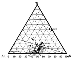
- 1st Embodiment it is a Ti-Al-N type
- 1st Embodiment they are the top view and AA sectional view taken on the line which show a sensor part.
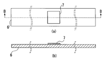
- 1st Embodiment it is a top view and a BB line sectional view showing a thin film thermistor part formation process.
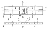
- it is a top view and CC line sectional view showing an electrode formation process.
- 1st Embodiment it is a top view and DD line sectional view showing a protective film formation process.
- 1st Embodiment of the temperature sensor which concerns on this invention it is the top view and front view which show another example. It is the top view and front view which show 2nd Embodiment of the temperature sensor which concerns on this invention.
- 2nd Embodiment of the temperature sensor which concerns on this invention it is the top view and front view which show another example.
- the Example of the temperature sensor which concerns on this invention it is the front view and top view which show the element for film
- Example and comparative example which concern on this invention it is a graph which shows the relationship between 25 degreeC resistivity and B constant.
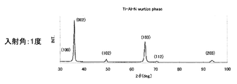
- it is a graph which shows the result of X-ray diffraction (XRD) in case c / axis orientation with Al / (Ti + Al) 0.84 is strong.
- it is a graph which shows the result of X-ray diffraction (XRD) in case a-axis orientation is strong made into Al / (Ti + Al) 0.83.
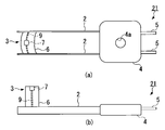
- FIGS. 1 to 7 a first embodiment of a temperature sensor according to the present invention will be described with reference to FIGS. 1 to 7. Note that in some of the drawings used for the following description, the scale is appropriately changed as necessary to make each part recognizable or easily recognizable.
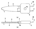
- the temperature sensor 1 of the present embodiment includes a pair of lead frames 2, a sensor unit 3 connected to the pair of lead frames 2, and a lead frame 2 fixed to the pair of lead frames 2. And an insulating holding portion 4 for holding.
- the pair of lead frames 2 are formed of an alloy such as a copper alloy, an iron alloy, or stainless steel, and are supported by a resin holding portion 4 in a state where they are held at a constant interval.
- the pair of lead frames 2 are connected to the pair of lead wires 5 in the holding portion 4.
- the holding portion 4 is formed with an attachment hole 4a.
- the sensor unit 3 includes a strip-shaped insulating film 6, a thin film thermistor unit 7 patterned with a thermistor material at the center of the surface of the insulating film 6, and a thin film thermistor unit 7.
- a pair of comb-shaped electrodes 8 having a plurality of comb portions 8a and patterned so as to face each other, one end of which is connected to the pair of comb-shaped electrodes 8 and the other end of both ends of the insulating film 6
- a pair of pattern electrodes 9 connected to the pair of lead frames 2 and patterned on the surface of the insulating film 6.
- the insulating film 6 has a thin film thermistor portion 7 arranged at the tip end in a state of being bent in a substantially U shape, and both ends are fixed to the pair of lead frames 2.
- the temperature sensor 1 of the present embodiment is a thin film formed on the insulating film 6 except for both ends of the insulating film 6 on which the base end portion (adhesion pad portion 9a) of the pattern electrode 9 is disposed.
- a protective film 10 is provided to cover the thermistor section 7, the comb-shaped electrode 8, and the pattern electrode 9.
- the comb-shaped electrode 8 is formed on the thin film thermistor portion 7.
- the comb-shaped electrode may be formed under the thin film thermistor portion 7.
- the pair of pattern electrodes 9 extends from the comb portion 8 a on the thin film thermistor portion 7 disposed in the central portion of the insulating film 6 to the vicinity of both ends of the insulating film 6. In the vicinity of both ends of the insulating film 6 of the pattern electrode 9, bonding pad portions 9a are formed. Further, the tip ends of the pair of lead frames 2 are connected to the pattern electrode 9 at both ends of the insulating film 6. That is, the lead frame 2 has its tip end bonded to the bonding pad portion 9a of the pattern electrode 9 formed on the insulating film 6 with solder or a conductive resin adhesive.
- the insulating film 6 is fixed to the lead frame 2 with the thin film thermistor portion 7 arranged at the tip end in a state of being bent in a substantially U shape, but in this embodiment, the lead frame 2 It is bent in the state of protruding in the protruding direction.
- the sensor unit 3 is attached to the ends of the pair of lead frames 2 while being bent about the thin film thermistor unit 7 and extending in the protruding direction of the lead frame 2.
- the insulating film 6 is disposed on the inner side surface of the lead frame 2 so that the bonding pad portion 9a and the inner side surface of the lead frame 2 are bonded.
- the insulating film 6 is formed, for example, in a strip shape from a polyimide resin sheet having a thickness of 50 to 125 ⁇ m. In addition, if the thickness of the insulating film 6 is thinner than the above range, it is difficult to obtain sufficient rigidity even if it is bent in a substantially U shape, and if it is thicker than the above range, the responsiveness may be lowered.
- the insulating film 6 can be made of PET: polyethylene terephthalate, PEN: polyethylene naphthalate, or the like, but a polyimide film is desirable for measuring the temperature of the heating roller because the maximum use temperature is as high as 180 ° C.
- the thin film thermistor portion 7 is disposed in the central portion of the insulating film 6 and is formed of a TiAlN thermistor material.
- the pattern electrode 9 and the comb-shaped electrode 8 are formed on the thin film thermistor section 7 with a thickness of 5 to 100 nm of Cr or NiCr, and a noble metal such as Au on the thickness of the bonding layer is 50 to 1000 nm. And an electrode layer formed.
- the pair of comb-shaped electrodes 8 has a comb-shaped pattern in which the comb portions 8a are alternately arranged so as to face each other.
- the comb portion 8 a extends along the extending direction of the insulating film 6. That is, the thin film thermistor portion 7 side, which is the tip portion, is pressed against a rotating heating roller to measure the temperature, but is bent in a U shape with a curvature in the extending direction of the insulating film 6. Therefore, bending stress is also applied to the thin film thermistor portion 7 in the same direction. At this time, since the comb portion 8a extends in the same direction, the thin film thermistor portion 7 is reinforced, and generation of cracks can be suppressed.
- the protective film 10 is an insulating resin film or the like, for example, a polyimide film having a thickness of 20 ⁇ m is adopted.
- the protective film 10 is printed on the insulating film 6 except for the bonding pad portion 9a.
- the protective cover 10 may be formed by bonding a polyimide coverlay film to the insulating film 6 with an adhesive.
- each composition ratio (x, y, z) (atomic%) of the points A, B, C, and D is A (15, 35, 50), B (2.5, 47.5, 50), C (3, 57, 40), D (18, 42, 40).
- the thin film thermistor portion 7 is a columnar crystal that is formed in a film shape with a film thickness of 100 to 1000 nm, for example, and extends in a direction perpendicular to the surface of the film. Further, it is preferable that the c-axis is oriented more strongly than the a-axis in the direction perpendicular to the film surface. Whether the a-axis orientation (100) is strong or the c-axis orientation (002) is strong in the direction perpendicular to the film surface (film thickness direction) is determined using X-ray diffraction (XRD).
- XRD X-ray diffraction
- the manufacturing method of the temperature sensor 1 of the present embodiment includes a thin film thermistor section forming step of patterning the thin film thermistor section 7 on the insulating film 6 and a pair of comb-shaped electrodes 8 facing each other disposed on the thin film thermistor section 7. Then, an electrode forming step of patterning a pair of pattern electrodes 9 on the insulating film 6, a protective film forming step of forming a protective film 10 on the surface of the insulating film 6, and attaching the lead frame 2 to the sensor unit 3 A lead frame attaching step.
- Ti x Al y is used by reactive sputtering in a nitrogen-containing atmosphere using a Ti—Al alloy sputtering target on an insulating film 6 of polyimide film having a thickness of 50 ⁇ m.
- the sputtering conditions at that time were an ultimate vacuum of 5 ⁇ 10 ⁇ 6 Pa, a sputtering gas pressure of 0.4 Pa, a target input power (output) of 200 W, and a nitrogen gas fraction of 20 in a mixed gas atmosphere of Ar gas + nitrogen gas. %.
- a resist solution is applied onto the deposited thermistor film with a bar coater, pre-baked at 110 ° C. for 1 minute 30 seconds, exposed to light with an exposure apparatus, and unnecessary portions are removed with a developer, and further at 150 ° C. Patterning is performed by post-baking for minutes. Thereafter, the thermistor film unnecessary Ti x Al y N z by wet etching in a commercial Ti etchant, as shown in FIG. 4, to a thin film thermistor portion 7 of a desired shape on the resist stripping.
- a 20-nm thick Cr film bonding layer is formed on the thin film thermistor portion 7 and the insulating film 6 by sputtering. Further, an Au film electrode layer is formed to a thickness of 100 nm on the bonding layer by sputtering.
- pre-baking was performed at 110 ° C. for 1 minute 30 seconds, and after exposure with an exposure apparatus, unnecessary portions were removed with a developer, and 150 ° C.
- patterning is performed by post-baking for 5 minutes. Thereafter, unnecessary electrode portions are wet-etched in the order of a commercially available Au etchant and a Cr etchant, and as shown in FIG. 5, desired comb electrodes 8 and pattern electrodes 9 are formed by resist stripping.
- a polyimide varnish is applied thereon by a printing method and cured at 250 ° C. for 30 minutes to form a 20 ⁇ m thick polyimide protective film 10 as shown in FIG.
- the sensor unit 3 is manufactured.
- the tip side of the pair of lead frames 2 is arranged on the bonding pad part 9a of the pattern electrode 9, and as shown in FIG. And the pad portion 9a for bonding are bonded with a conductive resin adhesive. In this way, the temperature sensor 1 is manufactured.
- the insulating film 6 is fixed to the pair of lead frames 2 at both ends thereof with the thin film thermistor portion 7 disposed at the tip portion and bent in a substantially U shape. Therefore, by pressing the bent tip against the object to be measured, the entire insulating film 6 is bent to obtain strong elasticity and rigidity, and the flexibility allows temperature measurement without damaging the object to be measured. Is possible. Moreover, since the deformation
- the insulating film 6 since it is the insulating film 6, heat is hard to escape compared to a metal contact plate, and a high response can be obtained by synergistic effect with the thin film thermistor portion 7 having a small volume. That is, the thin insulating film 6 and the thin film thermistor portion 7 directly formed on the insulating film 6 reduce the overall thickness, and an excellent response can be obtained with a small volume.
- the thin film thermistor portion 7 and the lead frame 2 are connected by the pattern electrodes 9 directly formed on the insulating film 6.
- the effect of the thermal conductivity with the lead frame 2 side is suppressed by the thin wiring with the pattern formed as compared with the case where the lead wires are connected.
- the flatness of the contact part with respect to a measuring object is high, and it contacts a surface, exact temperature detection is possible and it is hard to damage the surface of measuring objects, such as a heating roller to rotate.
- the insulating film 6 is bent in a state of protruding in the protruding direction of the lead frame 2, a measurement object is disposed in front of the protruding direction of the lead frame 2, and the tip of the bent sensor unit 3 is attached. Temperature measurement can be performed by pressing against the measurement object.
- the film is formed by reactive sputtering in a nitrogen-containing atmosphere using a Ti—Al alloy sputtering target, the above-mentioned TiAlN is used.
- the metal nitride material can be formed without firing. Further, by setting the sputtering gas pressure in reactive sputtering to less than 0.67 Pa, a metal nitride material film in which the c-axis is oriented more strongly than the a-axis in the direction perpendicular to the film surface is formed. be able to.
- the thin film thermistor portion 7 is formed of the thermistor material layer on the insulating film 6, the thin film thermistor portion 7 is formed by non-firing and has a high B constant and high heat resistance.
- an insulating film 6 having low heat resistance such as a resin film can be used, and a thin and flexible thermistor sensor having good thermistor characteristics can be obtained.
- substrate materials using ceramics such as alumina are often used in the past. For example, when the thickness is reduced to 0.1 mm, the substrate material is very brittle and easily broken. Therefore, as described above, for example, a very thin film type thermistor sensor (sensor unit 3) having a thickness of 0.1 mm can be obtained.
- the thin film thermistor portion 7 is arranged on the inner side, the sensor portion 3 is bent, and an insulating film is formed on the outer sides of the pair of lead frames 2. Both ends of 6 may be bonded.
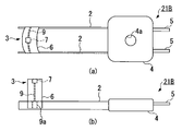
- the difference between the second embodiment and the first embodiment is that, in the first embodiment, the insulating film 6 is bent in a protruding state of the lead frame 2, whereas the second embodiment is different from the second embodiment.
- the temperature sensor 21 is that the insulating film 6 is bent in a state of protruding in a direction orthogonal to the protruding direction of the lead frame 2. That is, in the second embodiment, the insulating film 6 and the pattern electrode 9 extend in a direction orthogonal to the extending direction (protruding direction) of the lead frame 2 in a state where the sensor unit 3 is bent.
- the pair of bonding pad portions 9a formed at both ends of the insulating film 6 and the pair of lead frames 2 are bonded. Note that the lead frame 2 of the second embodiment protrudes longer than the first embodiment.
- the insulating film 6 is bent in a state of protruding in a direction perpendicular to the protruding direction of the lead frame 2. Temperature measurement can be performed by placing a measurement object in front of the orthogonal direction and pressing the bent tip of the sensor unit 3 against the measurement object.
- the insulating film 6 can be installed even when the protruding direction of the insulating film 6 is different from the protruding direction of the lead frame 2 and there is not enough space in the protruding direction of the lead frame 2.
- the thin film thermistor portion 7 is arranged on the inner side, the sensor portion 3 is bent, and an insulating film is formed on the outer sides of the pair of lead frames 2. Both ends of 6 may be bonded.
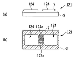
- a film evaluation element 121 shown in FIG. 10 was produced as follows. First, by reactive sputtering, Ti—Al alloy targets having various composition ratios are used to form Si substrates S on a Si wafer with a thermal oxide film at various composition ratios shown in Table 1 having a thickness of 500 nm. A thin film thermistor portion 7 of the formed metal nitride material was formed.
- the sputtering conditions at that time were: ultimate vacuum: 5 ⁇ 10 ⁇ 6 Pa, sputtering gas pressure: 0.1 to 1 Pa, target input power (output): 100 to 500 W, and in a mixed gas atmosphere of Ar gas + nitrogen gas The nitrogen gas fraction was changed to 10 to 100%.
- a 20 nm Cr film was formed on the thin film thermistor portion 7 by sputtering, and a 100 nm Au film was further formed. Furthermore, after applying a resist solution thereon with a spin coater, pre-baking is performed at 110 ° C. for 1 minute 30 seconds, and after exposure with an exposure apparatus, unnecessary portions are removed with a developing solution, and post baking is performed at 150 ° C. for 5 minutes. Patterning. Thereafter, unnecessary electrode portions were wet-etched with a commercially available Au etchant and Cr etchant, and a patterned electrode 124 having a desired comb-shaped electrode portion 124a was formed by resist stripping.
- the X-ray source is MgK ⁇ (350 W)
- the path energy is 58.5 eV
- the measurement interval is 0.125 eV
- the photoelectron extraction angle with respect to the sample surface is 45 deg
- the analysis area is about Quantitative analysis was performed under the condition of 800 ⁇ m ⁇ .
- the quantitative accuracy the quantitative accuracy of N / (Ti + Al + N) is ⁇ 2%
- the quantitative accuracy of Al / (Ti + Al) is ⁇ 1%.
- B constant (K) In (R25 / R50) / (1 / T25-1 / T50)
- T25 (K): 298.15K 25 ° C. is displayed as an absolute temperature
- T50 (K): 323.15K 50 ° C. is displayed as an absolute temperature
- the Ti x Al y N 3 ternary triangular diagram of the composition ratio shown in FIG. 2 of z, the points A, B, C, in a region surrounded by D, ie, "0.70 ⁇ y / (x + y) ⁇ 0.95, 0.4 ⁇ z ⁇ 0.5, x + y + z 1 ”, thermistor characteristics of resistivity: 100 ⁇ cm or more, B constant: 1500 K or more Has been achieved.
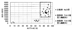
- FIG. 11 shows a graph showing the relationship between the resistivity at 25 ° C. and the B constant based on the above results.
- a high resistance and high B constant region having a specific resistance value at 25 ° C. of 100 ⁇ cm or more and a B constant of 1500 K or more can be realized.
- the B constant varies for the same Al / (Ti + Al) ratio because the amount of nitrogen in the crystal is different.
- Comparative Examples 3 to 12 shown in Table 1 are regions of Al / (Ti + Al) ⁇ 0.7, and the crystal system is cubic NaCl type.
- the NaCl type and the wurtzite type coexist.
- the specific resistance value at 25 ° C. was less than 100 ⁇ cm
- the B constant was less than 1500 K
- the region was low resistance and low B constant.
- Comparative Examples 1 and 2 shown in Table 1 are regions where N / (Ti + Al + N) is less than 40%, and the metal is in a crystalline state with insufficient nitriding.
- Comparative Examples 1 and 2 neither the NaCl type nor the wurtzite type was in a state of very poor crystallinity. Further, in these comparative examples, it was found that both the B constant and the resistance value were very small and close to the metallic behavior.
- Thin film X-ray diffraction (identification of crystal phase)
- the crystal phase of the thin film thermistor portion 7 obtained by the reactive sputtering method was identified by grazing incidence X-ray diffraction.
- the impurity phase is not confirmed, and is a wurtzite type single phase.
- the crystal phase was neither the wurtzite type phase nor the NaCl type phase as described above, and could not be identified in this test. Further, these comparative examples were materials with very poor crystallinity because the peak width of XRD was very wide. This is considered to be a metal phase with insufficient nitriding because it is close to a metallic behavior due to electrical characteristics.
- all the examples of the present invention are films of wurtzite type phase, and since the orientation is strong, is the a-axis orientation strong in the crystal axis in the direction perpendicular to the Si substrate S (film thickness direction)? Whether the c-axis orientation is strong was investigated using XRD. At this time, in order to investigate the orientation of the crystal axis, the peak intensity ratio between (100) (Miller index indicating a-axis orientation) and (002) (Miller index indicating c-axis orientation) was measured.
- the example in which the film was formed at a sputtering gas pressure of less than 0.67 Pa was a film having a (002) strength much stronger than (100) and a stronger c-axis orientation than a-axis orientation.
- the example in which the film was formed at a sputtering gas pressure of 0.67 Pa or higher was a material having a (100) strength much stronger than (002) and a a-axis orientation stronger than the c-axis orientation.
- it formed into a film on the polyimide film on the same film-forming conditions it confirmed that the single phase of the wurtzite type phase was formed similarly.
- orientation does not change.
- FIG. 1 An example of an XRD profile of an example with strong c-axis orientation is shown in FIG.
- Al / (Ti + Al) 0.84 (wurtzite type, hexagonal crystal), and the incident angle was 1 degree.
- the intensity of (002) is much stronger than (100).
- FIG. 1 An example of the XRD profile of an Example with a strong a-axis orientation is shown in FIG.
- Al / (Ti + Al) 0.83 (wurtzite type, hexagonal crystal), and the incident angle was measured as 1 degree.
- the intensity of (100) is much stronger than (002).
- FIG. 1 An example of the XRD profile of the comparative example is shown in FIG.
- Al / (Ti + Al) 0.6 (NaCl type, cubic crystal), and the incident angle was 1 degree.
- a peak that could be indexed as a wurtzite type (space group P6 3 mc (No. 186)) was not detected, and it was confirmed to be a NaCl type single phase.
- the correlation between the crystal structure and the electrical characteristics was further compared in detail for the example of the present invention which is a wurtzite type material.
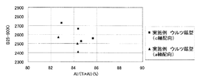
- a material in which the crystal axis having a strong degree of orientation in the direction perpendicular to the substrate surface is the c-axis for the Al / (Ti + Al) ratio is substantially the same (Examples 5, 7, 8, 9) and a material which is a-axis (Examples 19, 20, 21).
- the material having a strong c-axis orientation has a B constant of about 100K higher than that of a material having a strong a-axis orientation.
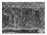
- FIG. 17 shows a cross-sectional SEM photograph of the thin film thermistor portion 7 having a strong c-axis orientation.
- the samples of these examples are those obtained by cleaving the Si substrate S. Moreover, it is the photograph which observed the inclination at an angle of 45 degrees.
- the ionic radius of Ta is much larger than that of Ti or Al, so that a wurtzite type phase cannot be produced in a high concentration Al region. Since the TaAlN system is not a wurtzite type phase, the Ti-Al-N system of the wurtzite type phase is considered to have better heat resistance.
Landscapes
- Engineering & Computer Science (AREA)
- Microelectronics & Electronic Packaging (AREA)
- Physics & Mathematics (AREA)
- General Physics & Mathematics (AREA)
- Electromagnetism (AREA)
- Nonlinear Science (AREA)
- Thermistors And Varistors (AREA)
- Measuring Temperature Or Quantity Of Heat (AREA)
Abstract
Description
なお、上記特許文献1には、感熱素子として ビードサーミスタやチップサーミスタが採用されていると共に、特許文献2には、感熱素子として、アルミナ等の絶縁基板の一面に感熱膜が形成された薄膜サーミスタが採用されている。この薄膜サーミスタは、絶縁基板の一面に形成された感熱膜と、該感熱膜と一対のリードフレームとを接続する一対のリード部と、感熱膜を覆う保護膜とで構成されている。
すなわち、特許文献1に記載の技術では、感熱素子としてビードサーミスタ等を使用しているが、この場合、約1mm程度の球状或いは楕円状であるために、加熱ローラに点接触するために、正確な温度検知が難しい。また、感熱素子に比較的大きな体積があるため、応答性が悪いという不都合があった。さらに、点接触であるために、回転するローラ表面に傷を付けてしまうおそれもあった。
また、特許文献2に記載の技術では、感熱素子として薄膜サーミスタを使用しているので、加熱ローラには面接触することができるが、薄膜サーミスタを構成する絶縁基板やリード部を含めると、やはり体積があるために、応答性が悪いという問題があった。
さらに、特許文献3に記載の技術では、金属の接触板を測定対象物に当てるために測定対象物が傷ついてしまうおそれがあると共に、熱電対及び接触板の体積(厚み等)と、金属の接触板からの熱の逃げとによって応答性が悪いという問題があった。
また、一対のリードフレームが、一対のパターン電極に接続されているので、薄膜サーミスタ部とリードフレームとが絶縁性フィルムに直接形成されたパターン電極で接続されることで、パターン形成された薄い配線により、リード線等で接続された場合に比べてリードフレーム側との熱伝導性の影響が抑制される。なお、測定対象物に対する接触部分の平坦性が高く、面接触するために、正確な温度検知が可能であると共に回転する加熱ローラ等の測定対象物の表面を傷つけ難い。
すなわち、この温度センサでは、絶縁性フィルムが、リードフレームの突出方向に突出した状態で曲げられているので、リードフレームの突出方向前方に測定対象物を配置し、曲げられたセンサ部の先端部を測定対象物に対して押し付けることで温度測定を行うことができる。
すなわち、この温度センサでは、絶縁性フィルムが、リードフレームの突出方向に対して直交する方向に突出した状態で曲げられているので、リードフレームの突出方向に対して直交する方向前方に測定対象物を配置し、曲げられたセンサ部の先端部を測定対象物に対して押し付けることで温度測定を行うことができる。
従来、TiAlNからなる窒化物系サーミスタを形成した温度センサでは、フィルム上にTiAlNからなるサーミスタ材料層と電極とを積層して形成する場合、サーミスタ材料層上にAu等の電極層を成膜し、複数の櫛部を有した櫛型にパターニングしている。しかし、このサーミスタ材料層は、曲率半径が大きく緩やかに曲げられた場合には、クラックが生じ難く抵抗値等の電気特性に変化がないが、曲率半径が小さくきつく曲げた場合に、クラックが発生し易くなり、抵抗値等が大きく変化して電気特性の信頼性が低くなってしまう。特に、フィルムを櫛部の延在方向に直交する方向に小さい曲率半径できつく曲げた場合、櫛部の延在方向に曲げた場合に比べて櫛型電極とサーミスタ材料層との応力差により、電極エッジ付近にクラックが発生し易くなり、電気特性の信頼性が低下してしまう不都合があった。
したがって、本発明は、上記知見から得られたものであり、薄膜サーミスタ部が、一般式:TixAlyNz(0.70≦y/(x+y)≦0.95、0.4≦z≦0.5、x+y+z=1)で示される金属窒化物からなり、その結晶構造が、六方晶系のウルツ鉱型の単相であるので、非焼成で良好なB定数が得られると共に高い耐熱性を有している。
また、上記「y/(x+y)」(すなわち、Al/(Ti+Al))が0.95をこえると、抵抗率が非常に高く、きわめて高い絶縁性を示すため、サーミスタ材料として適用できない。
また、上記「z」(すなわち、N/(Ti+Al+N))が0.4未満であると、金属の窒化量が少ないため、ウルツ鉱型の単相が得られず、十分な高抵抗と高B定数とが得られない。
さらに、上記「z」(すなわち、N/(Ti+Al+N))が0.5を超えると、ウルツ鉱型の単相を得ることができない。このことは、ウルツ鉱型の単相において、窒素サイトにおける欠陥がない場合の化学量論比が、N/(Ti+Al+N)=0.5であることに起因する。
すなわち、本発明に係る温度センサによれば、絶縁性フィルムが、略U字状に曲げられた状態で薄膜サーミスタ部を先端部に配し、両端部が一対のリードフレームに固定されているので、強い弾性及び剛性が得られて測定対象物を傷つけずに温度測定が可能になると共に高い応答性を得ることができる。
また、薄膜サーミスタ部を、一般式:TixAlyNz(0.70≦y/(x+y)≦0.95、0.4≦z≦0.5、x+y+z=1)で示される金属窒化物からなり、その結晶構造が、六方晶系のウルツ鉱型の単相である材料とすることで、非焼成で良好なB定数が得られると共に高い耐熱性が得られる。
したがって、本発明の温度センサによれば、強い弾性と柔軟性とを有したセンサ部による安定した面接触が可能であると共に、高い応答性で正確に温度を測定することができ、複写機やプリンタ等の加熱ローラの温度用として好適である。
上記一対のリードフレーム2は、銅系合金、鉄系合金又はステンレス等の合金で形成されており、樹脂製の保持部4によって互いに一定間隔を保持した状態で支持されている。なお、一対のリードフレーム2は、保持部4内で一対のリード線5に接続されている。また、保持部4には、取付孔4aが形成されている。
上記絶縁性フィルム6は、略U字状に曲げられた状態で薄膜サーミスタ部7を先端部に配し、両端部が一対のリードフレーム2に固定されている。
なお、本実施形態では、薄膜サーミスタ部7の上に櫛型電極8を形成しているが、薄膜サーミスタ部7の下に櫛型電極を形成しても構わない。
さらに、一対のリードフレーム2の先端部が、絶縁性フィルム6の両端部でパターン電極9に接続されている。すなわち、リードフレーム2は、先端側が、絶縁性フィルム6上に形成されたパターン電極9の接着用パッド部9aに、はんだ或いは導電性樹脂接着剤等で接着されている。
一対の櫛型電極8は、互いに対向状態に配されて交互に櫛部8aが並んだ櫛型パターンとされている。
なお、上記点A,B,C,Dの各組成比(x、y、z)(原子%)は、A(15、35、50),B(2.5、47.5、50),C(3、57、40),D(18、42、40)である。
なお、膜の表面に対して垂直方向(膜厚方向)にa軸配向(100)が強いかc軸配向(002)が強いかの判断は、X線回折(XRD)を用いて結晶軸の配向性を調べることで、(100)(a軸配向を示すミラー指数)と(002)(c軸配向を示すミラー指数)とのピーク強度比から、「(100)のピーク強度」/「(002)のピーク強度」が1未満であることで決定する。
本実施形態の温度センサ1の製造方法は、絶縁性フィルム6上に薄膜サーミスタ部7をパターン形成する薄膜サーミスタ部形成工程と、互いに対向した一対の櫛型電極8を薄膜サーミスタ部7上に配して絶縁性フィルム6上に一対のパターン電極9をパターン形成する電極形成工程と、絶縁性フィルム6の表面に保護膜10を形成する保護膜形成工程と、センサ部3にリードフレーム2を取り付けるリードフレーム取り付け工程とを有している。
次に、成膜した電極層の上にレジスト液をバーコーターで塗布した後、110℃で1分30秒のプリベークを行い、露光装置で感光後、現像液で不要部分を除去し、150℃で5分のポストベークにてパターニングを行う。その後、不要な電極部分を市販のAuエッチャント及びCrエッチャントの順番でウェットエッチングを行い、図5に示すように、レジスト剥離にて所望の櫛型電極8及びパターン電極9を形成する。
次に、センサ部3を折り曲げた状態で、一対のリードフレーム2の先端側をパターン電極9の接着用パッド部9a上に配して、図1に示すように、リードフレーム2の先端内面側と接着用パッド部9aとを導電性樹脂接着剤により接着する。このようにして、温度センサ1が作製される。
また、この金属窒化物材料では、膜の表面に対して垂直方向に延在している柱状結晶であるので、膜の結晶性が高く、高い耐熱性が得られる。
さらに、この金属窒化物材料では、膜の表面に対して垂直方向にa軸よりc軸を強く配向させることで、a軸配向が強い場合に比べて高いB定数が得られる。
また、反応性スパッタにおけるスパッタガス圧を、0.67Pa未満に設定することで、膜の表面に対して垂直方向にa軸よりc軸が強く配向している金属窒化物材料の膜を形成することができる。
また、従来アルミナ等のセラミックスを用いた基板材料がしばしば用いられ、例えば、厚さ0.1mmへと薄くすると非常に脆く壊れやすい等の問題があったが、本発明においてはフィルムを用いることができるので、上記のように、例えば厚さ0.1mmの非常に薄いフィルム型サーミスタセンサ(センサ部3)を得ることができる。
すなわち、第2実施形態では、センサ部3が折り曲げられた状態で、リードフレーム2の延在方向(突出方向)に対して直交する方向に絶縁性フィルム6及びパターン電極9が延在するように、絶縁性フィルム6の両端部に形成された一対の接着用パッド部9aと一対のリードフレーム2とが接着されている。なお、第2実施形態のリードフレーム2は、第1実施形態よりも長く突出している。
なお、第2実施形態の他の例として、図9に示す温度センサ21Bのように、薄膜サーミスタ部7を内側に配してセンサ部3を折り曲げ、一対のリードフレーム2の外側に絶縁性フィルム6の両端部を接着しても構わない。
本発明のサーミスタ材料層(薄膜サーミスタ部7)の評価を行う実施例及び比較例として、図10に示す膜評価用素子121を次のように作製した。
まず、反応性スパッタ法にて、様々な組成比のTi−Al合金ターゲットを用いて、Si基板Sとなる熱酸化膜付きSiウエハ上に、厚さ500nmの表1に示す様々な組成比で形成された金属窒化物材料の薄膜サーミスタ部7を形成した。その時のスパッタ条件は、到達真空度:5×10⁻⁶Pa、スパッタガス圧:0.1~1Pa、ターゲット投入電力(出力):100~500Wで、Arガス+窒素ガスの混合ガス雰囲気下において、窒素ガス分率を10~100%と変えて作製した。
なお、比較としてTixAlyNzの組成比が本発明の範囲外であって結晶系が異なる比較例についても同様に作製して評価を行った。
(1)組成分析
反応性スパッタ法にて得られた薄膜サーミスタ部7について、X線光電子分光法(XPS)にて元素分析を行った。このXPSでは、Arスパッタにより、最表面から深さ20nmのスパッタ面において、定量分析を実施した。その結果を表1に示す。なお、以下の表中の組成比は「原子%」で示している。
反応性スパッタ法にて得られた薄膜サーミスタ部7について、4端子法にて25℃での比抵抗を測定した。その結果を表1に示す。
(3)B定数測定
膜評価用素子121の25℃及び50℃の抵抗値を恒温槽内で測定し、25℃と50℃との抵抗値よりB定数を算出した。その結果を表1に示す。
B定数(K)=In(R25/R50)/(1/T25−1/T50)
R25(Ω):25℃における抵抗値
R50(Ω):50℃における抵抗値
T25(K):298.15K 25℃を絶対温度表示
T50(K):323.15K 50℃を絶対温度表示
反応性スパッタ法にて得られた薄膜サーミスタ部7を、視斜角入射X線回折(Grazing Incidence X−ray Diffraction)により、結晶相を同定した。この薄膜X線回折は、微小角X線回折実験であり、管球をCuとし、入射角を1度とすると共に2θ=20~130度の範囲で測定した。
なお、表1に示す比較例1,2は、上述したように結晶相がウルツ鉱型相でもNaCl型相でもなく、本試験においては同定できなかった。また、これらの比較例は、XRDのピーク幅が非常に広いことから、非常に結晶性の劣る材料であった。これは、電気特性により金属的振舞いに近いことから、窒化不足の金属相になっていると考えられる。

なお、同じ成膜条件でポリイミドフィルムに成膜しても、同様にウルツ鉱型相の単一相が形成されていることを確認している。また、同じ成膜条件でポリイミドフィルムに成膜しても、配向性は変わらないことを確認している。
また、a軸配向が強い実施例のXRDプロファイルの一例を、図14に示す。この実施例は、Al/(Ti+Al)=0.83(ウルツ鉱型、六方晶)であり、入射角を1度として測定した。この結果からわかるように、この実施例では、(002)よりも(100)の強度が非常に強くなっている。
表2及び図16に示すように、Al/(Ti+Al)比がほぼ同じ比率のものに対し、基板面に垂直方向の配向度の強い結晶軸がc軸である材料(実施例5,7,8,9)とa軸である材料(実施例19,20,21)とがある。

次に、薄膜サーミスタ部7の断面における結晶形態を示す一例として、熱酸化膜付きSi基板S上に成膜された実施例(Al/(Ti+Al)=0.84,ウルツ鉱型、六方晶、c軸配向性が強い)の薄膜サーミスタ部7における断面SEM写真を、図17に示す。また、別の実施例(Al/(Ti+Al)=0.83,ウルツ鉱型六方晶、a軸配向性が強い)の薄膜サーミスタ部7における断面SEM写真を、図18に示す。
これら実施例のサンプルは、Si基板Sをへき開破断したものを用いている。また、45°の角度で傾斜観察した写真である。
表1に示す実施例及び比較例において、大気中,125℃,1000hの耐熱試験前後における抵抗値及びB定数を評価した。その結果を表3に示す。なお、比較として従来のTa−Al−N系材料による比較例も同様に評価した。
これらの結果からわかるように、Al濃度及び窒素濃度は異なるものの、Ta−Al−N系である比較例と同じB定数で比較したとき、耐熱試験前後における電気特性変化でみたときの耐熱性は、Ti−Al−N系のほうが優れている。なお、実施例5,8はc軸配向が強い材料であり、実施例21,24はa軸配向が強い材料である。両者を比較すると、c軸配向が強い実施例の方がa軸配向が強い実施例に比べて僅かに耐熱性が向上している。

Claims (4)
- 一対のリードフレームと、
前記一対のリードフレームに接続されたセンサ部と、
前記一対のリードフレームに固定されて前記リードフレームを保持する絶縁性の保持部とを備え、
前記センサ部が、帯状の絶縁性フィルムと、該絶縁性フィルムの表面の中央部にサーミスタ材料でパターン形成された薄膜サーミスタ部と、前記薄膜サーミスタ部の上及び下の少なくとも一方に複数の櫛部を有して互いに対向してパターン形成された一対の櫛型電極と、一端が前記一対の櫛型電極に接続されていると共に他端が前記絶縁性フィルムの両端部で前記一対のリードフレームに接続され前記絶縁性フィルムの表面にパターン形成された一対のパターン電極とを備え、
前記絶縁性フィルムが、略U字状に曲げられた状態で前記薄膜サーミスタ部を先端部に配し、両端部が前記一対のリードフレームに固定されていることを特徴とする温度センサ。 - 請求項1に記載の温度センサにおいて、
前記絶縁性フィルムが、前記リードフレームの突出方向に突出した状態で曲げられていることを特徴とする温度センサ。 - 請求項1に記載の温度センサにおいて、
前記絶縁性フィルムが、前記リードフレームの突出方向に対して直交する方向に突出した状態で曲げられていることを特徴とする温度センサ。 - 請求項1に記載の温度センサにおいて、
前記薄膜サーミスタ部が、一般式:TixAlyNz(0.70≦y/(x+y)≦0.95、0.4≦z≦0.5、x+y+z=1)で示される金属窒化物からなり、その結晶構造が、六方晶系のウルツ鉱型の単相であることを特徴とする温度センサ。
Priority Applications (4)
| Application Number | Priority Date | Filing Date | Title |
|---|---|---|---|
| CN201380062949.8A CN104823031B (zh) | 2013-01-31 | 2013-12-17 | 温度传感器 |
| EP13873239.1A EP2952863B1 (en) | 2013-01-31 | 2013-12-17 | Temperature sensor |
| US14/763,477 US9448123B2 (en) | 2013-01-31 | 2013-12-17 | Temperature sensor |
| KR1020157020561A KR101972201B1 (ko) | 2013-01-31 | 2013-12-17 | 온도 센서 |
Applications Claiming Priority (2)
| Application Number | Priority Date | Filing Date | Title |
|---|---|---|---|
| JP2013016307A JP5928829B2 (ja) | 2013-01-31 | 2013-01-31 | 温度センサ |
| JP2013-016307 | 2013-01-31 |
Publications (1)
| Publication Number | Publication Date |
|---|---|
| WO2014119206A1 true WO2014119206A1 (ja) | 2014-08-07 |
Family
ID=51261930
Family Applications (1)
| Application Number | Title | Priority Date | Filing Date |
|---|---|---|---|
| PCT/JP2013/084768 Ceased WO2014119206A1 (ja) | 2013-01-31 | 2013-12-17 | 温度センサ |
Country Status (7)
| Country | Link |
|---|---|
| US (1) | US9448123B2 (ja) |
| EP (1) | EP2952863B1 (ja) |
| JP (1) | JP5928829B2 (ja) |
| KR (1) | KR101972201B1 (ja) |
| CN (1) | CN104823031B (ja) |
| TW (1) | TWI588459B (ja) |
| WO (1) | WO2014119206A1 (ja) |
Families Citing this family (12)
| Publication number | Priority date | Publication date | Assignee | Title |
|---|---|---|---|---|
| JP5896160B2 (ja) * | 2012-09-28 | 2016-03-30 | 三菱マテリアル株式会社 | 温度センサ |
| JP6052609B2 (ja) * | 2013-01-31 | 2016-12-27 | 三菱マテリアル株式会社 | 温度センサ |
| JP5928831B2 (ja) * | 2013-03-21 | 2016-06-01 | 三菱マテリアル株式会社 | 温度センサ |
| JP6515569B2 (ja) * | 2015-02-17 | 2019-05-22 | 三菱マテリアル株式会社 | 温度センサ |
| JP2017134024A (ja) * | 2016-01-29 | 2017-08-03 | 三菱マテリアル株式会社 | 温度センサ |
| CN106197725A (zh) * | 2016-07-07 | 2016-12-07 | 安徽晶格尔电子有限公司 | 一种单面极热电阻温度传感器 |
| WO2018043346A1 (ja) * | 2016-09-01 | 2018-03-08 | パナソニックIpマネジメント株式会社 | 機能性素子及び温度センサ |
| JP2018146403A (ja) * | 2017-03-06 | 2018-09-20 | Koa株式会社 | 温度センサ素子 |
| CN108007595B (zh) * | 2017-11-21 | 2020-01-14 | 西北工业大学 | 一种探头式薄膜热电偶温度传感器及其制作方法 |
| JP6791225B2 (ja) * | 2018-10-15 | 2020-11-25 | 三菱マテリアル株式会社 | 温度センサ |
| JP2021056161A (ja) * | 2019-10-01 | 2021-04-08 | 日東電工株式会社 | 導電フィルムおよびその製造方法、ならびに温度センサフィルムおよびその製造方法 |
| CN113970576B (zh) * | 2021-09-14 | 2022-05-06 | 中国电器科学研究院股份有限公司 | 一种表面盐沉降量的实时监测装置及方法 |
Citations (8)
| Publication number | Priority date | Publication date | Assignee | Title |
|---|---|---|---|---|
| JPS5682629U (ja) * | 1979-11-30 | 1981-07-03 | ||
| JPH0629793B2 (ja) | 1987-02-20 | 1994-04-20 | 石塚電子株式会社 | 温度センサ |
| JPH07198504A (ja) | 1993-12-30 | 1995-08-01 | Anritsu Keiki Kk | 接触式表面温度センサ |
| JP2000074752A (ja) | 1998-09-01 | 2000-03-14 | Ishizuka Electronics Corp | 温度センサ |
| JP2004319737A (ja) | 2003-04-16 | 2004-11-11 | Osaka Prefecture | サーミスタ用材料及びその製造方法 |
| JP2008058226A (ja) * | 2006-09-01 | 2008-03-13 | Canon Inc | 温度検知装置及び加熱装置 |
| JP2012068116A (ja) * | 2010-09-23 | 2012-04-05 | Mitsubishi Materials Corp | 温度センサ付き電池 |
| JP2012182258A (ja) * | 2011-02-28 | 2012-09-20 | Mitsubishi Materials Corp | 温度センサ付き非接触給電装置 |
Family Cites Families (9)
| Publication number | Priority date | Publication date | Assignee | Title |
|---|---|---|---|---|
| GB2140615B (en) * | 1983-03-22 | 1987-03-18 | Standard Telephones Cables Ltd | Thermistor composite |
| DE4206082C1 (ja) | 1992-02-27 | 1993-04-08 | Siemens Ag, 8000 Muenchen, De | |
| JP3756607B2 (ja) * | 1997-02-27 | 2006-03-15 | 石塚電子株式会社 | 温度センサ |
| JP3815362B2 (ja) * | 2002-04-08 | 2006-08-30 | 株式会社村田製作所 | 温度検出素子およびこれを備える回路基板 |
| JP2011044621A (ja) * | 2009-08-23 | 2011-03-03 | Mitsubishi Materials Corp | 温度センサ |
| JP5316959B2 (ja) * | 2010-03-17 | 2013-10-16 | 三菱マテリアル株式会社 | 薄膜サーミスタセンサ |
| JP5652082B2 (ja) * | 2010-09-23 | 2015-01-14 | 三菱マテリアル株式会社 | 温度センサ付き電解コンデンサ |
| JP5560468B2 (ja) * | 2011-01-29 | 2014-07-30 | 三菱マテリアル株式会社 | 薄膜サーミスタセンサおよびその製造方法 |
| CN202485824U (zh) * | 2012-04-27 | 2012-10-10 | 肇庆市金龙宝电子有限公司 | 一种旁夹式特种外形ntc热敏电阻温度传感器 |
-
2013
- 2013-01-31 JP JP2013016307A patent/JP5928829B2/ja not_active Expired - Fee Related
- 2013-12-17 KR KR1020157020561A patent/KR101972201B1/ko not_active Expired - Fee Related
- 2013-12-17 CN CN201380062949.8A patent/CN104823031B/zh not_active Expired - Fee Related
- 2013-12-17 US US14/763,477 patent/US9448123B2/en not_active Expired - Fee Related
- 2013-12-17 WO PCT/JP2013/084768 patent/WO2014119206A1/ja not_active Ceased
- 2013-12-17 EP EP13873239.1A patent/EP2952863B1/en not_active Not-in-force
- 2013-12-23 TW TW102147771A patent/TWI588459B/zh not_active IP Right Cessation
Patent Citations (8)
| Publication number | Priority date | Publication date | Assignee | Title |
|---|---|---|---|---|
| JPS5682629U (ja) * | 1979-11-30 | 1981-07-03 | ||
| JPH0629793B2 (ja) | 1987-02-20 | 1994-04-20 | 石塚電子株式会社 | 温度センサ |
| JPH07198504A (ja) | 1993-12-30 | 1995-08-01 | Anritsu Keiki Kk | 接触式表面温度センサ |
| JP2000074752A (ja) | 1998-09-01 | 2000-03-14 | Ishizuka Electronics Corp | 温度センサ |
| JP2004319737A (ja) | 2003-04-16 | 2004-11-11 | Osaka Prefecture | サーミスタ用材料及びその製造方法 |
| JP2008058226A (ja) * | 2006-09-01 | 2008-03-13 | Canon Inc | 温度検知装置及び加熱装置 |
| JP2012068116A (ja) * | 2010-09-23 | 2012-04-05 | Mitsubishi Materials Corp | 温度センサ付き電池 |
| JP2012182258A (ja) * | 2011-02-28 | 2012-09-20 | Mitsubishi Materials Corp | 温度センサ付き非接触給電装置 |
Non-Patent Citations (1)
| Title |
|---|
| See also references of EP2952863A4 |
Also Published As
| Publication number | Publication date |
|---|---|
| KR101972201B1 (ko) | 2019-04-24 |
| KR20150111934A (ko) | 2015-10-06 |
| TWI588459B (zh) | 2017-06-21 |
| JP2014149153A (ja) | 2014-08-21 |
| EP2952863A4 (en) | 2016-12-28 |
| JP5928829B2 (ja) | 2016-06-01 |
| US20150362381A1 (en) | 2015-12-17 |
| EP2952863B1 (en) | 2017-09-13 |
| US9448123B2 (en) | 2016-09-20 |
| CN104823031A (zh) | 2015-08-05 |
| TW201443410A (zh) | 2014-11-16 |
| CN104823031B (zh) | 2017-04-05 |
| EP2952863A1 (en) | 2015-12-09 |
Similar Documents
| Publication | Publication Date | Title |
|---|---|---|
| JP5928829B2 (ja) | 温度センサ | |
| JP5896157B2 (ja) | 温度センサ | |
| JP5896160B2 (ja) | 温度センサ | |
| JP5776942B2 (ja) | 温度センサ | |
| JP5939396B2 (ja) | 温度センサ | |
| JP5928831B2 (ja) | 温度センサ | |
| JP6108156B2 (ja) | 温度センサ | |
| JP2013211434A (ja) | サーミスタ用金属窒化物膜及びその製造方法並びにフィルム型サーミスタセンサ | |
| JP6052614B2 (ja) | 温度センサ | |
| JP6128379B2 (ja) | 非接触温度センサ | |
| JP6052609B2 (ja) | 温度センサ | |
| JP6011286B2 (ja) | 温度センサ | |
| JP6011285B2 (ja) | 温度センサ | |
| JP6015517B2 (ja) | 温度センサ | |
| JP2014169874A (ja) | 温度センサ | |
| JP5796719B2 (ja) | 温度センサ及びその製造方法 | |
| JP2014109504A (ja) | 温度センサ | |
| JP5939397B2 (ja) | 温度センサ |
Legal Events
| Date | Code | Title | Description |
|---|---|---|---|
| 121 | Ep: the epo has been informed by wipo that ep was designated in this application |
Ref document number: 13873239 Country of ref document: EP Kind code of ref document: A1 |
|
| WWE | Wipo information: entry into national phase |
Ref document number: 14763477 Country of ref document: US |
|
| ENP | Entry into the national phase |
Ref document number: 20157020561 Country of ref document: KR Kind code of ref document: A |
|
| REEP | Request for entry into the european phase |
Ref document number: 2013873239 Country of ref document: EP |
|
| WWE | Wipo information: entry into national phase |
Ref document number: 2013873239 Country of ref document: EP |
|
| NENP | Non-entry into the national phase |
Ref country code: DE |