WO2014119476A1 - 押圧センサ付き表示パネル、および押圧入力機能付き電子機器 - Google Patents
押圧センサ付き表示パネル、および押圧入力機能付き電子機器 Download PDFInfo
- Publication number
- WO2014119476A1 WO2014119476A1 PCT/JP2014/051457 JP2014051457W WO2014119476A1 WO 2014119476 A1 WO2014119476 A1 WO 2014119476A1 JP 2014051457 W JP2014051457 W JP 2014051457W WO 2014119476 A1 WO2014119476 A1 WO 2014119476A1
- Authority
- WO
- WIPO (PCT)
- Prior art keywords
- display panel
- pressure sensor
- piezoelectric
- sensor
- piezoelectric film
- Prior art date
- Legal status (The legal status is an assumption and is not a legal conclusion. Google has not performed a legal analysis and makes no representation as to the accuracy of the status listed.)
- Ceased
Links
Images




Classifications
-
- G—PHYSICS
- G02—OPTICS
- G02F—OPTICAL DEVICES OR ARRANGEMENTS FOR THE CONTROL OF LIGHT BY MODIFICATION OF THE OPTICAL PROPERTIES OF THE MEDIA OF THE ELEMENTS INVOLVED THEREIN; NON-LINEAR OPTICS; FREQUENCY-CHANGING OF LIGHT; OPTICAL LOGIC ELEMENTS; OPTICAL ANALOGUE/DIGITAL CONVERTERS
- G02F1/00—Devices or arrangements for the control of the intensity, colour, phase, polarisation or direction of light arriving from an independent light source, e.g. switching, gating or modulating; Non-linear optics
- G02F1/01—Devices or arrangements for the control of the intensity, colour, phase, polarisation or direction of light arriving from an independent light source, e.g. switching, gating or modulating; Non-linear optics for the control of the intensity, phase, polarisation or colour
- G02F1/13—Devices or arrangements for the control of the intensity, colour, phase, polarisation or direction of light arriving from an independent light source, e.g. switching, gating or modulating; Non-linear optics for the control of the intensity, phase, polarisation or colour based on liquid crystals, e.g. single liquid crystal display cells
- G02F1/133—Constructional arrangements; Operation of liquid crystal cells; Circuit arrangements
- G02F1/1333—Constructional arrangements; Manufacturing methods
- G02F1/13338—Input devices, e.g. touch panels
-
- G—PHYSICS
- G02—OPTICS
- G02F—OPTICAL DEVICES OR ARRANGEMENTS FOR THE CONTROL OF LIGHT BY MODIFICATION OF THE OPTICAL PROPERTIES OF THE MEDIA OF THE ELEMENTS INVOLVED THEREIN; NON-LINEAR OPTICS; FREQUENCY-CHANGING OF LIGHT; OPTICAL LOGIC ELEMENTS; OPTICAL ANALOGUE/DIGITAL CONVERTERS
- G02F1/00—Devices or arrangements for the control of the intensity, colour, phase, polarisation or direction of light arriving from an independent light source, e.g. switching, gating or modulating; Non-linear optics
- G02F1/01—Devices or arrangements for the control of the intensity, colour, phase, polarisation or direction of light arriving from an independent light source, e.g. switching, gating or modulating; Non-linear optics for the control of the intensity, phase, polarisation or colour
- G02F1/13—Devices or arrangements for the control of the intensity, colour, phase, polarisation or direction of light arriving from an independent light source, e.g. switching, gating or modulating; Non-linear optics for the control of the intensity, phase, polarisation or colour based on liquid crystals, e.g. single liquid crystal display cells
- G02F1/133—Constructional arrangements; Operation of liquid crystal cells; Circuit arrangements
- G02F1/1333—Constructional arrangements; Manufacturing methods
- G02F1/1335—Structural association of cells with optical devices, e.g. polarisers or reflectors
- G02F1/133528—Polarisers
-
- G—PHYSICS
- G02—OPTICS
- G02F—OPTICAL DEVICES OR ARRANGEMENTS FOR THE CONTROL OF LIGHT BY MODIFICATION OF THE OPTICAL PROPERTIES OF THE MEDIA OF THE ELEMENTS INVOLVED THEREIN; NON-LINEAR OPTICS; FREQUENCY-CHANGING OF LIGHT; OPTICAL LOGIC ELEMENTS; OPTICAL ANALOGUE/DIGITAL CONVERTERS
- G02F1/00—Devices or arrangements for the control of the intensity, colour, phase, polarisation or direction of light arriving from an independent light source, e.g. switching, gating or modulating; Non-linear optics
- G02F1/01—Devices or arrangements for the control of the intensity, colour, phase, polarisation or direction of light arriving from an independent light source, e.g. switching, gating or modulating; Non-linear optics for the control of the intensity, phase, polarisation or colour
- G02F1/13—Devices or arrangements for the control of the intensity, colour, phase, polarisation or direction of light arriving from an independent light source, e.g. switching, gating or modulating; Non-linear optics for the control of the intensity, phase, polarisation or colour based on liquid crystals, e.g. single liquid crystal display cells
- G02F1/133—Constructional arrangements; Operation of liquid crystal cells; Circuit arrangements
- G02F1/1333—Constructional arrangements; Manufacturing methods
- G02F1/1335—Structural association of cells with optical devices, e.g. polarisers or reflectors
- G02F1/13363—Birefringent elements, e.g. for optical compensation
-
- G—PHYSICS
- G06—COMPUTING OR CALCULATING; COUNTING
- G06F—ELECTRIC DIGITAL DATA PROCESSING
- G06F3/00—Input arrangements for transferring data to be processed into a form capable of being handled by the computer; Output arrangements for transferring data from processing unit to output unit, e.g. interface arrangements
- G06F3/01—Input arrangements or combined input and output arrangements for interaction between user and computer
- G06F3/03—Arrangements for converting the position or the displacement of a member into a coded form
- G06F3/041—Digitisers, e.g. for touch screens or touch pads, characterised by the transducing means
- G06F3/0414—Digitisers, e.g. for touch screens or touch pads, characterised by the transducing means using force sensing means to determine a position
-
- G—PHYSICS
- G06—COMPUTING OR CALCULATING; COUNTING
- G06F—ELECTRIC DIGITAL DATA PROCESSING
- G06F3/00—Input arrangements for transferring data to be processed into a form capable of being handled by the computer; Output arrangements for transferring data from processing unit to output unit, e.g. interface arrangements
- G06F3/01—Input arrangements or combined input and output arrangements for interaction between user and computer
- G06F3/03—Arrangements for converting the position or the displacement of a member into a coded form
- G06F3/041—Digitisers, e.g. for touch screens or touch pads, characterised by the transducing means
- G06F3/0414—Digitisers, e.g. for touch screens or touch pads, characterised by the transducing means using force sensing means to determine a position
- G06F3/04144—Digitisers, e.g. for touch screens or touch pads, characterised by the transducing means using force sensing means to determine a position using an array of force sensing means
-
- G—PHYSICS
- G06—COMPUTING OR CALCULATING; COUNTING
- G06F—ELECTRIC DIGITAL DATA PROCESSING
- G06F3/00—Input arrangements for transferring data to be processed into a form capable of being handled by the computer; Output arrangements for transferring data from processing unit to output unit, e.g. interface arrangements
- G06F3/01—Input arrangements or combined input and output arrangements for interaction between user and computer
- G06F3/03—Arrangements for converting the position or the displacement of a member into a coded form
- G06F3/041—Digitisers, e.g. for touch screens or touch pads, characterised by the transducing means
- G06F3/047—Digitisers, e.g. for touch screens or touch pads, characterised by the transducing means using sets of wires, e.g. crossed wires
-
- G—PHYSICS
- G09—EDUCATION; CRYPTOGRAPHY; DISPLAY; ADVERTISING; SEALS
- G09F—DISPLAYING; ADVERTISING; SIGNS; LABELS OR NAME-PLATES; SEALS
- G09F9/00—Indicating arrangements for variable information in which the information is built-up on a support by selection or combination of individual elements
- G09F9/30—Indicating arrangements for variable information in which the information is built-up on a support by selection or combination of individual elements in which the desired character or characters are formed by combining individual elements
- G09F9/35—Indicating arrangements for variable information in which the information is built-up on a support by selection or combination of individual elements in which the desired character or characters are formed by combining individual elements being liquid crystals
-
- G—PHYSICS
- G02—OPTICS
- G02B—OPTICAL ELEMENTS, SYSTEMS OR APPARATUS
- G02B5/00—Optical elements other than lenses
- G02B5/30—Polarising elements
-
- G—PHYSICS
- G02—OPTICS
- G02B—OPTICAL ELEMENTS, SYSTEMS OR APPARATUS
- G02B5/00—Optical elements other than lenses
- G02B5/30—Polarising elements
- G02B5/3083—Birefringent or phase retarding elements
Definitions
- the present invention relates to a display panel with a press sensor capable of inputting a pressing operation by operating a display screen with a finger or the like, and an electronic device with a press input function including the display panel with the press sensor.
- Patent Document 1 a touch sensor that detects an operation position is arranged on the surface side of a display panel. When the operator touches the operation surface, the touch sensor detects the touch position. The electronic device executes processing according to the operation position.
- each component constituting the electronic device is arranged in the following positional relationship.
- a surface polarizing plate is disposed on the operation surface (outermost surface).
- a touch panel is disposed on the surface opposite to the operation surface of the surface polarizing plate.
- a liquid crystal panel made of a pair of glasses sandwiched with liquid crystal is disposed on the side of the touch panel opposite to the surface polarizing plate.
- a back surface side polarizing plate is disposed on the surface of the liquid crystal panel opposite to the touch panel. That is, a touch panel is arrange
- the liquid crystal display when the liquid crystal display is a transmissive type, light from the backlight disposed further on the back side of the back side polarizing plate is transmitted in the order of the back side polarizing plate, the liquid crystal panel, the touch sensor, and the front polarizing plate. And exits to the operation surface.
- a polarizing plate on the back side is not necessary, and instead, for example, a reflecting plate is installed.
- light incident from the operation surface is reflected on the surface polarizing plate, touch sensor, liquid crystal panel, reflecting plate, , The touch sensor, and the surface polarizing plate are transmitted in this order to return to the operation surface.
- the front polarizing plate and the rear polarizing plate utilize the property of transmitting only waves (light waves) that vibrate in a specific direction, and in combination with a liquid crystal panel, the contrast and transmissivity are set to predetermined values and the appearance is improved. I am letting.
- a pressing sensor is constructed from a chiral polymer piezoelectric element so that the amount of pressing can be detected.
- chiral polymer piezoelectric elements have birefringence.
- the refractive index of a wave oscillating in a direction parallel to the stretching direction of uniaxially stretched L-type polylactic acid (PLLA) is 1.47.
- the refractive index of a wave oscillating in a direction perpendicular to the stretching direction of uniaxially stretched L-type polylactic acid (PLLA) is 1.45. That is, it has the property of retardation.
- a pressure sensor having such birefringence When a pressure sensor having such birefringence is incorporated in the above-mentioned thin display panel, if it is a transmissive type, it is disposed between the front polarizing plate and the rear polarizing plate, and if it is a reflective type, it is in the light guide direction. It has been found that when it is disposed between the surface polarizing plates twice along the line, the target color changes, and a desired image color cannot be obtained.
- an object of the present invention is to provide a display panel with a pressure sensor that can reproduce a desired color in a display panel in which the amount of pressing can be detected by a piezoelectric element of a chiral polymer.
- the display panel with a pressure sensor of the present invention is characterized by having the following configuration.
- the display panel with a pressure sensor includes a display panel, a pressure sensor, and a phase compensation film.
- the display panel includes an image forming panel that forms a display image by controlling light emitted to the front surface side, and a surface polarizing plate disposed on the front surface side of the image forming panel.
- the pressure sensor has a piezoelectric film formed of a chiral polymer.
- the birefringence of the piezoelectric film is compensated by the birefringence of the phase compensation film and offset.
- the light emitted from the image forming panel is displayed without causing a phase difference depending on the direction.
- both the pressure sensor and the phase compensation film are disposed between the image forming panel and the surface polarizing plate.
- the birefringence of the piezoelectric film is compensated and offset by the birefringence of the phase compensation film, so that the light emitted from the image forming panel is phase-dependent.
- the surface polarizing plate is reached without any difference.
- the chiral polymer forming the piezoelectric film is polylactic acid, and the polylactic acid is preferably stretched at least in a uniaxial direction.
- This configuration shows a preferred mode of the piezoelectric film.
- polylactic acid By using polylactic acid, it is possible to realize a display panel with a pressure sensor having excellent translucency and high pressure detection sensitivity.
- the phase compensation film has a phase difference opposite to that of the piezoelectric film of the pressure sensor.
- the birefringence of the piezoelectric film is more effectively offset by the phase compensation film, and the phase difference depending on the direction can be further suppressed.
- the phase compensation film is polylactic acid stretched at least in a uniaxial direction, and the uniaxial stretch direction of the piezoelectric film and the uniaxial stretch direction of the phase compensation film are orthogonal to each other. Preferably it is.
- This configuration shows a preferred aspect of the phase compensation film.
- the phase compensation film may have a position detection sensor function for detecting a touch position.
- position detection can be performed together with pressure detection.
- the pressure sensor has a position detection sensor function for detecting a touch position.
- the press sensor and the position detection sensor are integrally formed.
- the display panel with a press sensor which has an operation position detection function can be formed thinly.
- An electronic device with a press input function includes a display panel with a press sensor according to any one of the above, a calculation unit that detects a pressing amount from a detection signal of the press sensor, a display surface side that is open, and a display panel with a press sensor. And a housing in which the unit is housed.
- a desired color can be reproduced even in a display panel including a pressure sensor having birefringence.
- 1 is an external perspective view of an electronic device with a press input function according to a first embodiment of the present invention. It is sectional drawing of the electronic device with a press input function which concerns on the 1st Embodiment of this invention. It is the top view which decomposed
- FIG. 1 is an external perspective view of an electronic apparatus with a press input function according to a first embodiment of the present invention.
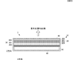
- FIG. 2 is a cross-sectional view of the electronic device with a press input function according to the first embodiment of the present invention.
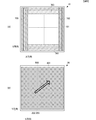
- FIG. 3 is an exploded plan view of the pressure sensor according to the first embodiment of the present invention.
- the electronic device 1 with a press input function includes a housing 50 having a substantially rectangular parallelepiped shape.
- the surface side of the housing 50 is open.
- the width direction (lateral direction) of the housing 50 is the X direction
- the length direction (vertical direction) is the Y direction
- the thickness direction is the Z direction.
- a case where the length of the housing 50 in the X direction is shorter than the length of the housing 50 in the Y direction is shown.
- the length in the X direction may be longer than the length in the Y direction.
- a display panel 10 with a pressure sensor, a protective member 40, and an arithmetic circuit module 60 are arranged in the housing 50. These are arranged in the order of the protective member 40, the display panel with pressure sensor 10, and the arithmetic circuit module 60 along the Z direction in order from the opening surface (display surface) side of the housing 50.
- the display panel with a pressure sensor 10 includes a pressure sensor 20 and a display panel 30.
- the press sensor 20 includes a flat film-like piezoelectric film 201 and electrodes 202 and 203. Electrodes 202 and 203 are arranged on both flat plate surfaces (main surfaces) of the piezoelectric film 201. The electrodes 202 and 203 are formed on substantially the entire flat plate surface of the piezoelectric film 201.
- the piezoelectric film 204 is disposed on the surface of the electrode 203 opposite to the piezoelectric film 201.
- Piezoelectric films 201 and 204 are films formed from a chiral polymer.
- polylactic acid (PLA) particularly L-type polylactic acid (PLLA) is used as the chiral polymer.
- PLLA is uniaxially stretched.
- the PLLA composed of such a chiral polymer has a helical structure in the main chain.
- PLLA has piezoelectricity when uniaxially stretched and molecules are oriented.
- the uniaxially stretched PLLA generates electric charges when the flat plate surface of the piezoelectric film is pushed in. At this time, the amount of electric charge generated is uniquely determined by the amount of displacement by which the flat plate surface is displaced in the direction orthogonal to the flat plate surface.
- the piezoelectric constant of uniaxially stretched PLLA belongs to a very high class among polymers. Therefore, displacement due to indentation and indentation relaxation can be detected with high sensitivity.
- the draw ratio is preferably about 3 to 8 times.
- the same effect as that of uniaxial stretching can be obtained by varying the stretching ratio of each axis.
- such an aspect is also referred to as uniaxial stretching.
- uniaxial stretching when a certain direction is taken as an X-axis and the stretching is performed 8 times in that direction and twice in the Y-axis direction perpendicular to the axis, the piezoelectric constant is approximately 4 times uniaxially stretched in the X-axis direction. Almost the same effect can be obtained.
- a film that is simply uniaxially stretched easily tears along the direction of the stretch axis, and thus the strength can be increased somewhat by performing biaxial stretching as described above.
- PLLA generates piezoelectricity by molecular orientation processing such as stretching, and there is no need to perform poling processing like other polymers such as PVDF and piezoelectric ceramics. That is, the piezoelectricity of PLLA that does not belong to ferroelectrics is not expressed by the polarization of ions like ferroelectrics such as PVDF and PZT, but is derived from a helical structure that is a characteristic structure of molecules. is there. For this reason, the pyroelectricity generated in other ferroelectric piezoelectric materials does not occur in PLLA.
- PVDF or the like shows a change in piezoelectric constant over time, and in some cases, the piezoelectric constant may be significantly reduced, but the piezoelectric constant of PLLA is extremely stable over time. Therefore, it is possible to detect the displacement caused by the pushing and the relaxation of the pushing with high sensitivity without being influenced by the surrounding environment.
- uniaxially stretched PLLA has birefringence.
- molecules are oriented in the stretching direction, and the refractive index is different between the orientation direction and a direction perpendicular to the orientation direction (a direction perpendicular to the stretching direction).
- the refractive index in the stretching direction (orientation direction) is about 1.47
- the refractive index in the direction orthogonal to the stretching direction (orientation direction) is about 1.45. Therefore, the piezoelectric films 201 and 204 each have retardation.
- the electrodes 202 and 203 are preferably any of inorganic electrodes such as ITO, ZnO, silver nanowires, carbon nanotubes, and graphene, and organic electrodes mainly composed of polythiophene, polyaniline, and the like. By using these materials, a highly translucent conductor pattern can be formed.
- the charge generated by the piezoelectric film 201 can be acquired as a potential difference, and a piezoelectric detection signal having a voltage value corresponding to the amount of pressing can be output to the outside.
- the piezoelectric detection signal is output to the arithmetic circuit module 60 via a wiring (not shown).
- the arithmetic circuit module calculates the push amount from the piezoelectric detection signal.
- the piezoelectric films 201 and 204 have a rectangular shape extending in the orthogonal X and Y directions.
- the piezoelectric film 201 has a shape in which the uniaxial stretching direction 901 is approximately 45 ° with respect to the X direction and the Y direction.
- the piezoelectric film 204 also has a shape in which the uniaxial stretching direction 904 is approximately 45 ° with respect to the X direction and the Y direction.
- the piezoelectric film 204 is disposed so that the uniaxial stretching direction 904 is orthogonal to the uniaxial stretching direction 901.
- the birefringence of the piezoelectric film 201 is compensated by the birefringence of the piezoelectric film 204.
- the birefringence of the piezoelectric film 201 is offset by the birefringence of the piezoelectric film 204. That is, the piezoelectric film 204 functions as a phase compensation film having a phase difference characteristic opposite to that of the piezoelectric film 201. Therefore, the light wave incident from one main surface of the pressure sensor 20 is emitted from the other main surface in a state where the phases in all directions are aligned.
- the display panel 30 includes a flat liquid crystal panel 301 (corresponding to the “image forming panel” of the present invention), a front polarizing plate 302, and a back reflector 303.
- the driving electrode is applied from the outside, and the alignment state of the liquid crystal changes so as to form a predetermined image pattern.
- the surface polarizing plate 302 has a property of transmitting only light waves that vibrate in a predetermined direction.
- the back reflector 303 reflects light from the liquid crystal panel 301 side to the liquid crystal panel 301 side.
- the display panel 30 In the display panel 30 having such a configuration, light from the display surface side passes through the front polarizing plate 302 and the liquid crystal panel 301 and reaches the back surface reflecting plate 303, and is reflected by the back surface reflecting plate 303. The light is emitted to the display surface side through the surface polarizing plate 302. At this time, the display panel 30 forms a desired display image by the light emitted to the display surface side by controlling the polarization property of the surface polarizing plate 302 and the polarization property according to the alignment state of the liquid crystal.
- the pressure sensor 20 is disposed between the liquid crystal panel 301 and the surface polarizing plate 302.
- the press sensor 20 cancels the birefringence of the piezoelectric film 201 with the birefringence of the piezoelectric film 204, and the press sensor 20 does not have birefringence.
- the protective member 40 is made of a flat plate having insulating properties and translucency. Furthermore, it is better to have high resistance to the external environment.
- the protection member 40 may be glass. In addition, it is preferable that the protection member 40 has predetermined flexibility.
- the operator can view the display screen based on the following principle.
- Light incident from the display surface (operation surface) side of the housing 50 is incident on the pressure sensor 20 via the protective member 40 and the front surface side polarizing plate 302.
- the light transmitted through the pressure sensor 20 is incident on the liquid crystal panel 301 without changing the polarization property by the pressure sensor 20.
- This light passes through the liquid crystal panel 301, is reflected by the back reflector 303, passes through the liquid crystal panel 301 again, and enters the pressure sensor 20.
- This light is emitted from the pressure sensor 20 without the polarization property being changed by the pressure sensor 20, and is emitted to the operator side through the surface polarizing plate 302 and the protection member 40. At this time, a predetermined display image is provided to the operator by the control of the liquid crystal panel 301 and the polarization property of the surface polarizing plate 302.
- display panel 10 with a press sensor which can reproduce the same color as the case where a press sensor is not arranged is provided. realizable.
- the piezoelectric film 204 for phase compensation is arranged on the liquid crystal panel 301 side of the piezoelectric film 201 is shown, but the piezoelectric film 204 for phase compensation is arranged on the surface polarizing plate 302 side of the piezoelectric film 201. May be arranged.
- the angle of the uniaxial stretching direction of the piezoelectric films 201 and 204 shown in the above-described embodiment is an example and is a design matter determined according to the design, it is in the direction of the main stress generated when the protective member 40 is pressed.
- the uniaxial stretching direction 901 of the piezoelectric film 201 is preferably 45 °.
- the pressure sensor 20 and the liquid crystal panel 301 are brought into contact with each other.
- a gap Gap is provided between the pressure sensor 20 and the liquid crystal panel 301 or a highly flexible cushioning material is disposed. Also good.
- the liquid crystal panel 301 is not contacted even when the pressure sensor 20 is pushed and curved. Therefore, the pressing of the pressing sensor 20 is not limited, and the pressing amount can be detected with high accuracy.
- the operation surface becomes wide, and even if the pressure sensor 20 has a large area, the flat plate surface can be maintained flat, and the curve of the pressure sensor 20 due to the pressing by the operation can be maintained. Does not interfere.
- the piezoelectric film 240 for phase compensation is arranged has been described, but a retardation film may be arranged instead of the piezoelectric film 240. Similar to the piezoelectric film 240, the retardation film may have a birefringence that compensates for and cancels the birefringence of the piezoelectric film 210. Moreover, you may give the function of a buffer material by making the elasticity of this retardation film low. Further, although the electrodes 202 and 203 are formed on the surface of the piezoelectric film 240, the electrodes 202 and 203 may be formed on the retardation film so as to be in contact with the piezoelectric film 240.
- FIG. 4 is a cross-sectional view of an electronic apparatus with a press input function according to the second embodiment of the present invention.
- the pressure sensor 20A of the display panel with pressure sensor 10A includes an electrode 205, a piezoelectric film 204, and an electrode 206 on the surface of the electrode 203 opposite to the piezoelectric film 201 via an intermediate member 210.
- the intermediate member 210 is translucent and has adhesiveness or tackiness.
- the piezoelectric film 204 is made of the same chiral polymer as the piezoelectric film 201, and here is made of PLLA.
- the piezoelectric film 204 is also uniaxially stretched.
- the electrodes 205 and 206 are formed on both flat plate surfaces of the piezoelectric film 204.
- the electrodes 205 and 206 are made of a light-transmitting material. That is, in the present embodiment, the piezoelectric film 204 that is a phase compensation film is also used as a pressure sensor.
- the piezoelectric film 204 is arranged so that the stretching direction 901 of the piezoelectric film 201 and the stretching direction 904 of the piezoelectric film 204 are substantially orthogonal as shown in the above-described embodiment.
- the birefringence of the piezoelectric film 201 can be compensated by the birefringence of the piezoelectric film 204, and the influence of the birefringence on the light wave transmitted therethrough is offset.
- the first piezoelectric detection signal obtained from the piezoelectric film 201 and the electrodes 202 and 203 and the second piezoelectric detection signal obtained from the piezoelectric film 204 and the electrodes 204 and 205 are used.
- the amount of pushing can be detected. Therefore, by adding the amplitude of the first piezoelectric detection signal and the amplitude of the second piezoelectric detection signal so as not to cancel each other, the amplitude with respect to the pushing amount can be increased. Thereby, the sensitivity with respect to the pushing amount can be improved.
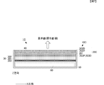
- FIG. 5 is a cross-sectional view of a display panel with a pressure sensor according to a third embodiment of the present invention.
- FIG. 6 is a plan view of a pressure sensor and a position detection sensor according to the third embodiment of the present invention.
- the display panel with a pressure sensor 10 ⁇ / b> B of the present embodiment includes a position detection sensor 70.
- the position detection sensor 70 and the pressure sensor 20 are disposed between the surface polarizing plate 302 and the liquid crystal panel 301.
- the position detection sensor 70 is disposed closer to the surface polarizing plate 302 than the pressing sensor 20.
- An intermediate member 270 is disposed between the position detection sensor 70 and the pressure sensor 20.
- the intermediate member 270 has insulating properties, translucency, and adhesiveness or tackiness.
- the position detection sensor 70 includes a flat insulating substrate 701 and a plurality of electrodes 702 and 703.
- the insulating substrate 701 is made of a light-transmitting material.
- the plurality of electrodes 702 are formed on one flat plate surface of the insulating substrate 701.
- the plurality of electrodes 702 are long and have a shape in which the long direction is along the Y direction.
- the plurality of electrodes 702 are arranged at intervals along the X direction.
- the plurality of electrodes 703 are formed on the other flat surface of the insulating substrate 701.
- the plurality of electrodes 703 are long and have a shape in which the long direction is along the X direction.
- the plurality of electrodes 703 are arranged at intervals along the Y direction.
- the plurality of electrodes 702 and 703 are made of a light-transmitting material, like the electrodes 202 and 203 of the pressure sensor 20 described above.
- the position detection sensor 70 detects a change in capacitance that occurs when an operator's finger comes close by the electrodes 702 and 703, and outputs this capacitance detection signal to the arithmetic circuit module 60.
- the arithmetic circuit module 60 detects the operation position from the combination of the electrodes 702 and 703 from which the capacitance detection signal is detected.
- the insulating substrate 701 further has birefringence.
- the position detection sensor 70 is formed so that the birefringence of the insulating substrate 701 compensates for the birefringence of the piezoelectric film 201 and cancels out.
- a desired color displayed on the display panel can be provided to the operator as in the first embodiment described above. Furthermore, by using the configuration of the present embodiment, it is possible to detect not only the push amount but also the operation position.
- the insulating substrate 701 of the position detection sensor 70 may be formed from a material having no birefringence, and the piezoelectric film 204 for phase compensation may be disposed as shown in the first embodiment. However, if the configuration of this embodiment is used, the piezoelectric film for phase compensation can be omitted, so that the display panel with pressure sensor 10B can be formed thinner.
- the position detection sensor 70 may be disposed on the liquid crystal panel 301 side of the pressing sensor 20.
- FIG. 7 is a cross-sectional view of a display panel with a pressure sensor according to a fourth embodiment of the present invention.
- the display panel 10C with a pressure sensor of this embodiment includes a pressure sensor 20C.
- the pressure sensor 20 ⁇ / b> C includes a piezoelectric film 201.
- a piezoelectric detection electrode 202P and a capacitance detection electrode 202D are formed on the first flat plate surface of the piezoelectric film 201.
- the piezoelectric detection electrode 202P and the capacitance detection electrode 202D are formed in a predetermined pattern.
- the piezoelectric detection electrode 202P and the capacitance detection electrode 202D are formed so as not to conduct each other.
- a piezoelectric detection electrode 203P and a capacitance detection electrode 203D are formed on the second flat plate surface of the piezoelectric film 201.
- the piezoelectric detection electrode 203P and the capacitance detection electrode 203D are formed in a predetermined pattern.
- the piezoelectric detection electrode 203P and the capacitance detection electrode 203D are formed so as not to conduct each other.
- the piezoelectric detection electrodes 202P and 203P are formed in a shape capable of detecting a voltage due to charges generated by the bending of the piezoelectric film 201.
- the capacitance detection electrodes 202D and 203D are formed in a shape capable of detecting a change in capacitance caused by an operation of the operator on the operation surface.
- the piezoelectric detection electrodes 202P and 203P and the capacitance detection electrodes 202D and 203D are made of a light-transmitting material.
- the desired color displayed on the display panel can be provided to the operator as in the above-described embodiments. Furthermore, a display panel with a pressure sensor and an electronic device with a pressure input function capable of detecting the push-in amount and the operation position can be formed thin.
- FIG. 8 is a diagram illustrating the relationship between the stretching directions in a state where four piezoelectric films are stacked (overlapped).
- the stretching directions 901 and 904 of the two piezoelectric films forming the first pair are orthogonal to each other.
- the stretching directions 911 and 912 of the two piezoelectric films forming the second pair are orthogonal to each other.
- the plurality of films having birefringence may be disposed between the front polarizing plate and the liquid crystal panel or between the liquid crystal panel and the rear polarizing plate. Even with such a configuration, a desired color displayed on the display panel can be provided to the operator as in the above-described embodiment.
- PLA and PLLA have been described as examples of the chiral polymer piezoelectric film.
- the above-described configuration is also applied when using other birefringent piezoelectric films such as PDLA. can do.
- 1, 1A, 1B, 1C electronic device with press input function
- 10, 10A, 10B, 10C display panel with pressure sensor, 20, 20C: pressure sensor, 30: display panel
- 40 protective member
- 50 housing
- 60 arithmetic circuit module
- 70 position detection sensor
- 201 Piezoelectric film
- 202, 203 electrodes
- 204 Piezoelectric film
- 202P 203P
- 202D, 203D Capacitance detection electrodes
- 301 Liquid crystal panel
- 302 Surface polarizing plate
- 701 an insulating substrate
- 702 and 703 Electrodes
Landscapes
- Physics & Mathematics (AREA)
- Engineering & Computer Science (AREA)
- Nonlinear Science (AREA)
- General Physics & Mathematics (AREA)
- Theoretical Computer Science (AREA)
- General Engineering & Computer Science (AREA)
- Chemical & Material Sciences (AREA)
- Crystallography & Structural Chemistry (AREA)
- Optics & Photonics (AREA)
- Mathematical Physics (AREA)
- Human Computer Interaction (AREA)
- Liquid Crystal (AREA)
- Devices For Indicating Variable Information By Combining Individual Elements (AREA)
- Position Input By Displaying (AREA)
- Polarising Elements (AREA)
Priority Applications (4)
| Application Number | Priority Date | Filing Date | Title |
|---|---|---|---|
| CN201480006134.2A CN104956244B (zh) | 2013-02-01 | 2014-01-24 | 带按压传感器的显示面板及带按压输入功能的电子设备 |
| JP2014559649A JP5860980B2 (ja) | 2013-02-01 | 2014-01-24 | 押圧センサ付き表示パネル、および押圧入力機能付き電子機器 |
| EP14746589.2A EP2952940B1 (de) | 2013-02-01 | 2014-01-24 | Anzeigetafel mit presssensor und elektronische vorrichtung mit presseingabefunktion |
| US14/813,247 US9990072B2 (en) | 2013-02-01 | 2015-07-30 | Display panel with pressure sensor and electronic device with pressing input function |
Applications Claiming Priority (2)
| Application Number | Priority Date | Filing Date | Title |
|---|---|---|---|
| JP2013-018770 | 2013-02-01 | ||
| JP2013018770 | 2013-02-01 |
Related Child Applications (1)
| Application Number | Title | Priority Date | Filing Date |
|---|---|---|---|
| US14/813,247 Continuation US9990072B2 (en) | 2013-02-01 | 2015-07-30 | Display panel with pressure sensor and electronic device with pressing input function |
Publications (1)
| Publication Number | Publication Date |
|---|---|
| WO2014119476A1 true WO2014119476A1 (ja) | 2014-08-07 |
Family
ID=51262190
Family Applications (1)
| Application Number | Title | Priority Date | Filing Date |
|---|---|---|---|
| PCT/JP2014/051457 Ceased WO2014119476A1 (ja) | 2013-02-01 | 2014-01-24 | 押圧センサ付き表示パネル、および押圧入力機能付き電子機器 |
Country Status (5)
| Country | Link |
|---|---|
| US (1) | US9990072B2 (de) |
| EP (1) | EP2952940B1 (de) |
| JP (1) | JP5860980B2 (de) |
| CN (1) | CN104956244B (de) |
| WO (1) | WO2014119476A1 (de) |
Cited By (2)
| Publication number | Priority date | Publication date | Assignee | Title |
|---|---|---|---|---|
| WO2017010495A1 (ja) * | 2015-07-15 | 2017-01-19 | 株式会社村田製作所 | 圧電センサ、タッチパネル、タッチ式入力装置および表示装置 |
| CN110494725A (zh) * | 2017-10-03 | 2019-11-22 | 株式会社村田制作所 | 按压传感器和电子设备 |
Families Citing this family (28)
| Publication number | Priority date | Publication date | Assignee | Title |
|---|---|---|---|---|
| US8487759B2 (en) | 2009-09-30 | 2013-07-16 | Apple Inc. | Self adapting haptic device |
| WO2015047372A1 (en) | 2013-09-30 | 2015-04-02 | Pearl Capital Developments Llc | Magnetic actuators for haptic response |
| US9317118B2 (en) | 2013-10-22 | 2016-04-19 | Apple Inc. | Touch surface for simulating materials |
| US10276001B2 (en) | 2013-12-10 | 2019-04-30 | Apple Inc. | Band attachment mechanism with haptic response |
| AU2014391723B2 (en) | 2014-04-21 | 2018-04-05 | Apple Inc. | Apportionment of forces for multi-touch input devices of electronic devices |
| US9830782B2 (en) | 2014-09-02 | 2017-11-28 | Apple Inc. | Haptic notifications |
| GB2533667B (en) | 2014-12-23 | 2017-07-19 | Cambridge Touch Tech Ltd | Pressure-sensitive touch panel |
| CN113655915B (zh) | 2014-12-23 | 2024-11-12 | 剑桥触控科技有限公司 | 压敏触摸面板 |
| US10353467B2 (en) | 2015-03-06 | 2019-07-16 | Apple Inc. | Calibration of haptic devices |
| AU2016100399B4 (en) | 2015-04-17 | 2017-02-02 | Apple Inc. | Contracting and elongating materials for providing input and output for an electronic device |
| CN107925333B (zh) | 2015-09-08 | 2020-10-23 | 苹果公司 | 用于在电子设备中使用的线性致动器 |
| GB2544353B (en) | 2015-12-23 | 2018-02-21 | Cambridge Touch Tech Ltd | Pressure-sensitive touch panel |
| US10282046B2 (en) | 2015-12-23 | 2019-05-07 | Cambridge Touch Technologies Ltd. | Pressure-sensitive touch panel |
| KR101877503B1 (ko) * | 2015-12-24 | 2018-07-11 | 주식회사 모다이노칩 | 복합 소자 및 이를 구비하는 전자기기 |
| US10039080B2 (en) | 2016-03-04 | 2018-07-31 | Apple Inc. | Situationally-aware alerts |
| US10268272B2 (en) | 2016-03-31 | 2019-04-23 | Apple Inc. | Dampening mechanical modes of a haptic actuator using a delay |
| CN106066732B (zh) * | 2016-05-30 | 2019-01-25 | 京东方科技集团股份有限公司 | 触摸屏及触摸显示装置 |
| CN106950742B (zh) * | 2017-05-24 | 2019-08-27 | 京东方科技集团股份有限公司 | 一种曲面显示装置及其制作方法 |
| US10622538B2 (en) | 2017-07-18 | 2020-04-14 | Apple Inc. | Techniques for providing a haptic output and sensing a haptic input using a piezoelectric body |
| US11093088B2 (en) | 2017-08-08 | 2021-08-17 | Cambridge Touch Technologies Ltd. | Device for processing signals from a pressure-sensing touch panel |
| GB2565305A (en) | 2017-08-08 | 2019-02-13 | Cambridge Touch Tech Ltd | Device for processing signals from a pressure-sensing touch panel |
| US10599223B1 (en) | 2018-09-28 | 2020-03-24 | Apple Inc. | Button providing force sensing and/or haptic output |
| US10691211B2 (en) | 2018-09-28 | 2020-06-23 | Apple Inc. | Button providing force sensing and/or haptic output |
| US11380470B2 (en) | 2019-09-24 | 2022-07-05 | Apple Inc. | Methods to control force in reluctance actuators based on flux related parameters |
| US11977683B2 (en) | 2021-03-12 | 2024-05-07 | Apple Inc. | Modular systems configured to provide localized haptic feedback using inertial actuators |
| US11809631B2 (en) | 2021-09-21 | 2023-11-07 | Apple Inc. | Reluctance haptic engine for an electronic device |
| JP7755142B2 (ja) * | 2021-10-27 | 2025-10-16 | 株式会社デンソーウェーブ | 光学的情報読取装置 |
| FR3160239B1 (fr) * | 2024-03-18 | 2026-04-24 | Commissariat A L Energie Atomique Et Aux Energies Alternatives | Dispositif de mesure de force en compression à sensibilité adaptable |
Citations (4)
| Publication number | Priority date | Publication date | Assignee | Title |
|---|---|---|---|---|
| JP2007086959A (ja) * | 2005-09-21 | 2007-04-05 | Matsushita Electric Ind Co Ltd | タッチパネル |
| WO2011125408A1 (ja) * | 2010-04-09 | 2011-10-13 | 株式会社村田製作所 | タッチパネルおよびタッチパネルを備える入出力装置 |
| JP2012214056A (ja) * | 2006-04-17 | 2012-11-08 | Mitsubishi Gas Chemical Co Inc | 透明導電性フィルム、およびそれを用いた低反射タッチパネル |
| JP2012230657A (ja) | 2011-04-13 | 2012-11-22 | Japan Display West Co Ltd | 表示パネル、駆動回路、駆動方法、および電子機器 |
Family Cites Families (28)
| Publication number | Priority date | Publication date | Assignee | Title |
|---|---|---|---|---|
| US4516112A (en) * | 1982-02-22 | 1985-05-07 | Eaton Corporation | Transparent touch switching system |
| JPS61175720A (ja) * | 1985-01-30 | 1986-08-07 | Ricoh Co Ltd | 情報入力表示素子 |
| DE69932826T2 (de) * | 1998-06-18 | 2006-12-14 | Kaneka Corp. | Transparentes touch panel und flüssigkristalldisplay mit einem transparenten touch panel |
| JP2006278034A (ja) * | 2005-03-28 | 2006-10-12 | Asahi Kasei Chemicals Corp | タッチパネル材料 |
| JP4412288B2 (ja) * | 2006-01-26 | 2010-02-10 | セイコーエプソン株式会社 | 電気光学装置及び電子機器 |
| JP4927159B2 (ja) * | 2007-03-01 | 2012-05-09 | シャープ株式会社 | 表示パネル用基板、表示パネル、表示装置、および表示パネル用基板の製造方法 |
| US9122092B2 (en) * | 2007-06-22 | 2015-09-01 | Google Technology Holdings LLC | Colored morphing apparatus for an electronic device |
| US8077154B2 (en) * | 2007-08-13 | 2011-12-13 | Motorola Mobility, Inc. | Electrically non-interfering printing for electronic devices having capacitive touch sensors |
| EP2221712A4 (de) * | 2007-12-14 | 2012-04-04 | Kyocera Corp | Berührungsbildschirm und anzeigevorrichtung mit berührungsbildschirm |
| JP5473905B2 (ja) * | 2008-05-12 | 2014-04-16 | 学校法人 関西大学 | 圧電素子および音響機器 |
| US20100103115A1 (en) * | 2008-10-24 | 2010-04-29 | Sony Ericsson Mobile Communications Ab | Display arrangement and electronic device |
| US8373667B2 (en) * | 2008-11-05 | 2013-02-12 | Massachusetts Institute Of Technology | Flat panel display with capacitance sensing touch screen |
| TWI478016B (zh) * | 2008-12-24 | 2015-03-21 | Prime View Int Co Ltd | 觸控式顯示裝置及其製造方法 |
| KR101022065B1 (ko) * | 2009-01-16 | 2011-03-17 | 삼성모바일디스플레이주식회사 | 터치 스크린 패널 |
| WO2010131551A1 (ja) * | 2009-05-11 | 2010-11-18 | 京セラ株式会社 | タッチパネル、およびこれを備えた表示装置 |
| JP5529456B2 (ja) * | 2009-07-31 | 2014-06-25 | 帝人株式会社 | ポリ乳酸フィルムおよびその製造方法 |
| WO2011156447A1 (en) * | 2010-06-11 | 2011-12-15 | 3M Innovative Properties Company | Positional touch sensor with force measurement |
| US20120127136A1 (en) * | 2010-08-18 | 2012-05-24 | Kent Displays Incorporated | Display device including piezoelectric and liquid crystal layers |
| CN102484199B (zh) * | 2010-08-25 | 2014-09-10 | 三井化学株式会社 | 高分子压电材料和其制造方法 |
| JP5131939B2 (ja) * | 2010-08-26 | 2013-01-30 | 株式会社村田製作所 | 圧電デバイス |
| JP5580155B2 (ja) * | 2010-09-27 | 2014-08-27 | スタンレー電気株式会社 | タッチパネル入力装置の製造方法 |
| JP5676216B2 (ja) * | 2010-11-11 | 2015-02-25 | 日本碍子株式会社 | 圧電素子の製造方法 |
| EP2696163B1 (de) * | 2011-04-08 | 2018-05-23 | Murata Manufacturing Co., Ltd. | Verschiebungssensor, verschiebungsdetektionsvorrichtung und betriebsvorrichtung |
| US8561080B2 (en) | 2011-04-26 | 2013-10-15 | Sap Ag | High-load business process scalability |
| US8723824B2 (en) * | 2011-09-27 | 2014-05-13 | Apple Inc. | Electronic devices with sidewall displays |
| US9136461B2 (en) * | 2011-10-13 | 2015-09-15 | Mitsui Chemicals, Inc. | Polymeric piezoelectric material and process for producing the same |
| US8773395B2 (en) * | 2012-04-24 | 2014-07-08 | Eastman Kodak Company | Touch-responsive capacitor with polarizing dielectric method |
| WO2014112494A1 (ja) * | 2013-01-18 | 2014-07-24 | 株式会社村田製作所 | 変位検出センサおよび操作入力装置 |
-
2014
- 2014-01-24 EP EP14746589.2A patent/EP2952940B1/de active Active
- 2014-01-24 CN CN201480006134.2A patent/CN104956244B/zh active Active
- 2014-01-24 JP JP2014559649A patent/JP5860980B2/ja active Active
- 2014-01-24 WO PCT/JP2014/051457 patent/WO2014119476A1/ja not_active Ceased
-
2015
- 2015-07-30 US US14/813,247 patent/US9990072B2/en active Active
Patent Citations (4)
| Publication number | Priority date | Publication date | Assignee | Title |
|---|---|---|---|---|
| JP2007086959A (ja) * | 2005-09-21 | 2007-04-05 | Matsushita Electric Ind Co Ltd | タッチパネル |
| JP2012214056A (ja) * | 2006-04-17 | 2012-11-08 | Mitsubishi Gas Chemical Co Inc | 透明導電性フィルム、およびそれを用いた低反射タッチパネル |
| WO2011125408A1 (ja) * | 2010-04-09 | 2011-10-13 | 株式会社村田製作所 | タッチパネルおよびタッチパネルを備える入出力装置 |
| JP2012230657A (ja) | 2011-04-13 | 2012-11-22 | Japan Display West Co Ltd | 表示パネル、駆動回路、駆動方法、および電子機器 |
Non-Patent Citations (1)
| Title |
|---|
| See also references of EP2952940A4 * |
Cited By (5)
| Publication number | Priority date | Publication date | Assignee | Title |
|---|---|---|---|---|
| WO2017010495A1 (ja) * | 2015-07-15 | 2017-01-19 | 株式会社村田製作所 | 圧電センサ、タッチパネル、タッチ式入力装置および表示装置 |
| JPWO2017010495A1 (ja) * | 2015-07-15 | 2018-03-29 | 株式会社村田製作所 | 表示装置 |
| US10528202B2 (en) | 2015-07-15 | 2020-01-07 | Murata Manufacturing Co., Ltd. | Piezoelectric sensor, touch panel, touch input device, and display device |
| CN110494725A (zh) * | 2017-10-03 | 2019-11-22 | 株式会社村田制作所 | 按压传感器和电子设备 |
| CN110494725B (zh) * | 2017-10-03 | 2021-04-20 | 株式会社村田制作所 | 按压传感器和电子设备 |
Also Published As
| Publication number | Publication date |
|---|---|
| EP2952940B1 (de) | 2019-05-22 |
| CN104956244B (zh) | 2017-07-21 |
| CN104956244A (zh) | 2015-09-30 |
| EP2952940A1 (de) | 2015-12-09 |
| EP2952940A4 (de) | 2016-08-24 |
| US20150338981A1 (en) | 2015-11-26 |
| US9990072B2 (en) | 2018-06-05 |
| JP5860980B2 (ja) | 2016-02-16 |
| JPWO2014119476A1 (ja) | 2017-01-26 |
Similar Documents
| Publication | Publication Date | Title |
|---|---|---|
| JP5860980B2 (ja) | 押圧センサ付き表示パネル、および押圧入力機能付き電子機器 | |
| JP6069500B2 (ja) | 押圧センサ付き表示パネル、および押圧入力機能付き電子機器 | |
| JP5871111B1 (ja) | タッチパネルおよび電子機器 | |
| CN105164621B (zh) | 触摸式输入装置以及显示装置 | |
| JP6179635B2 (ja) | タッチセンサ | |
| CN105593798A (zh) | 触摸传感器 | |
| WO2015041197A1 (ja) | 押圧センサ、タッチセンサ、押圧センサ付き表示パネル、およびタッチセンサ付き表示パネル | |
| US10101220B2 (en) | Displacement detection sensor and operation input device | |
| JP5939319B2 (ja) | 押圧センサ付き表示パネル、および押圧入力機能付き電子機器 | |
| US10528202B2 (en) | Piezoelectric sensor, touch panel, touch input device, and display device | |
| JP6132076B2 (ja) | 押圧検知タッチパネルおよび表示装置 |
Legal Events
| Date | Code | Title | Description |
|---|---|---|---|
| 121 | Ep: the epo has been informed by wipo that ep was designated in this application |
Ref document number: 14746589 Country of ref document: EP Kind code of ref document: A1 |
|
| ENP | Entry into the national phase |
Ref document number: 2014559649 Country of ref document: JP Kind code of ref document: A |
|
| NENP | Non-entry into the national phase |
Ref country code: DE |
|
| WWE | Wipo information: entry into national phase |
Ref document number: 2014746589 Country of ref document: EP |