WO2014119668A1 - 赤外線反射フィルムの製造方法 - Google Patents
赤外線反射フィルムの製造方法 Download PDFInfo
- Publication number
- WO2014119668A1 WO2014119668A1 PCT/JP2014/052132 JP2014052132W WO2014119668A1 WO 2014119668 A1 WO2014119668 A1 WO 2014119668A1 JP 2014052132 W JP2014052132 W JP 2014052132W WO 2014119668 A1 WO2014119668 A1 WO 2014119668A1
- Authority
- WO
- WIPO (PCT)
- Prior art keywords
- layer
- metal
- metal oxide
- target
- infrared reflective
- Prior art date
- Legal status (The legal status is an assumption and is not a legal conclusion. Google has not performed a legal analysis and makes no representation as to the accuracy of the status listed.)
- Ceased
Links
Images


Classifications
-
- H—ELECTRICITY
- H01—ELECTRIC ELEMENTS
- H01J—ELECTRIC DISCHARGE TUBES OR DISCHARGE LAMPS
- H01J37/00—Discharge tubes with provision for introducing objects or material to be exposed to the discharge, e.g. for the purpose of examination or processing thereof
- H01J37/32—Gas-filled discharge tubes
- H01J37/34—Gas-filled discharge tubes operating with cathodic sputtering
- H01J37/3411—Constructional aspects of the reactor
- H01J37/3414—Targets
- H01J37/3426—Material
- H01J37/3429—Plural materials
-
- G—PHYSICS
- G02—OPTICS
- G02B—OPTICAL ELEMENTS, SYSTEMS OR APPARATUS
- G02B5/00—Optical elements other than lenses
- G02B5/20—Filters
- G02B5/26—Reflecting filters
-
- B—PERFORMING OPERATIONS; TRANSPORTING
- B32—LAYERED PRODUCTS
- B32B—LAYERED PRODUCTS, i.e. PRODUCTS BUILT-UP OF STRATA OF FLAT OR NON-FLAT, e.g. CELLULAR OR HONEYCOMB, FORM
- B32B38/00—Ancillary operations in connection with laminating processes
- B32B38/0008—Electrical discharge treatment, e.g. corona, plasma treatment; wave energy or particle radiation
-
- C—CHEMISTRY; METALLURGY
- C23—COATING METALLIC MATERIAL; COATING MATERIAL WITH METALLIC MATERIAL; CHEMICAL SURFACE TREATMENT; DIFFUSION TREATMENT OF METALLIC MATERIAL; COATING BY VACUUM EVAPORATION, BY SPUTTERING, BY ION IMPLANTATION OR BY CHEMICAL VAPOUR DEPOSITION, IN GENERAL; INHIBITING CORROSION OF METALLIC MATERIAL OR INCRUSTATION IN GENERAL
- C23C—COATING METALLIC MATERIAL; COATING MATERIAL WITH METALLIC MATERIAL; SURFACE TREATMENT OF METALLIC MATERIAL BY DIFFUSION INTO THE SURFACE, BY CHEMICAL CONVERSION OR SUBSTITUTION; COATING BY VACUUM EVAPORATION, BY SPUTTERING, BY ION IMPLANTATION OR BY CHEMICAL VAPOUR DEPOSITION, IN GENERAL
- C23C14/00—Coating by vacuum evaporation, by sputtering or by ion implantation of the coating forming material
- C23C14/06—Coating by vacuum evaporation, by sputtering or by ion implantation of the coating forming material characterised by the coating material
- C23C14/08—Oxides
- C23C14/086—Oxides of zinc, germanium, cadmium, indium, tin, thallium or bismuth
-
- C—CHEMISTRY; METALLURGY
- C23—COATING METALLIC MATERIAL; COATING MATERIAL WITH METALLIC MATERIAL; CHEMICAL SURFACE TREATMENT; DIFFUSION TREATMENT OF METALLIC MATERIAL; COATING BY VACUUM EVAPORATION, BY SPUTTERING, BY ION IMPLANTATION OR BY CHEMICAL VAPOUR DEPOSITION, IN GENERAL; INHIBITING CORROSION OF METALLIC MATERIAL OR INCRUSTATION IN GENERAL
- C23C—COATING METALLIC MATERIAL; COATING MATERIAL WITH METALLIC MATERIAL; SURFACE TREATMENT OF METALLIC MATERIAL BY DIFFUSION INTO THE SURFACE, BY CHEMICAL CONVERSION OR SUBSTITUTION; COATING BY VACUUM EVAPORATION, BY SPUTTERING, BY ION IMPLANTATION OR BY CHEMICAL VAPOUR DEPOSITION, IN GENERAL
- C23C14/00—Coating by vacuum evaporation, by sputtering or by ion implantation of the coating forming material
- C23C14/06—Coating by vacuum evaporation, by sputtering or by ion implantation of the coating forming material characterised by the coating material
- C23C14/14—Metallic material, boron or silicon
- C23C14/20—Metallic material, boron or silicon on organic substrates
- C23C14/205—Metallic material, boron or silicon on organic substrates by cathodic sputtering
-
- C—CHEMISTRY; METALLURGY
- C23—COATING METALLIC MATERIAL; COATING MATERIAL WITH METALLIC MATERIAL; CHEMICAL SURFACE TREATMENT; DIFFUSION TREATMENT OF METALLIC MATERIAL; COATING BY VACUUM EVAPORATION, BY SPUTTERING, BY ION IMPLANTATION OR BY CHEMICAL VAPOUR DEPOSITION, IN GENERAL; INHIBITING CORROSION OF METALLIC MATERIAL OR INCRUSTATION IN GENERAL
- C23C—COATING METALLIC MATERIAL; COATING MATERIAL WITH METALLIC MATERIAL; SURFACE TREATMENT OF METALLIC MATERIAL BY DIFFUSION INTO THE SURFACE, BY CHEMICAL CONVERSION OR SUBSTITUTION; COATING BY VACUUM EVAPORATION, BY SPUTTERING, BY ION IMPLANTATION OR BY CHEMICAL VAPOUR DEPOSITION, IN GENERAL
- C23C14/00—Coating by vacuum evaporation, by sputtering or by ion implantation of the coating forming material
- C23C14/22—Coating by vacuum evaporation, by sputtering or by ion implantation of the coating forming material characterised by the process of coating
- C23C14/34—Sputtering
-
- C—CHEMISTRY; METALLURGY
- C23—COATING METALLIC MATERIAL; COATING MATERIAL WITH METALLIC MATERIAL; CHEMICAL SURFACE TREATMENT; DIFFUSION TREATMENT OF METALLIC MATERIAL; COATING BY VACUUM EVAPORATION, BY SPUTTERING, BY ION IMPLANTATION OR BY CHEMICAL VAPOUR DEPOSITION, IN GENERAL; INHIBITING CORROSION OF METALLIC MATERIAL OR INCRUSTATION IN GENERAL
- C23C—COATING METALLIC MATERIAL; COATING MATERIAL WITH METALLIC MATERIAL; SURFACE TREATMENT OF METALLIC MATERIAL BY DIFFUSION INTO THE SURFACE, BY CHEMICAL CONVERSION OR SUBSTITUTION; COATING BY VACUUM EVAPORATION, BY SPUTTERING, BY ION IMPLANTATION OR BY CHEMICAL VAPOUR DEPOSITION, IN GENERAL
- C23C14/00—Coating by vacuum evaporation, by sputtering or by ion implantation of the coating forming material
- C23C14/22—Coating by vacuum evaporation, by sputtering or by ion implantation of the coating forming material characterised by the process of coating
- C23C14/34—Sputtering
- C23C14/3407—Cathode assembly for sputtering apparatus, e.g. Target
- C23C14/3414—Metallurgical or chemical aspects of target preparation, e.g. casting, powder metallurgy
-
- G—PHYSICS
- G02—OPTICS
- G02B—OPTICAL ELEMENTS, SYSTEMS OR APPARATUS
- G02B5/00—Optical elements other than lenses
- G02B5/20—Filters
- G02B5/208—Filters for use with infrared or ultraviolet radiation, e.g. for separating visible light from infrared and/or ultraviolet radiation
-
- B—PERFORMING OPERATIONS; TRANSPORTING
- B29—WORKING OF PLASTICS; WORKING OF SUBSTANCES IN A PLASTIC STATE IN GENERAL
- B29L—INDEXING SCHEME ASSOCIATED WITH SUBCLASS B29C, RELATING TO PARTICULAR ARTICLES
- B29L2011/00—Optical elements, e.g. lenses, prisms
- B29L2011/0083—Reflectors
-
- B—PERFORMING OPERATIONS; TRANSPORTING
- B32—LAYERED PRODUCTS
- B32B—LAYERED PRODUCTS, i.e. PRODUCTS BUILT-UP OF STRATA OF FLAT OR NON-FLAT, e.g. CELLULAR OR HONEYCOMB, FORM
- B32B37/00—Methods or apparatus for laminating, e.g. by curing or by ultrasonic bonding
- B32B37/14—Methods or apparatus for laminating, e.g. by curing or by ultrasonic bonding characterised by the properties of the layers
- B32B37/24—Methods or apparatus for laminating, e.g. by curing or by ultrasonic bonding characterised by the properties of the layers with at least one layer not being coherent before laminating, e.g. made up from granular material sprinkled onto a substrate
- B32B2037/243—Coating
-
- B—PERFORMING OPERATIONS; TRANSPORTING
- B32—LAYERED PRODUCTS
- B32B—LAYERED PRODUCTS, i.e. PRODUCTS BUILT-UP OF STRATA OF FLAT OR NON-FLAT, e.g. CELLULAR OR HONEYCOMB, FORM
- B32B38/00—Ancillary operations in connection with laminating processes
- B32B2038/0052—Other operations not otherwise provided for
- B32B2038/0092—Metallizing
-
- B—PERFORMING OPERATIONS; TRANSPORTING
- B32—LAYERED PRODUCTS
- B32B—LAYERED PRODUCTS, i.e. PRODUCTS BUILT-UP OF STRATA OF FLAT OR NON-FLAT, e.g. CELLULAR OR HONEYCOMB, FORM
- B32B2309/00—Parameters for the laminating or treatment process; Apparatus details
- B32B2309/02—Temperature
-
- B—PERFORMING OPERATIONS; TRANSPORTING
- B32—LAYERED PRODUCTS
- B32B—LAYERED PRODUCTS, i.e. PRODUCTS BUILT-UP OF STRATA OF FLAT OR NON-FLAT, e.g. CELLULAR OR HONEYCOMB, FORM
- B32B2309/00—Parameters for the laminating or treatment process; Apparatus details
- B32B2309/04—Time
-
- B—PERFORMING OPERATIONS; TRANSPORTING
- B32—LAYERED PRODUCTS
- B32B—LAYERED PRODUCTS, i.e. PRODUCTS BUILT-UP OF STRATA OF FLAT OR NON-FLAT, e.g. CELLULAR OR HONEYCOMB, FORM
- B32B2309/00—Parameters for the laminating or treatment process; Apparatus details
- B32B2309/08—Dimensions, e.g. volume
- B32B2309/10—Dimensions, e.g. volume linear, e.g. length, distance, width
- B32B2309/105—Thickness
-
- B—PERFORMING OPERATIONS; TRANSPORTING
- B32—LAYERED PRODUCTS
- B32B—LAYERED PRODUCTS, i.e. PRODUCTS BUILT-UP OF STRATA OF FLAT OR NON-FLAT, e.g. CELLULAR OR HONEYCOMB, FORM
- B32B2309/00—Parameters for the laminating or treatment process; Apparatus details
- B32B2309/60—In a particular environment
- B32B2309/62—Inert
-
- B—PERFORMING OPERATIONS; TRANSPORTING
- B32—LAYERED PRODUCTS
- B32B—LAYERED PRODUCTS, i.e. PRODUCTS BUILT-UP OF STRATA OF FLAT OR NON-FLAT, e.g. CELLULAR OR HONEYCOMB, FORM
- B32B2309/00—Parameters for the laminating or treatment process; Apparatus details
- B32B2309/60—In a particular environment
- B32B2309/66—Fluid other than air
-
- B—PERFORMING OPERATIONS; TRANSPORTING
- B32—LAYERED PRODUCTS
- B32B—LAYERED PRODUCTS, i.e. PRODUCTS BUILT-UP OF STRATA OF FLAT OR NON-FLAT, e.g. CELLULAR OR HONEYCOMB, FORM
- B32B2310/00—Treatment by energy or chemical effects
- B32B2310/08—Treatment by energy or chemical effects by wave energy or particle radiation
- B32B2310/0806—Treatment by energy or chemical effects by wave energy or particle radiation using electromagnetic radiation
- B32B2310/0831—Treatment by energy or chemical effects by wave energy or particle radiation using electromagnetic radiation using UV radiation
-
- H—ELECTRICITY
- H01—ELECTRIC ELEMENTS
- H01J—ELECTRIC DISCHARGE TUBES OR DISCHARGE LAMPS
- H01J2237/00—Discharge tubes exposing object to beam, e.g. for analysis treatment, etching, imaging
- H01J2237/32—Processing objects by plasma generation
- H01J2237/33—Processing objects by plasma generation characterised by the type of processing
- H01J2237/332—Coating
Definitions
- the metal powder used for forming the target preferably contains metal zinc and / or metal tin.
- the total content of metal zinc and metal tin used for forming the target is preferably 0.1% by weight to 20% by weight.
- the ratio of zinc atoms and tin atoms contained in the target is preferably in the range of 10:90 to 60:40 in terms of atomic ratio.
- the metal oxide layer is formed continuously by 6000 nm ⁇ m or more in terms of the product of the film thickness and length (cross-sectional area in the MD direction).
- FIG. 1 is a cross-sectional view schematically showing a configuration example of an infrared reflecting film.
- the infrared reflective film 100 includes an infrared reflective layer 20 and a transparent protective layer 30 in this order on one main surface of the transparent film substrate 10.
- the thickness of the transparent film substrate 10 is not particularly limited, but a range of about 10 ⁇ m to 300 ⁇ m is suitable. Moreover, since processing at a high temperature may be performed when the infrared reflective layer 20 is formed on the transparent film substrate 10, the resin material constituting the transparent film substrate is preferably excellent in heat resistance. . Examples of the resin material constituting the transparent film substrate include polyethylene terephthalate (PET), polyethylene naphthalate (PEN), polyetheretherketone (PEEK), and polycarbonate (PC).
- PET polyethylene terephthalate
- PEN polyethylene naphthalate
- PEEK polyetheretherketone
- PC polycarbonate
- the amount of metal used for forming the sputter target is preferably 0.1% by weight to 20% by weight, more preferably 0.2% by weight to 15% by weight in the target forming material, and 0.5% More preferred is from 13% by weight to 13% by weight, and especially preferred is from 1% to 12% by weight.
- the metal powder used as a target forming material is oxidized by sintering, it may exist as a metal oxide in the sintered target.
- the content of Sn in the sputtering target is preferably 40 atomic percent or more, more preferably 50 atomic percent or more, and further preferably 60 atomic percent or more with respect to the total of 100 atomic percent of Sn and Zn.
- Sn-rich ZTO tends to have a low electrical conductivity.
- a target obtained by sintering a metal oxide and a metal powder is used to improve the electrical conductivity of the target. Therefore, Sn-rich ZTO can be formed by DC sputtering.
- Sputtering targets used for forming a metal oxide layer include zinc, tin, and oxides thereof, as well as metals such as Ti, Zr, Hf, Nb, Al, Ga, In, and Tl, or oxidation of these metals. You may contain a thing. However, when the content of metal atoms other than zinc and tin is increased, the durability of the infrared reflecting layer may be lowered and the transparency may be lowered. Therefore, out of a total of 100 atomic% of metals in the sputtering target used for metal oxide film formation, the total of zinc atoms and tin atoms is preferably 97 atomic% or more, and more preferably 99 atomic% or more.
- the sputtering deposition chamber In sputter deposition using such a target, it is preferable to first evacuate the sputtering deposition chamber to an atmosphere in which impurities such as moisture in the sputtering apparatus and organic gas generated from the substrate are removed.
- sputtering deposition is performed while introducing an inert gas such as Ar and oxygen into the sputtering deposition chamber.
- the amount of oxygen introduced into the film forming chamber is preferably 8% by volume or less, more preferably 5% by volume or less, and still more preferably 4% by volume or less with respect to the total flow rate of the introduced gas.
- the amount of oxygen introduced is the amount (% by volume) of oxygen relative to the total amount of gas introduced into the deposition chamber in which the target used for deposition of the metal oxide layer is disposed.
- the oxygen introduction amount is calculated based on the amount of gas introduced into each separated film forming chamber.
- the amount of oxygen introduced into the deposition chamber during sputtering deposition is preferably 0.1% by volume or more, more preferably 0.5% by volume or more, and even more preferably 1% by volume or more with respect to the total introduced gas flow rate. . *
- the substrate temperature when the metal oxide layer is formed by sputtering is preferably lower than the heat resistance temperature of the transparent film substrate.
- the substrate temperature is preferably 20 ° C. to 160 ° C., for example, and more preferably 30 ° C. to 140 ° C.
- Power density during sputtering film formation for example, 0.1 W / cm 2 ⁇ is preferably 10 W / cm 2, more preferably 0.5W / cm 2 ⁇ 7.5W / cm 2, 1W / cm 2 ⁇ 6W / cm 2 is more preferable.
- the process pressure during film formation is preferably, for example, 0.01 Pa to 10 Pa, more preferably 0.05 Pa to 5 Pa, and further preferably 0.1 Pa to 1 Pa. If the process pressure is too high, the film forming rate tends to decrease, whereas if the pressure is too low, the discharge tends to become unstable.
- the thickness of the metal oxide layers 21 and 22 takes into consideration the refractive index and thickness of the metal layer, the number of laminated infrared reflection layers, etc. so that the infrared reflection layer 20 transmits visible light and selectively reflects near infrared rays. And set appropriately.
- the thickness of each metal oxide layer can be adjusted in the range of, for example, about 3 nm to 100 nm, preferably about 5 nm to 80 nm.
- a transparent protective layer 30 is provided on the infrared reflective layer 20 for the purpose of preventing scratches and deterioration of the metal oxide layers 21 and 22 and the metal layer 25.
- the material and configuration of the transparent protective layer 30 are not limited, but those having a high visible light transmittance are preferably used.
- the transparent protective layer 30 has a small far-infrared absorptivity from a viewpoint of improving the heat insulation effect by an infrared reflective film.
- the thickness of the transparent protective layer is preferably 20 nm to 500 nm, more preferably 25 nm to 200 nm, still more preferably 30 nm to 150 nm, and 40 nm to 110 nm. Particularly preferred is 45 nm to 100 nm or less.
- the thickness of the transparent protective layer is excessively large, the heat insulating property of the infrared reflective film tends to be reduced due to an increase in far-infrared absorption in the transparent protective layer.
- a method for increasing the durability of the infrared reflective layer itself a method for increasing the content of components such as palladium in the metal layer 25 as described above can be used.
- the content of silver: palladium is preferably about 90:10 to 98: 2, more preferably about 92: 8 to 97: 3, by weight. More preferably, if it is about 93: 7 to 96: 4, even when the thickness of the transparent protective layer 30 is small, the deterioration of the metal layer 25 can be prevented and the durability of the infrared reflecting film can be enhanced.
- the material is preferably a material having high visible light transmittance and excellent mechanical strength and chemical strength.
- actinic ray curable or thermosetting organic resins such as fluorine, acrylic, urethane, ester, epoxy, and silicone, silicon oxide, silicon nitride, silicon oxynitride, aluminum oxide, titanium oxide,
- An inorganic material such as zirconium oxide or sialon (SiAlON) or an organic / inorganic hybrid material in which an organic component and an inorganic component are chemically bonded is preferably used.
- ester compounds having an acidic group and a polymerizable functional group in the same molecule include polyvalent acids such as phosphoric acid, sulfuric acid, oxalic acid, succinic acid, phthalic acid, fumaric acid, and maleic acid; And an ester of a compound having a polymerizable functional group such as a group, silanol group or epoxy group and a hydroxyl group in the molecule.
- the said ester compound may be polyvalent esters, such as a diester and a triester, it is preferable that at least 1 in the acidic group of a polyvalent acid is not esterified.
- the ester compound preferably contains a (meth) acryloyl group as a polymerizable functional group.
- the ester compound may have a plurality of polymerizable functional groups in the molecule.
- a phosphoric acid monoester compound or a phosphoric acid diester compound represented by the following formula (1) is preferably used.
- phosphoric acid monoester and phosphoric acid diester can also be used together.
- a compound having a small content such as a C ⁇ C bond, a C ⁇ O bond, a C—O bond or an aromatic ring is preferably used.
- a polyolefin such as polyethylene or polypropylene
- alicyclic polymers such as cycloolefin polymers, rubber polymers, and the like are preferably used.
- the material constituting the transparent protective layer in addition to having a low far-infrared absorptivity, materials having excellent adhesion to the infrared reflective layer and excellent scratch resistance are preferably used. From this point of view, rubber-based materials are particularly preferable, and nitrile rubber-based materials are particularly preferably used.
- the nitrile rubber-based material contains a structure represented by the following formulas (A), (B) and (C) in the molecule.
- R 1 is hydrogen or a methyl group
- R 2 to R 5 are each independently hydrogen, a linear or branched alkyl group having 1 to 4 carbon atoms, or A straight-chain or branched alkenyl group having 1 to 4 carbon atoms.
- nitrile rubber in which R 1 to R 5 are all hydrogen in the above formulas (A) to (C) is excellent in transparency and durability, and is suitable as a material for the transparent protective layer.
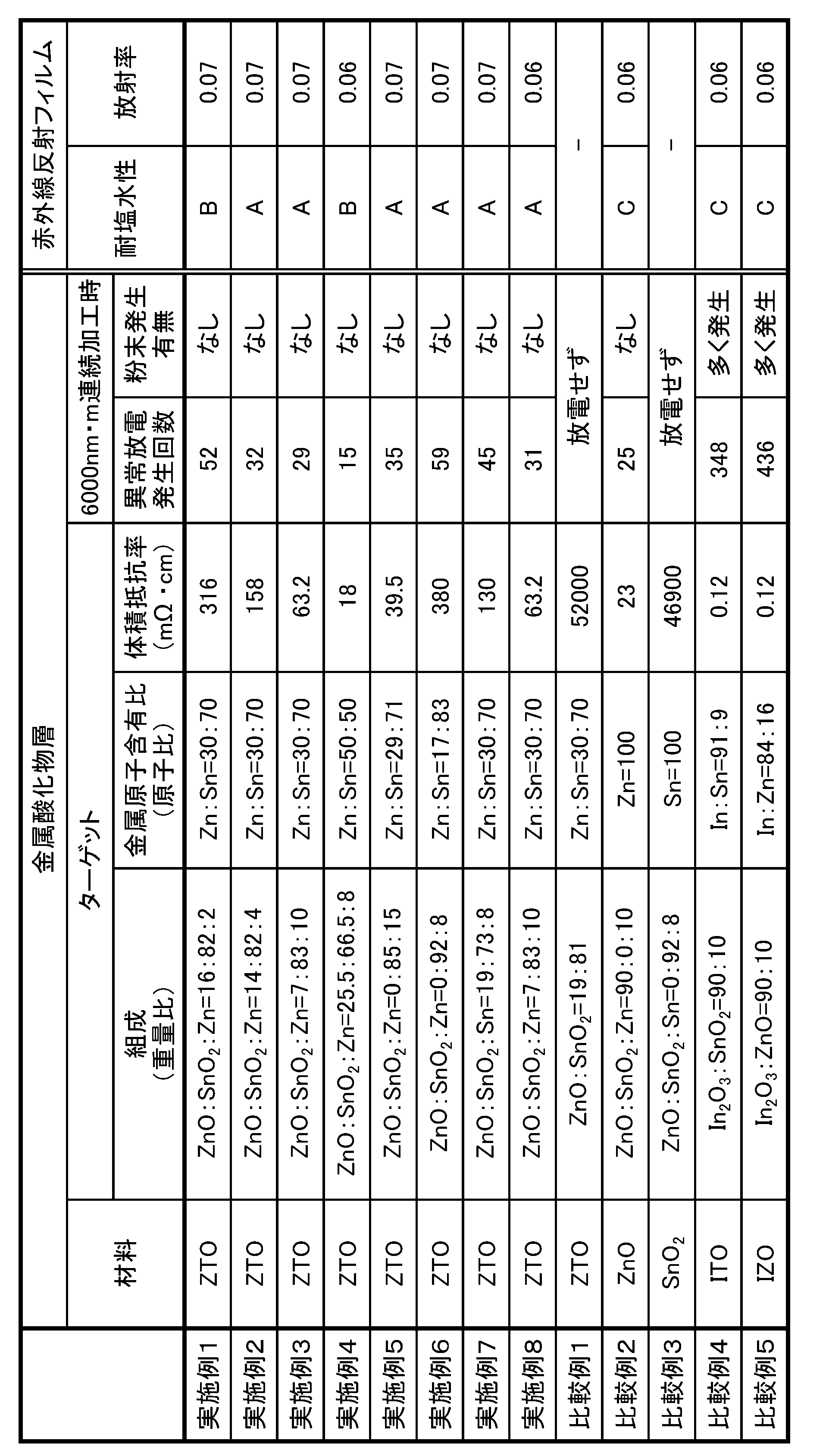
- sputter deposition was continuously performed over a length of 200 m in the winding direction (the product of the thickness and the length of the metal oxide layer was 6000 nm ⁇ m), but abnormal discharge occurred during sputtering. No causative powder was generated, and the film could be continuously formed stably without cleaning the target and the sputtering apparatus.
- the visible light transmittance of the infrared reflective film produced as described above was 70.1%.
- Example 5 As a sputtering target for forming the metal oxide layer, a target which did not have zinc oxide and was sintered with tin oxide: metal zinc powder at a weight ratio of 85:15 was used. The visible light transmittance of the infrared reflective film was 67.7%.
- a sputtering target for forming the metal oxide layer As a sputtering target for forming the metal oxide layer, a target having no metal powder and sintered with zinc oxide: tin oxide at a weight ratio of 19:81 was used. Other than that, sputter deposition was attempted under the same conditions as in Example 1, but no discharge with a DC power source occurred, and the metal oxide layer could not be deposited.
- Example 3 and Example 4 were compared, the durability of the infrared reflective film tended to decrease as the zinc atom content increased. According to this result, it is understood that tin-rich ZTO is preferably formed as the metal oxide layer from the viewpoint of enhancing the durability of the infrared reflective film.
- tin-rich ZTO is preferably formed as the metal oxide layer from the viewpoint of enhancing the durability of the infrared reflective film.
- Examples 2 and 3 containing zinc as a metal powder in the target and Example 7 containing tin are compared, if the metal content is the same, the volume resistivity of the target of zinc is higher. It appears to be small (high conductivity) and high visible light transmission. From this result, it can be said that in the present invention, it is particularly preferable that sputtering film formation is performed using a target containing metallic zinc as a target material.
Landscapes
- Chemical & Material Sciences (AREA)
- Physics & Mathematics (AREA)
- Engineering & Computer Science (AREA)
- Organic Chemistry (AREA)
- Chemical Kinetics & Catalysis (AREA)
- Materials Engineering (AREA)
- Mechanical Engineering (AREA)
- Metallurgy (AREA)
- General Physics & Mathematics (AREA)
- Optics & Photonics (AREA)
- Plasma & Fusion (AREA)
- Thermal Sciences (AREA)
- Health & Medical Sciences (AREA)
- Toxicology (AREA)
- Analytical Chemistry (AREA)
- Laminated Bodies (AREA)
- Optical Filters (AREA)
- Compositions Of Oxide Ceramics (AREA)
- Oxygen, Ozone, And Oxides In General (AREA)
- Physical Vapour Deposition (AREA)
Abstract
Description
透明フィルム基材10としては、可撓性の透明フィルムが用いられる。透明フィルム基材としては、可視光線透過率が80%以上のものが好適に用いられる。なお、可視光線透過率は、JIS A5759-2008(建築窓ガラスフィルム)に準じて測定される。
赤外線反射層20は、可視光を透過し、赤外線を反射するものであり、金属層および金属酸化物層を有する。一般に、赤外線反射層20は、図1に示すように、金属層25が、金属酸化物層21,22に挟持された構成を有する。なお、図1では、1層の金属層25が2層の金属酸化物層21,22に挟持された3層構成の赤外線反射層20が図示されているが、赤外線反射層は、例えば、金属酸化物層/金属層/金属酸化物層/金属層/金属酸化物層の5層構成とすることもできる。積層数を5層、7層、9層…と増加させるほど、反射率の波長選択性を高め、近赤外線の反射率を高めて遮熱性を持たせつつ、可視光線の透過率を高めることができる。一方、生産性を高める観点からは、赤外線反射層は、図1に示すような3層構成が好ましい。
金属層25は、赤外線反射の中心的な役割を有する。金属層25の材料としては、Au,Ag,Cu,Al等の金属、あるいはこれらの2種以上を含有する合金が用いられる。中でも、可視光線透過率と赤外線反射率を高める観点から、銀を主成分とするものが好適に用いられる。銀は高い自由電子密度を有するため、近赤外線・遠赤外線の高い反射率を実現することができ、赤外線反射層20を構成する層の積層数が少ない場合でも、遮熱効果および断熱効果に優れる赤外線反射フィルムが得られる。
金属酸化物層21,22は、金属層25との界面における可視光線の反射量を制御して、高い可視光線透過率と、赤外線反射率とを両立させる等の目的で設けられる。また、金属酸化物層は、金属層25の劣化を防止するための保護層としても機能し得る。赤外線反射層における反射および透過の波長選択性を高める観点から、金属酸化物層21,22の可視光に対する屈折率は、1.5以上が好ましく、1.6以上がより好ましく、1.7以上がさらに好ましい。上記の屈折率を有する材料としては、Ti,Zr,Hf,Nb,Zn,Al,Ga,In,Tl,Ga,Sn等の金属の酸化物、あるいはこれらの金属の複合酸化物が挙げられる。
赤外線反射層20上には、金属酸化物層21,22や金属層25の擦傷や劣化を防止する目的で、透明保護層30が設けられる。透明保護層30の材料や構成は限定されないが、高い可視光線透過率を有するものが好ましく用いられる。また、赤外線反射フィルムによる断熱効果を高める観点から、透明保護層30は、遠赤外線の吸収率が小さいことが好ましい。透明保護層30による遠赤外線の吸収率が大きいと、室内の遠赤外線が透明保護層で吸収され、熱伝導によって外部に放熱されるため、赤外線反射フィルムの断熱性が低下する傾向がある。一方、透明保護層30による遠赤外線吸収が少ない場合、遠赤外線は、赤外線反射層20の金属層25により室内に反射される。そのため、遠赤外線の吸収率が小さいほど、赤外線反射フィルムによる断熱効果が高められる。


上記のように、本発明の赤外線反射フィルム100は、透明フィルム基材10の一主面上に、金属層および金属酸化物層を含む赤外線反射層20、ならびに透明保護層30を有する。透明フィルム基材10と赤外線反射層20との間や、赤外線反射層と透明保護層との間には、各層の密着性を高める目的や、赤外線反射フィルムの強度を高める等の目的で、ハードコート層や易接着層等が設けられていてもよい。易接着層やハードコート層等の材料や形成方法は特に限定されないが、可視光線透過率の高い透明な材料が好適に用いられる。
本発明の赤外線反射フィルムは、透明保護層30側から測定した垂直放射率が、0.20以下であることが好ましく、0.15以下であることがより好ましく、0.12以下であることがさらに好ましく、0.10以下であることが特に好ましい。なお、垂直放射率は、JlS R3106:2008(板ガラス類の透過率・反射率・放射率・日射熱取得率の試験方法)に準じて測定される。赤外線反射フィルムが5重量%の塩化ナトリウム水溶液に5日間浸漬された後の放射率の変化は、0.02以下が好ましく、0.01以下がより好ましい。赤外線反射フィルムの可視光線透過率は、63%以上が好ましく、65%以上がより好ましく、67%以上がさらに好ましく、68%以上が特に好ましい。本発明においては、赤外線反射層20を構成する金属酸化物層として、ZTOが製膜されることによって、上記の可視光線透過率、垂直放射率および耐久性を同時に兼ね備える赤外線反射フィルムを高生産性で製造することができる。
本発明の赤外線反射フィルムは、建物や乗り物等の窓、植物等を入れる透明ケース、冷凍もしくは冷蔵のショーケース等に貼着し、冷暖房効果の向上や急激な温度変化を防ぐために、好ましく使用される。図2に模式的に示すように、本発明の赤外線反射フィルム100は、屋外からの可視光(VIS)を透過して室内に導入すると共に、屋外からの近赤外線(NIR)を赤外線反射層20で反射する。近赤外線反射により、太陽光等に起因する室外からの熱の室内への流入が抑制される(遮熱効果が発揮される)ため、夏場の冷房効率を高めることができる。さらに、透明保護層30として遠赤外線吸収の小さいものが用いられる場合、赤外線反射層20により、暖房器具80等から放射される室内の遠赤外線(FIR)が室内に反射されるため、断熱効果が発揮され、冬場の暖房効率を高めることができる。
<各層の厚み>
赤外線反射層を構成する各層の厚みは、集束イオンビーム加工観察装置(日立製作所製、製品名「FB-2100」)を用いて、集束イオンビーム(FIB)法により試料を加工し、その断面を、電界放出形透過電子顕微鏡(日立製作所製、製品名「HF-2000」)により観察して求めた。基材上に形成されたハードコート層、および透明保護層の厚みは、瞬間マルチ測光システム(大塚電子製、製品名「MCPD3000」)を用い、測定対象側から光を入射させた際の可視光の反射光の干渉パターンから、計算により求めた。なお、透明保護層の厚みが小さく、可視光域の干渉パターンの観察が困難なもの(厚み約150nm以下)については、上記赤外線反射層の各層と同様に、透過電子顕微鏡観察により厚みを求めた。
抵抗率計(三菱化学アナリテック製、製品名「ロレスタ」)を用いて、ターゲット表面の表面抵抗ρs(Ω/□)を測定し、表面抵抗ρsと膜厚の積から、体積抵抗率ρvを算出した。
スパッタ製膜時に、直流電源(HUTTINGER Elektronik製、商品名「TruPlasma DC3010」)に付属しているアークカウンターの数値をモニタリングし、異常放電発生時の瞬間的な電圧低下を読み取ることにより、異常放電の回数を調べた。
垂直放射率は、角度可変反射アクセサリを備えるフーリエ変換型赤外分光(FT-IR)装置(Varian製)を用いて、保護層側から赤外線を照射した場合の、波長5μm~25μmの赤外光の正反射率を測定し、JIS R3106-2008(板ガラス類の透過率・反射率・放射率・日射熱取得率の試験方法)に準じて求めた。
可視光線透過率は、分光光度計(日立ハイテク製 製品名「U-4100」)を用いて、JIS A5759-2008(建築窓ガラスフィルム)に準じて求めた。
赤外線反射フィルムの透明フィルム基材側の面を、厚み25μmの粘着剤層を介して3cm×3cmのガラス板に貼り合せたものを試料として用いた。この試料を5重量%の塩化ナトリウム水溶液に浸漬し、試料および塩化ナトリウム水溶液が入った容器を50℃の乾燥機に入れ、5日後および10日後に放射率の変化および外観の変化を確認し、以下の評価基準に従って評価した。
A:10日間浸漬後も外観変化がなく、かつ放射率の変化が0.02以下であるもの
B:5日間浸漬後は外観変化がなく、かつ放射率の変化が0.02以下であるが、10日間浸漬後は、外観変化が確認されるもの
C:5日間浸漬後に、外観の変化が確認され、放射率の変化が0.02以上であるもの
(基材へのハードコート層の形成)
厚みが50μmのポリエチレンテレフタレートフィルム(東レ製、商品名「ルミラー U48」、可視光線透過率93%)の一方の面に、アクリル系の紫外線硬化型ハードコート層(日本曹達製、NH2000G)が2μmの厚みで形成された。詳しくは、グラビアコーターにより、ハードコート溶液が塗布され、80℃で乾燥後、超高圧水銀ランプにより積算光量300mJ/cm2の紫外線が照射され、硬化が行われた。
ポリエチレンテレフタレートフィルム基材のハードコート層上に、巻取式スパッタ装置を用いて、赤外線反射層が形成された。詳しくは、DCマグネトロンスパッタ法により、亜鉛-錫複合酸化物(ZTO)からなる膜厚30nmの第一金属酸化物層、Ag-Pd合金からなる膜厚15nmの金属層、ZTOからなる膜厚30nmの第二金属酸化物層が順次形成された。ZTO金属酸化物層の形成には、酸化亜鉛と酸化錫と金属亜鉛粉末とを、16:82:2の重量比で焼結させたターゲットが用いられ、電力密度:2.67W/cm2、基板温度80℃の条件でスパッタが行われた。この際、スパッタ製膜室へのガス導入量は、Ar:O2が98:2(体積比)となるように調整された。金属層の形成には、銀:パラジウムを96.4:3.6の重量比で含有する金属ターゲットが用いられた。
赤外線反射層上に、リン酸エステル化合物に由来する架橋構造を有するフッ素系の紫外線硬化型樹脂からなる保護層が60nmの厚みで形成された。詳しくは、フッ素系ハードコート樹脂溶液(JSR製、商品名「JUA204」)の固形分100重量部に対して、リン酸エステル化合物(日本化薬製、商品名「KAYAMER PM-21」)を5重量部添加した溶液を、アプリケーターを用いて塗布し、60℃で1分間乾燥後、窒素雰囲気下で超高圧水銀ランプにより積算光量400mJ/cm2の紫外線が照射され、硬化が行われた。なお、上記リン酸エステル化合物は、分子中に1個のアクリロイル基を有するリン酸モノエステル化合物(前記の式(1)において、Xがメチル基、n=0、p=1である化合物)と分子中に2個のアクリロイル基を有するリン酸ジエステル化合物(前記の式(1)において、Xがメチル基、n=0、p=2である化合物)との混合物である。
以下の実施例2~7では、金属酸化物層製膜のためのターゲットの組成が変更されたこと以外は、いずれも実施例1と同様にして、赤外線反射フィルムが作製された。これらの実施例においては、いずれも実施例1と同様に、スパッタ中に異常放電の原因となる粉末が発生せず、ターゲットおよびスパッタ装置を清掃することなく、金属酸化物層の厚みと長さの積で6000nm・mにわたって、連続して安定した製膜を行うことができた。
金属酸化物層を形成するためのスパッタリングターゲットとして、酸化亜鉛:酸化錫:金属亜鉛粉末を、14:82:4の重量比で焼結させたターゲットが用いられた。赤外線反射フィルムの可視光線透過率は、69.8%であった。
金属酸化物層を形成するためのスパッタリングターゲットとして、酸化亜鉛:酸化錫:金属亜鉛粉末を、7:83:10の重量比で焼結させたターゲットが用いられた。赤外線反射フィルムの可視光線透過率は、68.6%であった。
[実施例4]
金属酸化物層を形成するためのスパッタリングターゲットとして、酸化亜鉛:酸化錫:金属亜鉛粉末を、25.5:66.5:8の重量比で焼結させたターゲットが用いられた。赤外線反射フィルムの可視光線透過率は、69.5%であった。
金属酸化物層を形成するためのスパッタリングターゲットとして、酸化亜鉛を有さず、酸化錫:金属亜鉛粉末を85:15の重量比で焼結させたターゲットが用いられた。赤外線反射フィルムの可視光線透過率は、67.7%であった。
金属酸化物層を形成するためのスパッタリングターゲットとして、酸化亜鉛を有さず、酸化錫:金属亜鉛粉末を92:8の重量比で焼結させたターゲットが用いられた。赤外線反射フィルムの可視光線透過率は、68.2%であった。
金属酸化物層を形成するためのスパッタリングターゲットとして、酸化亜鉛:酸化錫:金属錫粉末を、19:73:8の重量比で焼結させたターゲットが用いられた。赤外線反射フィルムの可視光線透過率は、67.5%であった。
金属層の形成において、Ag-Pd合金に代えて、銀:金を90:10の重量比で含有する金属ターゲットが用いられ、Ag-Au合金からなる金属層が形成された。それ以外は、実施例3と同様にして、赤外線反射フィルムが作製された。
金属酸化物層を形成するためのスパッタリングターゲットとして、金属粉末を有さず、酸化亜鉛:酸化錫を19:81の重量比で焼結させたターゲットが用いられた。それ以外は、実施例1と同様の条件でスパッタ製膜を試みたが、直流電源での放電が生じず、金属酸化物層を製膜することができなかった。
金属酸化物層を形成するためのスパッタリングターゲットとして、金属粉末を有さず、酸化亜鉛:酸化錫を90:10の重量比で焼結させたターゲットが用いられた。それ以外は、実施例1と同様の条件で赤外線反射フィルムが作製された。連続スパッタの製膜性は実施例1と同様に良好であったが、赤外線反射フィルムの可視光線透過率は、60.1%であり、上記各実施例に比して大幅に低下していた。また、赤外線反射フィルムの耐久性(耐塩水性)も低下していた。
金属酸化物層を形成するためのスパッタリングターゲットとして、酸化亜鉛および金属亜鉛を有さず、酸化錫:金属錫を92:8の重量比で焼結させたターゲットが用いられた。それ以外は、実施例1と同様の条件でスパッタ製膜を試みたが、直流電源での放電が生じず、金属酸化物層を製膜することができなかった。
比較例4では、第一金属酸化物層および第二金属酸化物層として、ZTOに代えて、酸化インジウム錫(ITO)が、それぞれ40nmの膜厚で製膜された。ITOの製膜には、酸化インジウム:酸化錫を90:10の重量比で焼結させたターゲットが用いられた。それ以外は、実施例1と同様の条件でスパッタ製膜を行ったところ、巻取方向に25mの長さ(金属酸化物層の厚みと長さの積で1000nm・m)まで連続製膜した段階から、異常放電の発生がみられた。6000nm・mを連続製膜した後、ターゲット表面を確認したところ、異常放電の原因となる粉末の付着がみられた。
比較例4では、第一金属酸化物層および第二金属酸化物層として、ZTOに代えて、酸化インジウム亜鉛(IZO)が、それぞれ40nmの膜厚で製膜された。IZOの製膜には、酸化インジウム:酸化亜鉛を90:10の重量比で焼結させたターゲットが用いられた。それ以外は、実施例1と同様の条件でスパッタ製膜を行ったところ、巻取方向に50mの長さ(金属酸化物層の厚みと長さの積で2000nm・m)まで連続製膜した段階から、異常放電の発生がみられた。6000nm・mを連続製膜した後、ターゲット表面を確認したところ、異常放電の原因となる粉末の付着がみられた。
上記各実施例および比較例の赤外線反射フィルムの金属酸化物層の材料、および製膜に用いられたターゲットの材料組成、ならびに赤外線反射フィルムの評価結果を表1に示す。実施例2、比較例4および比較例5(IZO)の金属酸化物層製膜時の異常放電発生回数を、製膜量に対してプロットしたグラフを図3に、6000nm・mを連続製膜後にターゲット表面を拭った際の粉末の付着状況を示す写真を図4に、それぞれ示す。図3および図4において、(A),(B)および(C)は、それぞれ、実施例2(ZTO),比較例4(ITO),および比較例5(IZO)の異常放電回数および粉末付着状況を表す。
10: 透明フィルム基材
20: 赤外線反射層
21,22: 金属酸化物層
25: 金属層
30: 保護層
60: 接着剤層
Claims (5)
- 透明フィルム基材上に、金属層および金属酸化物層を有する赤外線反射層と、透明保護層とをこの順に備える赤外線反射フィルムの製造方法であって、
前記金属酸化物層の製膜が、巻取式スパッタ装置を用いる直流スパッタ法により行われ、
前記直流スパッタ法に用いられるスパッタターゲットは、亜鉛原子および錫原子を含有し、
前記スパッタターゲットは、酸化亜鉛と酸化錫のうち少なくとも一方の金属酸化物と、金属粉末とが焼結されたターゲットである、赤外線反射フィルムの製造方法。 - 前記スパッタターゲットの形成に用いられる前記金属粉末が、金属亜鉛または金属錫を含有する、請求項1に記載の赤外線反射フィルムの製造方法。
- 前記スパッタターゲットの形成に用いられる、金属亜鉛と金属錫の含有量の合計が、0.1重量%~20重量%である、請求項2に記載の赤外線反射フィルムの製造方法。
- 前記スパッタターゲット中に含まれる亜鉛原子と錫原子の割合が、原子比で、10:90~60:40の範囲内である、請求項1~3のいずれか1項に記載の赤外線反射フィルムの製造方法。
- 前記金属酸化物層の製膜が、金属酸化物層の厚みと長さの積で6000nm・m以上連続して行われる、請求項1~4のいずれか1項に記載の赤外線反射フィルムの製造方法。
Priority Applications (3)
| Application Number | Priority Date | Filing Date | Title |
|---|---|---|---|
| EP14746647.8A EP2952610A4 (en) | 2013-01-31 | 2014-01-30 | METHOD FOR PRODUCING INFRARED RADIATION REFLECTIVE FILM |
| US14/764,682 US20160141156A1 (en) | 2013-01-31 | 2014-01-30 | Production method for infrared radiation reflecting film |
| KR1020157023409A KR20150113115A (ko) | 2013-01-31 | 2014-01-30 | 적외선 반사 필름의 제조 방법 |
Applications Claiming Priority (4)
| Application Number | Priority Date | Filing Date | Title |
|---|---|---|---|
| JP2013016633 | 2013-01-31 | ||
| JP2013-016633 | 2013-01-31 | ||
| JP2014-008874 | 2014-01-21 | ||
| JP2014008874A JP2014167162A (ja) | 2013-01-31 | 2014-01-21 | 赤外線反射フィルムの製造方法 |
Publications (1)
| Publication Number | Publication Date |
|---|---|
| WO2014119668A1 true WO2014119668A1 (ja) | 2014-08-07 |
Family
ID=51236553
Family Applications (1)
| Application Number | Title | Priority Date | Filing Date |
|---|---|---|---|
| PCT/JP2014/052132 Ceased WO2014119668A1 (ja) | 2013-01-31 | 2014-01-30 | 赤外線反射フィルムの製造方法 |
Country Status (6)
| Country | Link |
|---|---|
| US (1) | US20160141156A1 (ja) |
| EP (1) | EP2952610A4 (ja) |
| JP (1) | JP2014167162A (ja) |
| KR (1) | KR20150113115A (ja) |
| CN (1) | CN103966559A (ja) |
| WO (1) | WO2014119668A1 (ja) |
Cited By (1)
| Publication number | Priority date | Publication date | Assignee | Title |
|---|---|---|---|---|
| JP2018022042A (ja) * | 2016-08-03 | 2018-02-08 | 三菱マテリアル株式会社 | 赤外線フィルター、Zn−Sn含有酸化物膜およびZn−Sn含有酸化物スパッタリングターゲット |
Families Citing this family (10)
| Publication number | Priority date | Publication date | Assignee | Title |
|---|---|---|---|---|
| EP3403824A4 (en) * | 2016-01-13 | 2019-09-11 | Nippon Paint Holdings Co., Ltd. | MULTILAYER COATING FILM AND METHOD FOR FORMING A MULTILAYER COATING FILM |
| JP6087464B1 (ja) * | 2016-06-30 | 2017-03-01 | 日本板硝子株式会社 | 赤外線カットフィルタ及び撮像光学系 |
| US10838126B2 (en) * | 2016-09-19 | 2020-11-17 | Apple Inc. | Electronic devices with infrared blocking filters |
| CN106908533B (zh) * | 2016-12-14 | 2019-11-12 | 宁海德宝立新材料有限公司 | 一种金属氧化物的应用 |
| EP3665517A4 (en) | 2017-08-07 | 2021-04-28 | Everix, Inc. | ULTRA-THIN THIN FILM OPTICAL INTERFERENCE FILTERS |
| WO2019054489A1 (ja) * | 2017-09-14 | 2019-03-21 | 三菱マテリアル株式会社 | スパッタリングターゲット |
| JP6557750B1 (ja) * | 2018-03-16 | 2019-08-07 | 株式会社コベルコ科研 | スパッタリングターゲット材、及びスパッタリングターゲット |
| JP7141276B2 (ja) * | 2018-08-09 | 2022-09-22 | デクセリアルズ株式会社 | スパッタリングターゲット |
| KR102350051B1 (ko) * | 2021-02-05 | 2022-01-11 | 송은희 | 스퍼터링 방식을 활용한 단열 필름 조성물 및 제조방법 |
| KR102763285B1 (ko) * | 2021-12-21 | 2025-02-05 | 엠에스웨이 주식회사 | 반사형 단차열 필름 및 그 제조방법 |
Citations (8)
| Publication number | Priority date | Publication date | Assignee | Title |
|---|---|---|---|---|
| JPH01301537A (ja) | 1988-04-01 | 1989-12-05 | Ppg Ind Inc | 高透過性低放射性物品及びその製法 |
| JPH08171824A (ja) | 1994-03-27 | 1996-07-02 | Gunze Ltd | 透明導電膜の製造方法 |
| JP2004063271A (ja) * | 2002-07-29 | 2004-02-26 | Toyobo Co Ltd | 透明導電膜の製造方法 |
| JP2005195357A (ja) | 2003-12-26 | 2005-07-21 | National Institute Of Advanced Industrial & Technology | 光学式圧子接触面のその場定量に基づく力学特性計測法及びその試験装置 |
| JP2007031786A (ja) * | 2005-07-27 | 2007-02-08 | Idemitsu Kosan Co Ltd | スパッタリングターゲット、その製造方法及び透明導電膜 |
| JP2007314364A (ja) * | 2006-05-24 | 2007-12-06 | Sumitomo Metal Mining Co Ltd | 酸化物焼結体、ターゲット、及びそれを用いて得られる酸化物透明導電膜ならびにその製造方法 |
| WO2011109306A2 (en) | 2010-03-01 | 2011-09-09 | Cpfilms Inc. | Low emissivity and emi shielding window films |
| JP2012037634A (ja) * | 2010-08-05 | 2012-02-23 | Asahi Glass Co Ltd | 日射調整フィルムおよびこれを用いたフィルム付きガラス |
Family Cites Families (6)
| Publication number | Priority date | Publication date | Assignee | Title |
|---|---|---|---|---|
| US6186090B1 (en) * | 1999-03-04 | 2001-02-13 | Energy Conversion Devices, Inc. | Apparatus for the simultaneous deposition by physical vapor deposition and chemical vapor deposition and method therefor |
| JP2000294980A (ja) * | 1999-04-06 | 2000-10-20 | Nippon Sheet Glass Co Ltd | 透光性電磁波フィルタおよびその製造方法 |
| EP1777321A1 (en) * | 1999-11-25 | 2007-04-25 | Idemitsu Kosan Co., Ltd. | Sputtering target, transparent conductive oxide, and process for producing the sputtering target |
| US7018713B2 (en) * | 2003-04-02 | 2006-03-28 | 3M Innovative Properties Company | Flexible high-temperature ultrabarrier |
| KR101550946B1 (ko) * | 2007-12-28 | 2015-09-07 | 쓰리엠 이노베이티브 프로퍼티즈 컴파니 | 태양광 조절 및 그 외의 용도의 적외선 반사 필름 |
| CN103313850B (zh) * | 2011-01-13 | 2015-01-28 | 东丽株式会社 | 远红外线反射层合体 |
-
2014
- 2014-01-21 JP JP2014008874A patent/JP2014167162A/ja active Pending
- 2014-01-29 CN CN201410042784.4A patent/CN103966559A/zh active Pending
- 2014-01-30 KR KR1020157023409A patent/KR20150113115A/ko not_active Withdrawn
- 2014-01-30 EP EP14746647.8A patent/EP2952610A4/en not_active Withdrawn
- 2014-01-30 WO PCT/JP2014/052132 patent/WO2014119668A1/ja not_active Ceased
- 2014-01-30 US US14/764,682 patent/US20160141156A1/en not_active Abandoned
Patent Citations (8)
| Publication number | Priority date | Publication date | Assignee | Title |
|---|---|---|---|---|
| JPH01301537A (ja) | 1988-04-01 | 1989-12-05 | Ppg Ind Inc | 高透過性低放射性物品及びその製法 |
| JPH08171824A (ja) | 1994-03-27 | 1996-07-02 | Gunze Ltd | 透明導電膜の製造方法 |
| JP2004063271A (ja) * | 2002-07-29 | 2004-02-26 | Toyobo Co Ltd | 透明導電膜の製造方法 |
| JP2005195357A (ja) | 2003-12-26 | 2005-07-21 | National Institute Of Advanced Industrial & Technology | 光学式圧子接触面のその場定量に基づく力学特性計測法及びその試験装置 |
| JP2007031786A (ja) * | 2005-07-27 | 2007-02-08 | Idemitsu Kosan Co Ltd | スパッタリングターゲット、その製造方法及び透明導電膜 |
| JP2007314364A (ja) * | 2006-05-24 | 2007-12-06 | Sumitomo Metal Mining Co Ltd | 酸化物焼結体、ターゲット、及びそれを用いて得られる酸化物透明導電膜ならびにその製造方法 |
| WO2011109306A2 (en) | 2010-03-01 | 2011-09-09 | Cpfilms Inc. | Low emissivity and emi shielding window films |
| JP2012037634A (ja) * | 2010-08-05 | 2012-02-23 | Asahi Glass Co Ltd | 日射調整フィルムおよびこれを用いたフィルム付きガラス |
Non-Patent Citations (1)
| Title |
|---|
| See also references of EP2952610A4 |
Cited By (1)
| Publication number | Priority date | Publication date | Assignee | Title |
|---|---|---|---|---|
| JP2018022042A (ja) * | 2016-08-03 | 2018-02-08 | 三菱マテリアル株式会社 | 赤外線フィルター、Zn−Sn含有酸化物膜およびZn−Sn含有酸化物スパッタリングターゲット |
Also Published As
| Publication number | Publication date |
|---|---|
| US20160141156A1 (en) | 2016-05-19 |
| EP2952610A4 (en) | 2016-09-14 |
| JP2014167162A (ja) | 2014-09-11 |
| KR20150113115A (ko) | 2015-10-07 |
| EP2952610A1 (en) | 2015-12-09 |
| CN103966559A (zh) | 2014-08-06 |
Similar Documents
| Publication | Publication Date | Title |
|---|---|---|
| TWI556015B (zh) | 紅外線反射基板及其製造方法 | |
| JP6000991B2 (ja) | 赤外線反射フィルム | |
| JP6423198B2 (ja) | 赤外線反射フィルム | |
| JP2014167162A (ja) | 赤外線反射フィルムの製造方法 | |
| US10007037B2 (en) | Infrared-ray reflective film | |
| US20160145736A1 (en) | Method for producing infrared radiation reflecting film | |
| US20170227694A1 (en) | Infrared reflecting substrate | |
| JP6370347B2 (ja) | 赤外線反射フィルム | |
| JP6163196B2 (ja) | 赤外線反射フィルム |
Legal Events
| Date | Code | Title | Description |
|---|---|---|---|
| 121 | Ep: the epo has been informed by wipo that ep was designated in this application |
Ref document number: 14746647 Country of ref document: EP Kind code of ref document: A1 |
|
| NENP | Non-entry into the national phase |
Ref country code: DE |
|
| REEP | Request for entry into the european phase |
Ref document number: 2014746647 Country of ref document: EP |
|
| WWE | Wipo information: entry into national phase |
Ref document number: 2014746647 Country of ref document: EP |
|
| ENP | Entry into the national phase |
Ref document number: 20157023409 Country of ref document: KR Kind code of ref document: A |
|
| WWE | Wipo information: entry into national phase |
Ref document number: 14764682 Country of ref document: US |