WO2014122753A1 - Circuit de formation d'immitance flottante et circuit d'immitance flottante mettant en oeuvre celui-ci - Google Patents
Circuit de formation d'immitance flottante et circuit d'immitance flottante mettant en oeuvre celui-ci Download PDFInfo
- Publication number
- WO2014122753A1 WO2014122753A1 PCT/JP2013/052896 JP2013052896W WO2014122753A1 WO 2014122753 A1 WO2014122753 A1 WO 2014122753A1 JP 2013052896 W JP2013052896 W JP 2013052896W WO 2014122753 A1 WO2014122753 A1 WO 2014122753A1
- Authority
- WO
- WIPO (PCT)
- Prior art keywords
- terminal
- circuit
- immittance
- potential
- upstream
- Prior art date
- Legal status (The legal status is an assumption and is not a legal conclusion. Google has not performed a legal analysis and makes no representation as to the accuracy of the status listed.)
- Ceased
Links
Images




Classifications
-
- H—ELECTRICITY
- H03—ELECTRONIC CIRCUITRY
- H03H—IMPEDANCE NETWORKS, e.g. RESONANT CIRCUITS; RESONATORS
- H03H11/00—Networks using active elements
- H03H11/02—Multiple-port networks
- H03H11/40—Impedance converters
-
- H—ELECTRICITY
- H03—ELECTRONIC CIRCUITRY
- H03H—IMPEDANCE NETWORKS, e.g. RESONANT CIRCUITS; RESONATORS
- H03H11/00—Networks using active elements
- H03H11/46—One-port networks
Definitions
- the present invention relates to an electric circuit component element, and more particularly to an electric component circuit element that can be connected to a reference terminal.
- an electric circuit is often composed of a circuit in which a bidirectional two-terminal passive component element such as a resistor, a coil, and a capacitor is combined with a unidirectional three-terminal active component such as a transistor.
- component elements such as a resistive element, a capacitive element, and an inductive element, which are bidirectional two-terminal passive components, are components that determine a frequency characteristic in a circuit that exhibits a desired frequency characteristic.
- a unidirectional three-terminal active component such as a transistor has a function that does not exist in passive components such as amplification.
- Non-Patent Document 1 discloses an electric circuit that forms a two-terminal impedance.
- 2 of the signal output gain from the output terminal of the amplifier circuit is Myuti
- the input terminal and the reference terminal of the circuit is negatively fed back to the input terminal via a feedback impedance Z F
- Z F the input impedance Zin developed between the terminals follows the following equation.
- Ken Yanagisawa “Analog Integrated Electronic Circuit”, IEICE University Series C-5, p. 127, Corona, 1994
- At least one of a plurality of elements forming an electric circuit is a component element that can be connected to a reference potential, and when the reference potential fluctuates due to a signal level applied or expressed to an external terminal.
- a desired two-terminal immittance cannot be obtained.
- the electric circuit is a filter circuit composed of a resistance element and a capacitive element
- at least one of the resistance element and the capacitance element is connected to a reference potential, and a frequency appearing between two terminals of the filter circuit
- the characteristics change with the fluctuation of the reference potential and the desired filter characteristics cannot be obtained.
- the present invention has been made in view of the above-described problems, and is a floating immittance that can form a two-terminal immittance in a floating state with respect to the reference potential without being affected by fluctuations in the reference potential. It is an object to provide a forming circuit and a floating immittance circuit using the forming circuit.
- the floating immittance forming circuit includes a pair of upstream and downstream connection terminals, at least two base circuit connection terminals, and a potential difference signal representing an input side potential difference appearing at each of the upstream and downstream connection terminals.
- a differential voltage detection circuit supplied to one of the terminals, and an upstream current having a magnitude corresponding to the output side potential difference between the base potential appearing on the other of the base circuit connection terminals and the reference potential of the reference potential terminal is sucked from the upstream connection terminal
- a current supply circuit for supplying a downstream current equal to the upstream current to the downstream connection terminal.
- the floating immittance circuit according to the present invention also includes a cause circuit having a pair of upstream and downstream connection terminals, at least two terminals, and a potential difference signal representing an input side potential difference appearing at each of the upstream and downstream connection terminals.
- a differential voltage detection circuit to be supplied to one terminal of the circuit, and an upstream current having a magnitude corresponding to an output side potential difference between a base potential appearing at the other terminal of the base circuit and a reference potential of the reference potential terminal
- a current supply circuit for supplying a downstream current equal to the upstream current to the downstream connection terminal.
- the floating immittance forming circuit is a three-terminal circuit including a first terminal, a second terminal, and a reference terminal, and a series resonance circuit, for example, that causes two-terminal immittance formation between the first terminal and the second terminal.
- “2-terminal immittance that is, impedance z 0 or admittance y 0 ” corresponding to the total gain including the gain of a three-terminal circuit (hereinafter, referred to as a base circuit) including the.
- the expressed two-terminal immittance has the following characteristics.
- a current does not flow through the current path including the reference terminal due to the signal level applied to or expressed at the first terminal and the second terminal (first floating effect).
- a two-terminal immittance characteristic corresponding to the total gain ⁇ ta including the gain of the base circuit is developed according to the form of the immittance conversion generation circuit as a constituent element.
- FIG. 1 is a circuit diagram of a floating immittance forming circuit (hereinafter simply referred to as an immittance forming circuit).
- FIG. 2 is a detailed circuit diagram of the immittance forming circuit of FIG.
- FIG. 3 is a circuit diagram of an impedance conversion generation circuit used as the immittance conversion generation circuit of FIG.
- FIG. 4 is a circuit example of a composite resonator circuit as the causal circuit of FIG.
- FIG. 5 is an example diagram of a peripheral circuit used when performing a numerical simulation.
- FIG. 6 is a numerical simulation example diagram in the circuit configuration of FIGS. 2 and 3.
- FIG. 7 is a diagram for explaining an example of the effect.
- FIG. 8 is a circuit diagram of an admittance conversion generation circuit used as the immittance conversion drive circuit of FIG.
- FIG. 9 is a numerical simulation example diagram of the circuit configuration of FIGS. 2 and 8.
- the immittance forming circuit 1 shown in FIG. 1 includes a first terminal (upstream connection terminal) 3, a second terminal (downstream connection terminal) 4, a reference terminal 2, and a pair of base circuit connection terminals T15 and T23.
- the differential voltage detection circuit DA supplies a potential difference signal e4 representing the difference between the input side potentials e10 and e20 appearing at the upstream and downstream connection terminals 3 and 4 to the base circuit connection terminal T4.
- the current supply circuits DIF01 and DIF02 suck the upstream current i10d having a magnitude corresponding to the output side potential difference between the potential V15 appearing at the base circuit connection terminal T15 and the reference potential of the reference terminal 2 from the upstream connection terminal 3 and into the upstream current i10d.
- An equal downstream current i20d is supplied to the downstream connection terminal 4.
- the product of the gains of the current supply circuits DIF01 and DIF02, the gain of the differential voltage detection circuit DA, and the gain of the base circuit (FIG. 2) connected between the terminal T15 and the terminal T4 is the total gain ⁇ ta.
- the immittance forming circuit 1 includes a reference terminal 2, a first terminal 3, a second terminal 4, a sign switching input terminal 50, and an immittance level control input terminal 60.
- the immittance forming circuit 1 outputs a signal e11 obtained by performing a distribution process on the signal e10 input from the first terminal 3 to the eleventh terminal T5-11 via the terminal T10, from the twelfth terminal T5-12.
- the signal e21 obtained by performing distribution processing on the signal e20 output from the second terminal 4 to the twenty-first terminal T5-21 via the terminal T20 from the second terminal 4 is output from the twenty-second terminal T5-22 to the terminal T21.
- the immittance conversion generation circuit 5 for outputting to
- the immittance forming circuit 1 performs a subtraction process between the signal e11 input from the terminal T11 to the positive input terminal T6-ip and the signal e21 input from the terminal T21 to the negative input terminal T6-in.
- a signal e22 corresponding to the obtained difference signal is output from the positive output terminal T6-op to the terminal T22, and a signal e12 obtained by inverting the sign of the signal e22 is output from the negative output terminal T6-on to the terminal T12.
- a difference signal detection circuit 6 is provided.
- the immittance forming circuit 1 receives from the sign switching input terminal 50 one of the signal e22 input from the terminal T22 to the input terminal T7-1 and the signal e12 input from the terminal T12 to the input terminal T7-2. There is provided a signal sign switching circuit 7 which selects according to the control signal SCNTR supplied to the switching control signal input terminal T7-4 via the terminal T13 and outputs this as the signal e23 from the output terminal T7-3 to the terminal T23. . Further, the immittance forming circuit 1 controls the immittance level control supplied from the immittance level control input terminal 60 to the control signal input terminal T8-3 via the terminal T14 to the signal e23 input from the terminal T23 to the input terminal T8-1.
- an immittance level variable circuit 8 that outputs a signal e4 obtained by performing an amplification and attenuation action in accordance with a signal ICNTR (also referred to as a gain control signal ICNTR) from an output terminal T8-2 to a terminal T4.
- a signal ICNTR also referred to as a gain control signal ICNTR
- the immittance forming circuit 1 outputs a signal e15 obtained by subjecting the signal e4 input from the terminal T4 to the input terminal T9-1 to a desired gain processing, and outputs the signal e15 from the output terminal T9-2 to the terminal T15.
- the immittance forming circuit 1 performs immittance conversion driving action on the signal e15 supplied from the terminal T15 to the D11 terminal T10-11 and the signal e25 supplied from the terminal T25 to the D21 terminal T10-21.
- An immittance conversion drive circuit 10 (also referred to as a current supply circuit) that outputs the obtained signal e19 and signal e29 from the D12 terminal T10-12 to the terminal T19 and outputs from the D22 terminal T10-22 to the terminal T29, respectively. Have.
- the terminal T25 is connected to the reference terminal 2.
- the D02 terminal T10-02 is not connected to either.
- the signal e19 supplied from the terminal T19 is output to the thirteenth terminal T5-13, and the signal e29 supplied from the terminal T29 is output to the 23rd terminal T5-23.
- the gate terminal of the field effect transistor is also referred to as an amplification control terminal, and each of the source terminal and the drain terminal is also referred to as an operation terminal.
- the base terminal of the bipolar transistor is also referred to as an amplification control terminal, and the emitter terminal and the collector terminal are also referred to as operation terminals.
- the impedance conversion generation circuit 5a includes an eleventh terminal T5-11, a twelfth terminal T5-12, a thirteenth terminal T5-13 (also referred to as a first feedback signal input terminal), a fourteenth terminal T5-14, A twenty-first terminal T5-21, a twenty-second terminal T5-22, a twenty-third terminal T5-23 (also referred to as a second feedback signal input terminal), and a twenty-fourth terminal T5-24.
- the signal supplied to the eleventh terminal T5-11 is connected to the twelfth terminal T5-12, the fourteenth terminal T5-14, and one terminal connected to the thirteenth terminal T5-13 via the connection point T11.
- the output is distributed to the other terminal of the 1 immittance level setting impedance RIL1.
- the signal supplied to the 21st terminal T5-21 is connected to the 22nd terminal T5-22, the 24th terminal T5-24, and one terminal connected to the 23rd terminal T5-23 via the connection point T21.
- the output is distributed to the other terminal of the 2 immittance level setting impedance RIL2.
- the difference signal detection circuit 6 has a positive input terminal T6-ip, a negative input terminal T6-in, a positive output terminal T6-op, and a negative output terminal T6-on.
- the difference signal detection circuit 6 performs a subtraction process between the signal e11 supplied to the positive input terminal T6-ip and the signal e21 supplied to the negative input terminal T6-in.
- the signal “ ⁇ 6 ⁇ (e11-e21)” corresponding to “e11-e21)” is output from the positive electrode output terminal T6-op to the terminal T22 as the signal e22.
- the difference signal detection circuit 6 performs a subtraction process between the signal e12 supplied to the positive input terminal T6-ip and the signal e22 supplied to the negative input terminal T6-in.
- a signal “ ⁇ 6 ⁇ (e11-e21)” corresponding to the sign inversion signal “-(e11-e21)” of “(e11-e21)” is output from the negative output terminal T6-on to the terminal T12 as the signal e12.
- “ ⁇ 6” is the gain of the difference signal detection circuit 6 and does not lose the essence of the invention. Therefore, the description will be made with the positive side and the negative side set equal.
- the signal sign switching circuit 7 has at least a first input terminal T7-1, a second input terminal T7-2, an output terminal T7-3, and a sign switching control input terminal T7-4.
- the signal sign switching circuit 7 is one of a signal e22 input from the terminal 22 to the first input terminal T7-1 and a signal e12 input from the terminal 12 to the second input terminal T7-2, for example,
- the signal e22 is output from the output terminal T7-3 to the terminal T23 in response to the code switching control signal SCNTR supplied to the code switching control input terminal T7-4.
- the ratio (gain) of the signal e22 input to the first input terminal T7-1 of the signal code switching circuit 7 and the signal e23 output from the output terminal T7-3 to the terminal T24 is “ ⁇ 7”.
- the immittance level variable circuit 8 amplifies and attenuates the signal e23 input from the terminal T23 to the input terminal T8-1 in accordance with the immittance level control signal ICNTR (also referred to as gain control signal ICNTR) supplied to the control terminal T8-3.
- ICNTR also referred to as gain control signal ICNTR
- This circuit for outputting the signal e4 obtained by applying the action from the output terminal T8-2 to the terminal T4.
- This circuit may be an attenuator having a control terminal for varying the amount of attenuation or a variable amplifying circuit having a control terminal for varying the gain as required. Moreover, those combinations may be sufficient.
- the ratio (gain) of the signal e23 input to the input terminal T8-1 of the immittance level variable circuit 8 and the signal e4 output from the output terminal T8-2 to the terminal T4 is “ ⁇ 8”.
- the base circuit 9 has at least an input terminal T9-1 and an output terminal T9-2, and may or may not have the reference terminal 2.
- the base circuit 9 is a combination with a passive component such as a resistor, a coil, or a capacitor, or a passive component whose equivalent circuit can be approximately expressed by a combination of passive components, or Is a circuit in which an active component such as a transistor is combined with these, and a circuit that causes a desired gain to appear between the input terminal T9-1 and the output terminal T9-2.
- the absolute value of the desired gain ⁇ r may be smaller than “1”.
- the cause circuit 9 will be described in detail with reference to FIG.
- the two-terminal impedance exhibits a minimum value corresponding to the peak phenomenon of the frequency characteristic of the total gain ⁇ ta of the entire circuit of FIG. 2 as the two-terminal immittance.
- this is a case of realizing a circuit that expresses an impedance equivalent to the impedance exhibited by the series resonance circuit composed of a coil and a capacitor.
- the base circuit 9 illustrated in FIG. 4 has an input terminal T9-1, an output terminal T9-2, a frequency control signal input terminal T9-3, and a reference terminal 2.
- the base circuit 9 illustrated in FIG. 4 includes a low output impedance amplifier circuit 9A that outputs a signal input from the input terminal T9-1 to the output terminal T9A-2 via the terminal T1, and an output terminal T9A-2.
- a resonance circuit 9B that outputs a signal obtained by subjecting a signal supplied from the terminal T9A-2 to the input terminal T9B-1 via the terminal T2 to a resonance response process to the output terminal T9B-2; and an output terminal T9B-2 From the output terminal T9C-2 to the output terminal T9-2 via the terminal T4 to the signal e15 obtained by performing amplification processing on the signal supplied from the terminal T3C-1 to the input terminal T9C-1 And an amplifier circuit 8C.
- the resonance circuit 9B has an input terminal T9B-1 and an output terminal T9B-2, and a series connection circuit of a resistor R, a coil L, and a capacitor C is connected between these terminals. Yes. Loss components of the coil L and the capacitor C are equivalently included in the resistor R.
- the capacitance value C of the capacitor C is changed according to the reactance control signal XCNTR input to the reactance control input terminal T9-3. Making the capacitance value C variable according to the reactance control signal XCNT means making the resonance frequency of the resonance circuit 9B variable, so that the reactance control signal XCNT is equivalent to being the frequency control signal FCNTR.
- the ratio (gain) between the signal e4 supplied to the input terminal T9-1 and the signal e15 output from the output terminal T9-2 is “ ⁇ r”. “ ⁇ r” has frequency dependence.
- the immittance conversion drive circuit 10 includes a D11 terminal T10-11, a D21 terminal T10-21, a D12 terminal T10-12, a D22 terminal T10-22, and a D02 terminal T10-02.
- the signal e15 supplied to the D11 terminal T10-11 is supplied to the base of the first transistor Q1 via the terminal T16, and the signal e25 supplied to the 21st terminal T10-21 is supplied via the terminal T26. , And supplied to the base of the second transistor Q2.
- connection point TE The emitter of the first transistor Q1 and the emitter of the second transistor Q2 are connected to each other at a connection point TE, and this connection point TE is connected to the DC power supply VEE via a constant current source ic,
- connection point TE is connected to the D02 terminal T10-02 via the terminal T0S.
- the collector of the first transistor Q1 is connected to one terminal of the constant current source i1 via the connection point T17, and the other terminal of the constant current source i1 is connected to the DC power supply Vcc1. Further, the connection point T17 is connected to the D12th terminal T10-12 via the terminal T18.
- the collector of the second transistor Q2 is connected to one terminal of the constant current source i2 via the connection point T27, and the other terminal of the constant current source i2 is connected to the DC power source Vcc2. Further, the connection point T27 is connected to the D22-th terminal T10-22 via the terminal T28.
- the D12 terminal T10-12 is connected to the thirteenth terminal T5-13 of the immittance conversion generation circuit 5 via the terminal T19, and the D22 terminal T10-22 is connected to the 23rd terminal of the immittance conversion generation circuit 5 via the terminal T29. Each is connected to a terminal T5-23.
- the 22nd terminal T5-22 is connected to the reference terminal 2 via the terminal T26.
- the 14th terminal T5-14 and the 24th terminal T5-24 are not connected to any terminal.
- the numerical simulation conditions will be described by exemplifying a case where the impedance conversion generation circuit 5a shown in FIG. 3 is used as the immittance conversion generation circuit 5 of the immittance formation circuit 1 of FIG.
- the base circuit 9 can be arbitrarily selected, but here, the base circuit 9 shown in FIG. 4 is used as an example of the case where the resonance peak phenomenon appears in the gain frequency characteristic.
- the values shown in Table 1 were used as circuit constants in the numerical simulation.
- the series resistance R of the base circuit 9 is included in the output impedance of the amplifier circuit 9a and the input impedance of the amplifier circuit 9c.
- test circuit 70 shown in FIG. 5 Using the test circuit 70 shown in FIG. 5, a test for confirming the characteristics of the expressed “two-terminal impedance z 0 ” was performed.
- a standard signal oscillator SG having an output impedance ZS is connected between a first terminal 3 of the immittance forming circuit 1 and a reference potential via a terminal T1, and further, a second terminal 4 and a reference potential are connected.
- a load resistance ZL was connected between the two.
- the values of the output impedance ZS and the load impedance ZL may be changed from 50 ⁇ as parameters.
- the value of the two-terminal impedance z0 does not change. This is because the current i10d flowing from the first immittance level setting impedance RIL1 in FIG. 3 to the connection point TE through the transistor Q1 in FIG. 2 and the second immittance level setting impedance RIL2 from the transistor Q2 in FIG. This means that the current i20d flowing in the direction of the connection point TE has the opposite sign and the absolute value is equal. Therefore, it was confirmed that “floating property” was satisfied.
- the dominance of the first impedance level setting impedance RIL1, the second impedance level setting impedance RIL2, and the total gain ⁇ ta will be described as follows. It is assumed that the first impedance level setting impedance RIL1 and the second impedance level setting impedance RIL2 are set equal to RIL.
- the horizontal axis of FIG. 6A is the frequency (Hz) of the input frequency signal applied to the first terminal 3 of FIG. 5, and was swept from 990000 Hz to 10100000 Hz.
- the input voltage was set to 1V.
- the vertical axis in FIG. 6A represents the difference voltage (e10 ⁇ e20) between the voltage e10 at the first terminal 3 and the voltage e20 at the second terminal 4 in FIG. 5 from the first terminal 3 to the second terminal 4.
- the absolute value of “two-terminal impedance z0” obtained by dividing by the current flowing in the direction of.
- the parameter is immittance level setting impedance RIL, and the value is selected from three types, 200 ⁇ , 100 ⁇ , and 50 ⁇ .
- phase characteristic of “two-terminal impedance z0” is set to “positive” and “positive” according to the sign switching control signal SCNTR applied to the signal sign switching circuit 7.
- SCNTR sign switching control signal
- FIG. 6B is the voltage phase at the terminal T2 of the test circuit 70 in FIG. 5, and the unit is “° (degrees)”.
- the horizontal axis is the same as in FIG.
- the immittance level setting impedance RIL is 100 ⁇ .
- a solid line A and a dotted line B are presented in response to the sign switching control signal SCNTR.
- the solid line A exhibits the characteristic that the phase decreases as the frequency increases, while the dotted line B exhibits the characteristic that the phase increases as the frequency increases.
- dotted line B are characteristics that cannot be realized by the combination of ordinary passive components. This characteristic can be realized by combining a transistor, which is an active component, in addition to a coil and a capacitor, which are passive components, in FIG.
- connection in which the absolute value of the voltage difference appearing at both ends of the first immittance level setting impedance element RIL1 and the second immittance level setting impedance element RIL2 increases is called “positive feedback connection”, and the decreasing connection is “negative feedback”. This is called “connection”.
- the voltage developed at the first terminal 3 is a connection in which the absolute value of the voltage difference developed at both ends of the first immittance level setting impedance element RIL1 increases.
- Return connection This is because the phases of the voltages appearing at the eleventh terminal and the thirteenth terminal are opposite to each other from FIG. 3, and from the twelfth terminal T5-12 to the thirteenth terminal T5-13 in FIG. This is because the phase of the signal to reach is opposite.
- the number of equivalent phase inversion circuits number of insertions
- the phase is reversed.
- the phase of the signal from the 22nd terminal T5-22 to the 23rd terminal T5-23 is reversed, and the number of stages of the phase inverting circuit is an odd number.
- the number of stages of the phase inversion circuit should be an even number.
- the switch selection of the signal sign switching circuit 7 may be input to the negative feedback side.
- the selection of the positive feedback connection and the negative feedback connection is determined by the switch selection of the signal sign switching circuit 7 and the number of stages of the phase inversion circuit.
- the phase rotation amount by the phase inversion circuit is significantly different from an integer multiple including zero of “ ⁇ ”
- a phase shift circuit is inserted and arranged at an appropriate location in the circuit to obtain a desired integer multiple. It may be necessary to adjust.
- the circuit may be “symmetric” with respect to the first terminal 3 and the second terminal 4. That is, even if the first terminal 3 and the second terminal 4 are interchanged, the same function is exhibited.
- the impedance z0 between the first terminal 3 and the second terminal 4 is a voltage drop due to a current flowing from one of the first terminal 3 and the second terminal 4 to the other, that is, the voltage e10 of the first terminal 3. And the voltage difference (e10 ⁇ e20) between the voltage e20 of the second terminal 4 and the voltage e20. (Ohm's Law) Accordingly, when this current is obtained, the description of the circuit is completed.
- the “floating property” is determined from the connection point TE if the current “i10” flowing from the first terminal 3 and the current “ ⁇ i20” flowing from the second terminal 4 are equal due to the voltage difference (e10 ⁇ e20). This is satisfied because the current flowing through terminal 2 is zero.
- the operation of the immittance forming circuit 1 in FIG. 2 is expressed by using the immittance forming circuit 1 shown in FIG. 1 as an example when the impedance conversion generating circuit 5a in FIG. 3 is used as the immittance generating circuit.
- the terminal codes and the component requirement codes in FIG. 1, FIG. 2, and FIG. Prior to mathematical analysis, an overall gain ⁇ ta is defined.
- the total gain ⁇ ta is a product obtained by multiplying the gains ( ⁇ 5, ⁇ 6, ⁇ 7, ⁇ 8, ⁇ 9, ⁇ 10) of each element circuit shown in FIG. 2, and is generally a complex number. Each gain can be an amplification gain or an attenuation gain.
- the signal supplied from the first terminal 3 to the eleventh terminal T5-11 of the immittance conversion generation circuit 5a shown in FIG. 3 becomes the D12 terminal T10 of the immittance conversion drive circuit 10 of FIG.
- the current i 10d flowing from the connection point TE to the connection point TE through the emitter of the first transistor Q1 and the current ⁇ i 20d flowing from the connection point TE to the second terminal 4 in the same manner are expressed by the following equations. expressed.
- the immittance conversion circuit 1 is a “floating circuit”.
- the values of the input impedance cin10d viewed from the eleventh terminal T5-11 to the connection point TE side and the input impedance din20d viewed from the twenty-first terminal T5-21 to the connection point TE side are obtained, they are equal. Become. This means that the immittance forming circuit 1 is a “bidirectional circuit”. Under these conditions, the two-terminal impedance z 0 is expressed by the following equation (6).
- the amplification factor ⁇ ta is divided into a component having a frequency characteristic and a component not having a frequency characteristic, and at least a component having no frequency characteristic is largely variable.
- Equation (6) means the following.
- the two-terminal impedance z 0 can take a positive value and a negative value according to the connection form of the negative feedback connection and the positive feedback connection and the positive and negative of the total gain ⁇ ta. This realizes inductive elements, capacitive elements, resistive elements, etc. having negative values. This means that an element value that cannot be realized only from passive components can be realized.
- the two-terminal impedance z 0 proportional to the reactance value is used.
- the absolute value of the total gain ⁇ ta may be “1” or more or less than “1”.
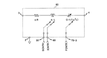
- the “two-terminal impedance z0” in this case can be expressed by using a series circuit of a resistance element, an inductive element, and a capacitive element as shown in FIG.
- the equivalent circuit 80 includes a first terminal 3, a second terminal 4, and a reference terminal 2, and further includes a sign switching input terminal 50 for inputting a sign switching control signal SCNTR, and an immittance level control signal ICNTR.
- An immittance level control input terminal 60 for inputting and a frequency control input terminal T9-3 for inputting a frequency control signal FCNTR are provided.
- the sign switching control signal SCNTR at least the signs of both the inductive element and the capacitive element can be simultaneously switched to positive / negative inversion.
- the element value of the inductive element and the element value of the capacitive element can be changed simultaneously according to the immittance level control signal ICNTR. At that time, the resonance frequency ⁇ is maintained constant between the two element values.
- FIG. 7 shows a case where the element value of the inductive element and the resonance frequency ⁇ are used as the two independent control amounts.
- the resonance frequency ⁇ is variable according to the frequency control signal FCNTR.
- both the sign and absolute value of the element value ⁇ R of the resistance element are variable.
- Table 2 also lists examples of effects in the second embodiment, but they are not used for explanation here.
- the value of the two-terminal impedance z0 at least one of the element value of the impedance control element RIL, the absolute value of the total gain ⁇ ta including the gain of the base circuit, or the sign thereof is determined according to the external signal. By changing, a wide range of characteristics and scaling are possible.
- the “desired two-terminal impedance z 0 ” constitutes a so-called “pseudo-short circuit” exhibiting “0 (zero)”.
- This circuit form is characterized by the qualitative relationship between the two-terminal immittance exhibited by the respective circuits as compared with the case where the impedance conversion generation circuit 5a is used as the immittance conversion generation circuit 5 described above.
- the relationship is a reciprocal relationship with each other.
- the admittance conversion generation circuit 5b shown in FIG. 8 when used as the immittance conversion generation circuit 5 in FIG. 2, the immittance formation circuit 1 shown in FIG. 2 operates as the bidirectional floating admittance conversion circuit 1.
- the admittance conversion generation circuit 5b includes an eleventh terminal T5-11, a twelfth terminal T5-12, a thirteenth terminal T5-13 (also referred to as a first feedback signal input terminal), a fourteenth terminal T5-14, A twenty-first terminal T5-21, a twenty-second terminal T5-22, a twenty-third terminal T5-23 (also referred to as a second feedback signal input terminal), and a twenty-fourth terminal T5-24.
- the eleventh terminal T5-11 is connected to the base of the first transistor Q1 via the connection point T10 and the terminal T11.
- the collector of the first transistor Q1 is connected at the connector T12 to the other terminal of the eleventh immittance level setting impedance RIL11 that connects one terminal to the DC potential V11, and to the terminal T5-12 via the terminal T13. Is done.
- the thirteenth terminal T5-13 is connected to the base of the second transistor Q2 through the connection point T15.
- the collector of the second transistor Q2 is connected to the other terminal of the twelfth immittance level setting impedance RIL12 that connects one terminal to the DC potential V12.
- the emitter of the first transistor Q1, the emitter of the second transistor Q2, and one terminal of the emitter common impedance RE are connected to each other at a connection point T16.
- the 21st terminal T5-21 is connected to the base of the third transistor Q3 via the connection point T20 and the terminal T21.
- the collector of the third transistor Q3 is connected to the other terminal of the 21st immittance level setting impedance RIL21 connecting one terminal to the DC potential V21 at the connection point T22, and to the 22nd terminal T5-22 via the terminal T23.
- the 23rd terminal T5-23 is connected to the base of the fourth transistor Q4 via the terminal T25.
- the collector of the fourth transistor Q4 is connected to the other terminal of the 22nd immittance level setting impedance RIL22 that connects one terminal to the DC potential V22.
- the emitter of the third transistor Q3, the emitter of the fourth transistor Q4, and the other terminal of the emitter common impedance RE are connected to each other at a connection point T26.
- the 14th terminal T5-14 is connected to the connection point T10, and the 24th terminal T5-24 is connected to the connection point T20.
- the type of admittance as two-terminal immittance that can be realized in the second embodiment is that the equivalent circuit corresponds to a parallel resonant circuit.
- Table 2 a part of an implementation example of “2-terminal admittance y0” is listed.
- the operation of the second embodiment will be described with reference to FIG.
- the admittance conversion generation circuit 5b shown in FIG. 8 is used as the immittance conversion generation circuit 5 of FIG. 2 constitutes a series addition type feedback circuit. That is, in the emitter common impedance RE between the terminal T16 and the terminal T26 in FIG.
- the signal applied to the eleventh terminal T5-11 and the signal applied to the terminal T5-13 are “voltage”. Acts as added or subtracted. Similarly, the signal applied to the 21st terminal T5-21 and the signal applied to the terminal T5-23 are operated so as to be added or subtracted as “voltage”.
- the horizontal and vertical axes in FIG. 9 are the same as those in FIG. From FIG. 9, the impedance developed between the first terminal 3 and the second terminal 4 is proportional to the resistance value of the resistor connected between the respective collectors of the four transistors and the DC power supply, and the cause It can be seen that it is proportional to the total gain including the gain of the circuit.
- the operation of the floating immittance formation circuit 1 when the admittance conversion generation circuit 5b is used will be described using mathematical expressions.
- the input impedance Zin between the first terminal 3 and the second terminal 4 of the floating immittance conversion circuit 1 (the reciprocal of the input admittance y0) can be approximated by the following equation.
- R IL11 , R IL12 , R IL21 , and R IL22 are resistors arranged between the respective collector terminals of the four transistors Q1, Q2, Q3, and Q4 and the DC power supply. , Everything is equally as R IL .
- ⁇ is the current amplification factor of the four transistors Q1, Q2, Q3, and Q4, and is assumed to be equal.
- ⁇ ta is a total gain including a gain from the twelfth terminal T5-12 to the thirteenth terminal T5-13, and a total gain including a gain from the twenty-second terminal T5-22 to the twenty-third terminal T5-23. Since they can be easily set equal, they are assumed to be equal. This value is generally a complex quantity.
- the positive and negative signs correspond to a negative feedback operation and a positive feedback operation.
- the term “floating property” is combined with the term “floating property” in addition to the so-called “floating property” and the performance of “separation” between the performance expression terminal and the performance control terminal.
- This isolation is governed, for example, by the isolation between the base and collector of the transistors Q1 and Q2 in FIG.
- cascode connection is one method.
- the base circuit 9 may be any circuit such as a unidirectional three-terminal circuit, a bidirectional three-terminal circuit, and a two-terminal circuit. Moreover, it is not always necessary to include an amplification effect. Further, an imaginary resonance circuit combining “ ⁇ L” and “+ C” is also possible as an element that governs the frequency characteristics of the base circuit.
Landscapes
- Amplifiers (AREA)
- Networks Using Active Elements (AREA)
Abstract
L'invention concerne un circuit de formation d'immitance flottante qui ne subit pas l'influence de variations du potentiel de référence, en d'autre termes, qui peut produire une immitance à deux bornes dans des conditions de flottement par rapport à un potentiel de référence. L'invention concerne également un circuit d'immitance flottante mettant en oeuvre ce circuit de formation d'immitance flottante. Plus spécifiquement, l'invention concerne un circuit de formation d'immitance flottante qui comporte: une paire de bornes de connexion aval et amont; au moins deux bornes de connexion d'un circuit d'origine; un circuit détecteur de tension différentielle amenant à l'une des bornes de connexion d'un circuit d'origine un signal de différence de potentiel électrique représentant la différence de potentiel électrique côté entrée, différence qui apparaît à chacune des bornes de connexion aval et amont; un circuit d'alimentation de courant qui admet un courant amont provenant de la borne de connexion amont, lequel courant correspond à une différence de potentiel électrique côté sortie entre un potentiel électrique d'origine au niveau de l'autre borne de connexion du circuit d'origine et un potentiel électrique standard d'une borne de connexion standard, et qui amène à la borne de connexion aval un courant aval égal au courant amont.
Priority Applications (4)
| Application Number | Priority Date | Filing Date | Title |
|---|---|---|---|
| PCT/JP2013/052896 WO2014122753A1 (fr) | 2013-02-07 | 2013-02-07 | Circuit de formation d'immitance flottante et circuit d'immitance flottante mettant en oeuvre celui-ci |
| PCT/JP2013/067316 WO2014122808A1 (fr) | 2013-02-07 | 2013-06-25 | Circuit de conversion d'immitance et filtre associé |
| JP2014560629A JP6041907B2 (ja) | 2013-02-07 | 2013-06-25 | イミタンス変換回路及びフィルタ |
| US14/766,582 US9401695B2 (en) | 2013-02-07 | 2013-06-25 | Immittance conversion circuit and filter |
Applications Claiming Priority (1)
| Application Number | Priority Date | Filing Date | Title |
|---|---|---|---|
| PCT/JP2013/052896 WO2014122753A1 (fr) | 2013-02-07 | 2013-02-07 | Circuit de formation d'immitance flottante et circuit d'immitance flottante mettant en oeuvre celui-ci |
Publications (1)
| Publication Number | Publication Date |
|---|---|
| WO2014122753A1 true WO2014122753A1 (fr) | 2014-08-14 |
Family
ID=51299366
Family Applications (2)
| Application Number | Title | Priority Date | Filing Date |
|---|---|---|---|
| PCT/JP2013/052896 Ceased WO2014122753A1 (fr) | 2013-02-07 | 2013-02-07 | Circuit de formation d'immitance flottante et circuit d'immitance flottante mettant en oeuvre celui-ci |
| PCT/JP2013/067316 Ceased WO2014122808A1 (fr) | 2013-02-07 | 2013-06-25 | Circuit de conversion d'immitance et filtre associé |
Family Applications After (1)
| Application Number | Title | Priority Date | Filing Date |
|---|---|---|---|
| PCT/JP2013/067316 Ceased WO2014122808A1 (fr) | 2013-02-07 | 2013-06-25 | Circuit de conversion d'immitance et filtre associé |
Country Status (3)
| Country | Link |
|---|---|
| US (1) | US9401695B2 (fr) |
| JP (1) | JP6041907B2 (fr) |
| WO (2) | WO2014122753A1 (fr) |
Families Citing this family (3)
| Publication number | Priority date | Publication date | Assignee | Title |
|---|---|---|---|---|
| FR3037745B1 (fr) * | 2015-06-22 | 2020-11-20 | Tekcem | Procede et appareil pour accord automatique d'une matrice impedance, et emetteur radio utilisant cet appareil |
| US9548721B1 (en) * | 2015-11-24 | 2017-01-17 | King Fahd University Of Petroleum And Minerals | Floating immittance emulator |
| CN111769829B (zh) * | 2020-07-22 | 2023-12-08 | 上海先积集成电路有限公司 | 一种支持正反接的信号转换电路 |
Citations (3)
| Publication number | Priority date | Publication date | Assignee | Title |
|---|---|---|---|---|
| JPH06141354A (ja) * | 1992-10-22 | 1994-05-20 | Hitachi Ltd | 加入者回路 |
| JP2003133907A (ja) * | 2001-10-24 | 2003-05-09 | Rohm Co Ltd | 等価インダクタ回路 |
| JP2005328272A (ja) * | 2004-05-13 | 2005-11-24 | Nec Electronics Corp | Pll回路およびそれを用いた周波数設定回路 |
Family Cites Families (4)
| Publication number | Priority date | Publication date | Assignee | Title |
|---|---|---|---|---|
| WO1997032396A1 (fr) * | 1996-03-01 | 1997-09-04 | Matsushita Electric Industrial Co., Ltd. | Resistance dependant de la frequence |
| US6121940A (en) | 1997-09-04 | 2000-09-19 | Ail Systems, Inc. | Apparatus and method for broadband matching of electrically small antennas |
| JP4720308B2 (ja) * | 2005-06-15 | 2011-07-13 | ソニー株式会社 | インピーダンス変換回路 |
| KR20120123081A (ko) | 2010-02-09 | 2012-11-07 | 마크디바이시스 가부시키가이샤 | 반공진 주파수 가변형 복합 공진 회로 |
-
2013
- 2013-02-07 WO PCT/JP2013/052896 patent/WO2014122753A1/fr not_active Ceased
- 2013-06-25 JP JP2014560629A patent/JP6041907B2/ja not_active Expired - Fee Related
- 2013-06-25 US US14/766,582 patent/US9401695B2/en not_active Expired - Fee Related
- 2013-06-25 WO PCT/JP2013/067316 patent/WO2014122808A1/fr not_active Ceased
Patent Citations (3)
| Publication number | Priority date | Publication date | Assignee | Title |
|---|---|---|---|---|
| JPH06141354A (ja) * | 1992-10-22 | 1994-05-20 | Hitachi Ltd | 加入者回路 |
| JP2003133907A (ja) * | 2001-10-24 | 2003-05-09 | Rohm Co Ltd | 等価インダクタ回路 |
| JP2005328272A (ja) * | 2004-05-13 | 2005-11-24 | Nec Electronics Corp | Pll回路およびそれを用いた周波数設定回路 |
Also Published As
| Publication number | Publication date |
|---|---|
| JPWO2014122808A1 (ja) | 2017-01-26 |
| JP6041907B2 (ja) | 2016-12-14 |
| US20150381145A1 (en) | 2015-12-31 |
| WO2014122808A1 (fr) | 2014-08-14 |
| US9401695B2 (en) | 2016-07-26 |
Similar Documents
| Publication | Publication Date | Title |
|---|---|---|
| Yuce et al. | A modified CFOA and its applications to simulated inductors, capacitance multipliers, and analog filters | |
| Yuce et al. | New CFOA-based first-order all-pass filters and their applications | |
| CN107104655B (zh) | 具有射极跟随器晶体管和伺服环路的滤波器电路 | |
| Abaci et al. | A new DVCC+ based second-order current-mode universal filter consisting of only grounded capacitors | |
| Dogan et al. | Supplementary single active device based grounded immittance function simulators | |
| Channumsin et al. | Single-input four-output voltage-mode universal filter using single DDCCTA | |
| WO2014122753A1 (fr) | Circuit de formation d'immitance flottante et circuit d'immitance flottante mettant en oeuvre celui-ci | |
| Pal et al. | Single CDBA based current mode first order multifunction filter | |
| Yuce et al. | Universal resistorless current‐mode filters employing CCCIIs | |
| US8368461B2 (en) | Second-order low-pass filter | |
| CN110212876A (zh) | 带内置负反馈的跟随器电路结构 | |
| Abaci et al. | Second-order voltage-mode universal filters using two DVCCs, two grounded capacitors and four resistors | |
| US11528011B2 (en) | Method for tunably multiplying an impedance | |
| EP1977507A1 (fr) | Amplificateur à entrées multiples et sorties multiples | |
| US9013237B1 (en) | Distributed transconductance amplifier | |
| Kamath | Novel DO-OTA based current-mode grounded capacitor multiplier | |
| Chaichana et al. | Current-mode MISO filter using CCCDTAs and grounded capacitors | |
| Alpaslan et al. | New grounded inductor simulator using unity gain cells | |
| JPWO1997032396A1 (ja) | 周波数依存抵抗器 | |
| JP6470213B2 (ja) | 可変利得増幅器 | |
| Yuce et al. | Signal limitations of the current-mode filters employing current conveyors | |
| Sagbas et al. | Realization of a general resistorless active biquad using CBTA | |
| Kamat | Novel large value grounded capacitor realizations using OTAs and small capacitors | |
| Agarwal et al. | Compact Design of Universal biquadratic filter using Basic Current Conveyor and Transconductance Amplifier | |
| bin Md Idros | A design of butterworth low pass filter's layout basideal filter approximation on the ideal filter approximation |
Legal Events
| Date | Code | Title | Description |
|---|---|---|---|
| 121 | Ep: the epo has been informed by wipo that ep was designated in this application |
Ref document number: 13874263 Country of ref document: EP Kind code of ref document: A1 |
|
| NENP | Non-entry into the national phase |
Ref country code: DE |
|
| NENP | Non-entry into the national phase |
Ref country code: JP |
|
| 32PN | Ep: public notification in the ep bulletin as address of the adressee cannot be established |
Free format text: NOTING OF LOSS OF RIGHTS PURSUANT TO RULE 112(1) EPC (EPO FORM 1205 DATED 25/01/2016) |
|
| 122 | Ep: pct application non-entry in european phase |
Ref document number: 13874263 Country of ref document: EP Kind code of ref document: A1 |