WO2014122910A1 - Dispositif mems - Google Patents
Dispositif mems Download PDFInfo
- Publication number
- WO2014122910A1 WO2014122910A1 PCT/JP2014/000547 JP2014000547W WO2014122910A1 WO 2014122910 A1 WO2014122910 A1 WO 2014122910A1 JP 2014000547 W JP2014000547 W JP 2014000547W WO 2014122910 A1 WO2014122910 A1 WO 2014122910A1
- Authority
- WO
- WIPO (PCT)
- Prior art keywords
- electrode
- mems device
- substrate
- movable portion
- fixed electrode
- Prior art date
- Legal status (The legal status is an assumption and is not a legal conclusion. Google has not performed a legal analysis and makes no representation as to the accuracy of the status listed.)
- Ceased
Links
Images











Classifications
-
- B—PERFORMING OPERATIONS; TRANSPORTING
- B81—MICROSTRUCTURAL TECHNOLOGY
- B81B—MICROSTRUCTURAL DEVICES OR SYSTEMS, e.g. MICROMECHANICAL DEVICES
- B81B3/00—Devices comprising flexible or deformable elements, e.g. comprising elastic tongues or membranes
- B81B3/0002—Arrangements for avoiding sticking of the flexible or moving parts
- B81B3/0008—Structures for avoiding electrostatic attraction, e.g. avoiding charge accumulation
-
- G—PHYSICS
- G01—MEASURING; TESTING
- G01P—MEASURING LINEAR OR ANGULAR SPEED, ACCELERATION, DECELERATION, OR SHOCK; INDICATING PRESENCE, ABSENCE, OR DIRECTION, OF MOVEMENT
- G01P15/00—Measuring acceleration; Measuring deceleration; Measuring shock, i.e. sudden change of acceleration
- G01P15/02—Measuring acceleration; Measuring deceleration; Measuring shock, i.e. sudden change of acceleration by making use of inertia forces using solid seismic masses
- G01P15/08—Measuring acceleration; Measuring deceleration; Measuring shock, i.e. sudden change of acceleration by making use of inertia forces using solid seismic masses with conversion into electric or magnetic values
- G01P15/125—Measuring acceleration; Measuring deceleration; Measuring shock, i.e. sudden change of acceleration by making use of inertia forces using solid seismic masses with conversion into electric or magnetic values by capacitive pick-up
-
- B—PERFORMING OPERATIONS; TRANSPORTING
- B81—MICROSTRUCTURAL TECHNOLOGY
- B81B—MICROSTRUCTURAL DEVICES OR SYSTEMS, e.g. MICROMECHANICAL DEVICES
- B81B2201/00—Specific applications of microelectromechanical systems
- B81B2201/02—Sensors
- B81B2201/0228—Inertial sensors
- B81B2201/0235—Accelerometers
-
- G—PHYSICS
- G01—MEASURING; TESTING
- G01P—MEASURING LINEAR OR ANGULAR SPEED, ACCELERATION, DECELERATION, OR SHOCK; INDICATING PRESENCE, ABSENCE, OR DIRECTION, OF MOVEMENT
- G01P15/00—Measuring acceleration; Measuring deceleration; Measuring shock, i.e. sudden change of acceleration
- G01P15/02—Measuring acceleration; Measuring deceleration; Measuring shock, i.e. sudden change of acceleration by making use of inertia forces using solid seismic masses
- G01P15/08—Measuring acceleration; Measuring deceleration; Measuring shock, i.e. sudden change of acceleration by making use of inertia forces using solid seismic masses with conversion into electric or magnetic values
- G01P2015/0805—Measuring acceleration; Measuring deceleration; Measuring shock, i.e. sudden change of acceleration by making use of inertia forces using solid seismic masses with conversion into electric or magnetic values being provided with a particular type of spring-mass-system for defining the displacement of a seismic mass due to an external acceleration
- G01P2015/0822—Measuring acceleration; Measuring deceleration; Measuring shock, i.e. sudden change of acceleration by making use of inertia forces using solid seismic masses with conversion into electric or magnetic values being provided with a particular type of spring-mass-system for defining the displacement of a seismic mass due to an external acceleration for defining out-of-plane movement of the mass
- G01P2015/0825—Measuring acceleration; Measuring deceleration; Measuring shock, i.e. sudden change of acceleration by making use of inertia forces using solid seismic masses with conversion into electric or magnetic values being provided with a particular type of spring-mass-system for defining the displacement of a seismic mass due to an external acceleration for defining out-of-plane movement of the mass for one single degree of freedom of movement of the mass
- G01P2015/0834—Measuring acceleration; Measuring deceleration; Measuring shock, i.e. sudden change of acceleration by making use of inertia forces using solid seismic masses with conversion into electric or magnetic values being provided with a particular type of spring-mass-system for defining the displacement of a seismic mass due to an external acceleration for defining out-of-plane movement of the mass for one single degree of freedom of movement of the mass the mass constituting a pendulum having the pivot axis disposed symmetrically between the longitudinal ends, the center of mass being shifted away from the plane of the pendulum which includes the pivot axis
-
- H—ELECTRICITY
- H10—SEMICONDUCTOR DEVICES; ELECTRIC SOLID-STATE DEVICES NOT OTHERWISE PROVIDED FOR
- H10D—INORGANIC ELECTRIC SEMICONDUCTOR DEVICES
- H10D48/00—Individual devices not covered by groups H10D1/00 - H10D44/00
- H10D48/50—Devices controlled by mechanical forces, e.g. pressure
Definitions
- the present technical field relates to MEMS (Micro-Electro-Mechanical Systems) devices.
- FIG. 7 is a perspective view showing the internal structure of a package 1300 incorporating a conventional MEMS device.
- FIG. 7 shows a state in which the lid of the package 1300 is opened.
- the package 1300 is mounted on the substrate 1500.
- a sensor chip 1100 and an integrated circuit 1200 such as an application specific integrated circuit (ASIC) are mounted on the package 1300.
- the MEMS device is housed in the sensor chip 1100.
- the integrated circuit 1200 performs various operations based on the output from the sensor chip 1100.
- a terminal 1400 is drawn from the package 1300 and connected to the substrate 1500.
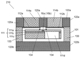
- FIG. 8A is a vertical sectional view of a conventional acceleration sensor 210.
- FIG. 8B is a horizontal sectional schematic view of a conventional acceleration sensor 210.
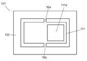
- FIG. 8C is a top view of the movable body 101 of the conventional acceleration sensor 210.
- FIG. 8D is a bottom view of the movable body 101 of the conventional acceleration sensor 210.
- the capacitive acceleration sensor 210 includes the movable body 101 and the electrode substrates 122a and 122b.
- the movable body 101 includes a movable portion 111, a frame 133, and beams 16a and 16b.
- the frame 133 is an outer frame surrounding the movable portion 111.
- the movable portion 111 is supported by the frame 133 with the beams 16a and 16b as pivot axes.
- extension portions of the beams 16a and 16b are used as a shaft portion 145, and portions other than the shaft portion 145 of the movable portion 111 are used as a swinging portion 144a and a swinging portion 144b.
- the swinging portion 144a is a cube
- the swinging portion 144b is a cube having an opening 111d on the opposite side of the surface facing the fixed electrode 112b.
- the frame 133 is formed of silicon (Si).
- the movable portion 111 is formed of SOI (Silicon on Insulator). Specifically, the movable portion 111 is formed by the oxide film 111b such as SiO 2 being sandwiched between the Si layer 111a and the Si layer 111c.
- Electrode substrates 122 a and 122 b are provided on both sides of the movable body 101.
- the periphery of the movable body 101 and the periphery of the electrode substrates 122a and 122b are joined by anodic bonding.
- the electrode substrate 122a includes a substrate portion 120a, extraction electrodes 114a and 114b, and fixed electrodes 112a and 112b.
- the substrate portion 120a is formed of glass.
- the extraction electrodes 114a and 114b are formed of Si.
- the electrode substrate 122 b is configured of a substrate portion 120 b formed of glass.
- the fixed electrodes 112a and 112b are metal thin films formed by sputtering or the like.
- the fixed electrode 112a is formed in at least a part of a region facing the swinging portion 144a of the electrode substrate 122a.
- the fixed electrode 112b is formed in at least a part of a region facing the swinging portion 144b of the electrode substrate 122a.
- the extraction electrodes 114a and 114b are embedded in the substrate portion 120a, whereby the potentials of the fixed electrodes 112a and 112b can be extracted to the upper surface of the electrode substrate 122a.
- the capacitance between the fixed electrode 112 a and the movable portion 111 and the capacitance between the fixed electrode 112 b and the movable portion 111 change.
- the acceleration sensor 210 detects the displacement of the movable portion 111 from the change in electrostatic capacitance between the movable portion 111 and the fixed electrodes 112a and 112b, and detects the acceleration based on this displacement.
- a plurality of projecting stoppers 134 are formed on the surface of the movable portion 111 facing the fixed electrodes 112 a and 112 b. By forming the stopper 134, even when a large acceleration is applied to the movable portion 111, the movable portion 111 can be prevented from colliding against the fixed electrodes 112a and 112b and being damaged.
- the bonding portions of the electrode substrates 122a and 122b with the frame 133 are the substrate portions 120a and 120b, and are formed of glass. And the junction part with electrode substrate 122a, 122b of movable body 101 is formed with silicon (Si).
- Anodic bonding is used for bonding the electrode substrates 122 a and 122 b and the movable body 101. However, at the time of anodic bonding, depending on the applied voltage, an electrostatic attraction force is generated between the glass and Si. A part of the movable portion 111 may be attracted to the electrode substrate 122 a side by the electrostatic attraction force and may be bonded.
- FIG. 9A is a vertical sectional view of another conventional acceleration sensor 212.
- FIG. 9B is a horizontal sectional schematic view of another conventional acceleration sensor 212.
- a recess 130 is provided in a region (hereinafter, referred to as “facing region”) of the movable portion 111 facing a portion sandwiched by the fixed electrode 112 a and the fixed electrode 112 b.
- the recess 130 is formed by thinning at least a part of the facing region of the movable portion 111.
- the electrostatic attraction can be reduced. By making the electrostatic attraction force smaller than the elastic force, it is possible to suppress the movable portion 111 from being bonded to the substrate portion 120a.
- the beams 16a, 16b need to be very thin. As a result, the beams 16a and 16b may be deformed by electrostatic attraction generated at the time of anodic bonding, and the beams 16a and 16b may be bonded to the glass.
- the beams 16a and 16b are made extremely thin, when the movable body 101 and the electrode substrate 122a are anodically bonded at a voltage of about 400 V, the beams 16a and 16b are attracted to the substrate portion 120a by electrostatic attraction generated at the time of anodic bonding. Therefore, the beams 16a and 16b may be deformed, and the beams 16a and 16b may be bonded to the substrate portion 120a.
- the MEMS device comprises a movable portion, a frame, a beam, and an electrode substrate.
- the frame is separated from the movable part and surrounds the periphery of the movable part.
- the beam extends from at least a portion of the frame and is connected to the moveable portion.
- the electrode substrate has a fixed electrode, an extension electrode, and a substrate portion.
- the electrode substrate faces the movable portion, and the periphery is bonded to the periphery of the frame.
- the extension portion of the beam is a shaft portion, and the portion other than the shaft portion of the movable portion is a swing portion.
- the fixed electrode is formed on at least a part of the area of the electrode substrate facing the swinging portion.
- the extended electrode is connected to the fixed electrode, and is formed in at least a part of the region of the electrode substrate facing the shaft.
- FIG. 1 is a perspective view showing the internal structure of a package incorporating the MEMS device in the present embodiment.
- FIG. 2A is a vertical sectional view of the acceleration sensor according to the present embodiment.
- FIG. 2B is a horizontal cross-sectional schematic view of the acceleration sensor in the present embodiment.
- FIG. 2C is a top view of the movable body of the acceleration sensor according to the present embodiment.
- FIG. 2D is a bottom view of the movable body of the acceleration sensor according to the present embodiment.
- FIG. 2E is a schematic view illustrating the recess of the acceleration sensor according to the present embodiment.
- FIG. 2F is a schematic view illustrating a dummy electrode of another acceleration sensor according to the present embodiment.
- FIG. 3A is a vertical cross-sectional view of still another acceleration sensor in the present embodiment.
- FIG. 3B is a horizontal cross-sectional schematic view of still another acceleration sensor in the present embodiment.
- FIG. 4A is a vertical cross-sectional view of still another acceleration sensor in the present embodiment.
- FIG. 4B is a horizontal cross-sectional schematic view of still another acceleration sensor according to the present embodiment.
- FIG. 4C is a schematic bottom view of the fixed electrode and the extended electrode of still another acceleration sensor according to the present embodiment.
- FIG. 4D is a horizontal cross-sectional schematic view of still another acceleration sensor in the present embodiment.
- FIG. 4E is a schematic bottom view of the fixed electrode and the extended electrode of still another acceleration sensor according to the present embodiment.
- FIG. 4F is a schematic bottom view of the fixed electrode and the extended electrode of still another acceleration sensor according to the present embodiment.
- FIG. 5A is a schematic view illustrating the configuration of a movable portion and a fixed electrode of a conventional acceleration sensor.
- FIG. 5B is a schematic view illustrating the configuration of the movable portion, the fixed electrode, and the dummy electrode of the acceleration sensor according to the present embodiment.
- FIG. 5C is a schematic view illustrating the configuration of the movable portion, the fixed electrode, and the extension electrode of another acceleration sensor according to the present embodiment.
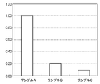
- FIG. 6 is a graph showing the maximum deflection of the beam portion of the acceleration sensor.
- FIG. 7 is a perspective view showing the internal structure of a package incorporating a conventional MEMS device.
- FIG. 8A is a vertical cross-sectional view of a conventional acceleration sensor.
- FIG. 8B is a schematic horizontal cross-sectional view of a conventional acceleration sensor.
- FIG. 8C is a top view of a movable body of a conventional acceleration sensor.
- FIG. 8D is a bottom view of the movable body of the conventional acceleration sensor.
- FIG. 9A is a vertical sectional view of another conventional acceleration sensor.
- FIG. 9B is a horizontal cross-sectional schematic view of another conventional acceleration sensor.
- FIG. 1 is a perspective view showing the internal structure of a package incorporating the MEMS device in the present embodiment.
- FIG. 1 shows a state in which the lid of the package 300 is opened.
- the package 300 is mounted on the substrate 500.
- the sensor chip 100 and an integrated circuit 200 such as an application specific integrated circuit (ASIC) are mounted.
- the MEMS device is housed in the sensor chip 100.
- the integrated circuit 200 performs various operations based on the output from the sensor chip 100.
- the terminal 400 is pulled out of the package 300 and connected to the substrate 500.
- a capacitive acceleration sensor which is a MEMS device, will be described.
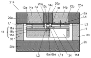
- FIG. 2A is a vertical cross-sectional view of acceleration sensor 214 in the present embodiment.
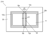
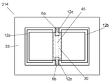
- FIG. 2B is a horizontal cross-sectional schematic view of the acceleration sensor 214 in the present embodiment.
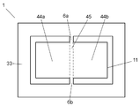
- FIG. 2C is a top view of the movable body 1 of the acceleration sensor 214 in the present embodiment.
- FIG. 2D is a bottom view of the movable body 1 of the acceleration sensor 214 in the present embodiment.
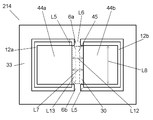
- FIG. 2E is a schematic view illustrating the recess 30 of the acceleration sensor 214 according to the present embodiment. In the schematic diagram, a hidden portion is indicated by a solid line for the purpose of explanation.
- the MEMS device includes the movable body 1 and the electrode substrates 2a and 2b.
- the movable body 1 has a movable portion 11, a frame 33, and beams 6a and 6b.
- the frame 33 is separated from the movable portion 11 and surrounds the periphery of the movable portion 11.
- the beams 6 a and 6 b extend from two points of the frame 33 and are connected to the movable portion 11.
- the frame 33 and the beams 6a and 6b are formed of silicon (Si).
- the movable portion 11 is formed of SOI (Silicon on Insulator). Specifically, the movable portion 11 is formed by sandwiching the oxide film 11 b between the Si layer 11 a (first Si layer) and the Si layer 11 c (second Si layer). Here, the oxide film 11 b is SiO 2 or SiO.
- the beams 6a and 6b are formed of the Si layer 11a (first Si layer).
- the frame 33 is an outer frame surrounding the movable portion 11.
- the movable portion 11 is supported by the frame 33 with the beams 6a and 6b as pivot axes.
- the extension portions of the beams 6a and 6b are the shaft portion 45, and portions other than the shaft portion 45 of the movable portion 11 are the rocking portion 44a (first rocking portion)
- the moving part 44 b (second swinging part) is used.
- the swinging portion 44a is a cube
- the swinging portion 44b is a cube having an opening 11d on the opposite side of the surface facing the fixed electrode 12b.
- the fixed electrodes 12a and 12b are metal thin films such as an Al-Si film or an Al-Ti film, and are formed by sputtering or the like.
- the fixed electrode 12a (first fixed electrode) is formed on at least a part of a region of the electrode substrate 2a facing the swinging portion 44a.
- the fixed electrode 12 b (second fixed electrode) is formed in at least a part of the region of the electrode substrate 2 a facing the swinging portion 44 b.
- the lead-out electrodes 14a and 14b are embedded in the substrate portion 20a, whereby the potential of the fixed electrodes 12a and 12b can be drawn to the upper surface of the electrode substrate 2a.
- the dummy electrode 12 c is formed in at least a part of the region of the electrode substrate 2 a facing the shaft 45.
- the extraction electrode 14c is embedded in the substrate portion 20a, whereby the potential of the dummy electrode 12c can be extracted to the upper surface of the electrode substrate 2a.
- the capacitance between the fixed electrode 12a and the swinging portion 44a and the capacitance between the fixed electrode 12b and the swinging portion 44b change.
- the acceleration sensor 214 detects the displacement of the movable portion 11 from the change in electrostatic capacitance between the movable portion 11 and the fixed electrodes 12a and 12b, and detects the acceleration based on the displacement.
- a plurality of projecting stoppers 34 are formed on the surface of the movable portion 11 facing the fixed electrodes 12 a and 12 b. By forming the stopper 34, even when a large acceleration is applied to the movable portion 11, the movable portion 11 can be prevented from colliding against the fixed electrodes 12a and 12b and being damaged.
- the bonding portions of the electrode substrates 2a and 2b with the frame 33 are the substrate portions 20a and 20b, and are formed of glass. And the junction part with electrode substrate 2a, 2b of frame 33 is formed with silicon (Si). Anodic bonding is used to bond the electrode substrates 2 a and 2 b to the movable body 1.
- a recess 30 is provided in a region (hereinafter, referred to as “opposing region”) of the movable portion 11 facing a portion sandwiched between the fixed electrode 12 a and the fixed electrode 12 b.
- the recess 30 is formed by thinning at least a part of the facing region of the movable portion 11.
- the distance L12 in the lateral direction of the recess 30 is 40 ⁇ m
- the distance L13 in the longitudinal direction of the recess 30 is 800 ⁇ m
- the depth L11 of the recess 30 is 11 ⁇ m.
- the distance in the vertical direction of the facing region is 1000 ⁇ m
- the distance L7 in the horizontal direction is 40 ⁇ m. That is, the recess 30 is formed by removing the area of 800 ⁇ 40 ⁇ m 2 by etching to a depth of 11 ⁇ m in the opposing area of the area 1000 ⁇ 40 ⁇ m 2 .
- the distance L7 between the fixed electrodes 12a and 12b is 40 ⁇ m
- the width L8 of the movable portion 11 is 1000 ⁇ m
- the distance L3 between the substrate portion 20a and the movable portion 11 is 2.2 ⁇ m
- the thickness of the fixed electrodes 12a and 12b Let L4 be 0.2 ⁇ m.
- an electrostatic attraction force of about 16 mN is generated in the movable portion 11.
- the beams 6a and 6b have a width L6 of 12 ⁇ m, a thickness L2 of 11 ⁇ m, a length L5 of 150 ⁇ m, and a height L1 of the stopper 34 formed on the movable portion 11 of 1.1 ⁇ m.
- the elastic force when the movable portion 11 is attracted by 0.9 ⁇ m is 3.6 mN.
- the electrostatic attraction force exceeds the elastic force, the movable portion 11 may be bonded to the substrate portion 20a.
- the electrostatic attraction can be reduced to 3.5 mN. That is, by making the electrostatic attraction force smaller than the elastic force, it is possible to suppress that the movable portion 11 is bonded to the substrate portion 20a.
- the electrode substrate 2a has a dummy electrode 12c in a region facing the shaft 45.
- the dummy electrode 12c is electrically floating.
- the dummy electrode 12 c is a metal thin film such as an Al—Si film or an Al—Ti film, and can be formed by the same process as the fixed electrodes 12 a and 12 b.
- the dummy electrode 12c is connected to one end of the lead electrode 14c.
- the width L21 of the dummy electrode 12c is preferably slightly larger than the width L6 of the beams 6a and 6b.
- the width L21 of the dummy electrode 12c is preferably 20 ⁇ m or more. Such a configuration can further reduce the electrostatic attraction generated at the time of anodic bonding.
- the dummy electrode 12c is formed along the region facing the recess 30, but the present embodiment is not limited to this. As shown in FIG. 2F, the dummy electrode 12c may be formed in at least a part of the region of the electrode substrate 2a facing the shaft 45.
- the concave portion 30 is formed, 3.5 mN of electrostatic attraction force is generated in the movable portion 11 when anodic bonding is performed. Therefore, it is desirable to form the dummy electrode 12 c not only in the area facing the shaft 45 but also in the area facing the recess 30.
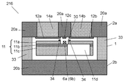
- FIG. 3A is a vertical cross-sectional view of acceleration sensor 216 in the present embodiment.
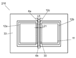
- FIG. 3B is a horizontal cross-sectional schematic view of the acceleration sensor 216 in the present embodiment.
- the acceleration sensor 216 differs from the acceleration sensor 214 in that the lead-out electrode 14c is not formed, and the dummy electrode 12c is connected to the common potential.
- a hidden portion is indicated by a solid line for the purpose of explanation.
- the dummy electrode 12c is connected to the frame 33 formed of Si. That is, the dummy electrode 12c and the movable portion 11 are at the same potential.
- the beams 6a and 6b do not easily come in contact with the electrode substrate 2a. That is, by connecting the dummy electrode 12c to the common potential, the electrostatic attraction force generated at the time of anodic bonding can be further reduced, so that the acceleration sensor 216 resistant to disturbance can be obtained.
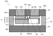
- FIG. 4A is a vertical sectional view of acceleration sensor 218 in the present embodiment.
- FIG. 4B is a horizontal cross-sectional schematic view of the acceleration sensor 218 in the present embodiment.
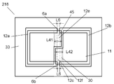
- FIG. 4C is a schematic bottom view of the fixed electrodes 12a and 12b and the extended electrodes 12e and 12f of the acceleration sensor 218 in the present embodiment.
- the acceleration sensor 218 differs from the acceleration sensor 214 in that the dummy electrode 12 c and the lead-out electrode 14 c are not formed, and at least one of the fixed electrode 12 a and the fixed electrode 12 b extends to a region facing the shaft 45 That is the point.
- a hidden portion is indicated by a solid line for the purpose of explanation.
- an electrode is formed in the region facing the shaft 45 of the electrode substrate 2a by extending a part of the fixed electrode 12a (first fixed electrode) toward the fixed electrode 12b.
- the extended rectangular electrode is referred to as an extended electrode 12e (first extended electrode).
- an electrode is formed also in a region facing the shaft 45 of the electrode substrate 2a.
- the extended rectangular electrode is referred to as an extended electrode 12 f (second extended electrode).
- the extended electrodes 12e and 12f can be integrally formed with the fixed electrodes 12a and 12b.
- the material of the extended electrodes 12e and 12f is a metal thin film such as an Al—Si film or an Al—Ti film.
- the width L41 of the extended electrode 12e and the width L42 of the extended electrode 12f are preferably 40 ⁇ m or more. This configuration makes it difficult to charge the upper portions of the beams 6a and 6b.
- FIG. 4B the extended electrode 12e is formed in most of the region facing the recess 30 of the electrode substrate 2a, but the present embodiment is not limited to this.
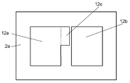
- FIG. 4D is a horizontal cross-sectional schematic view of the acceleration sensor 219 in the present embodiment.
- the hidden portion is indicated by a solid line for the purpose of explanation.
- the expansion electrode 12e may be formed in at least a part of a region facing the shaft 45.
- the recess 30 may not be provided. However, the provision of the recess 30 can reduce the electrostatic attraction.
- the recessed portion 30 is provided, 3.5 mN of electrostatic attraction force is generated in the movable portion 11 when anodic bonding is performed, so that not only a part of the region facing the shaft portion 45 but also the recessed portion 30 is opposed. It is preferable to form the expansion electrodes 12e and 12f in most of the area to be formed.
- the extended electrode 12e and the extended electrode 12f are formed in point symmetry.
- the aspect of the extended electrodes 12e and 12f is not limited to this.
- the extended electrodes 12 e and 12f may be different.
- the extended electrodes 12 e and 12 f have a rectangular shape, but may have another shape such as a circular shape or a polygonal shape.
- the electrostatic attraction force generated at the time of anodic bonding is reduced, and the upper portions of beams 6a and 6b are hard to be charged. Therefore, even when an unnecessary signal is applied from the outside, beam 6a, 6b is difficult to contact with the electrode substrate 2a. Therefore, acceleration sensors 218, 219 resistant to disturbance can be obtained.
- the acceleration sensors 214 and 216 since the dummy electrodes 12c are provided separately from the fixed electrodes, the area of the fixed electrodes 12a and 12b is reduced by the area of the dummy electrodes 12c. Since the dummy electrode 12c does not contribute to the detection of the acceleration, the reduction of the area of the fixed electrodes 12a and 12b may result in a decrease in detection sensitivity. However, the acceleration sensors 218 and 219 do not have the dummy electrode 12 c. Therefore, the electrostatic attraction force generated at the time of anodic bonding can be reduced without reducing the detection sensitivity.
- the recess 30 is formed, but the recess 30 may not be formed. However, since the electrostatic attraction can be reduced by forming the recess 30, it is preferable to form the recess 30.
- the number of the beams 6a and 6b is not limited to two and may be one.
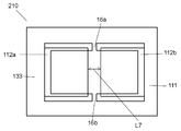
- FIG. 5A is a schematic view illustrating the configuration of the movable portion 111 and the fixed electrodes 112 a and 112 b of the conventional acceleration sensor 210.
- FIG. 5B is a schematic view illustrating the configuration of the movable portion 11, the fixed electrodes 12a and 12b, and the dummy electrode 12c of the acceleration sensor 214 in the present embodiment.
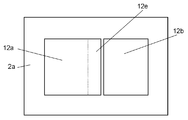
- FIG. 5C is a schematic view illustrating the configuration of the movable portion 11, the fixed electrodes 12a and 12b, and the extended electrodes 12e and 12f of the acceleration sensor 218 in the present embodiment.
- FIG. 5A shows a schematic view of the acceleration sensor 210 in the horizontal cross sectional direction.
- FIG. 5B shows a schematic view of the acceleration sensor 214 in the horizontal sectional direction.
- FIG. 5C shows a schematic view of the acceleration sensor 218 in the horizontal cross-sectional direction.
- the acceleration sensor 210 shown in FIG. 5A is a sample A
- the acceleration sensor 214 shown in FIG. 5B is a sample B
- the acceleration sensor 218 shown in FIG. 5C is a sample C.
- a hidden portion is indicated by a solid line for the purpose of explanation.
- the distance L7 between the fixed electrodes 112a and 112b is 40 ⁇ m.
- the width L21 of the dummy electrode 12c is 20 ⁇ m.
- the distance L63 from the fixed electrode 12a to the dummy electrode 12c is 20 ⁇ m, and the distance L64 from the fixed electrode 12b to the dummy electrode 12c is 20 ⁇ m.
- the widest distance L73 between the fixed electrodes 12a and 12b is 60 ⁇ m.
- the width L41 of the expansion electrode 12e and the width L42 of the expansion electrode 12f are 40 ⁇ m. That is, the narrowest distance L75 between the fixed electrodes 12a and 12b is 20 ⁇ m.
- the distance indicates the distance on the horizontal sectional view.
- FIG. 6 is a graph showing the maximum deflection of the beam portion of the acceleration sensor due to the electrostatic attraction generated at the time of anodic bonding.
- the maximum deflection amount of the beam 16a, 16b of the sample A is "1".
- the width L21 of the dummy electrode 12c is 20 ⁇ m
- the width from the fixed electrode 12a to the dummy electrode 12c is 20 ⁇ m
- the width from the fixed electrode 12b to the dummy electrode 12c is 20 ⁇ m. Is almost the same as the configuration of sample B. Therefore, the maximum deflection amount in that case is about 0.2.
- a fixed electrode (not shown) is further provided on the electrode substrate 12b, and an alternating voltage is applied between the movable portion 11 and the fixed electrode 12b to provide static electricity between the movable portion 11 and the fixed electrode 12b.
- the movable portion 11 may be vibrated in the vertical direction by applying an attractive force.
- the present embodiment is not limited to the above example, and various modifications are possible.
- the two fixed electrodes 12a and 12b are formed on the electrode substrate 2a, but the number of fixed electrodes is not limited to two.
- the shape, size, layout, etc. of the dummy electrode 12c can be appropriately changed.
- the MEMS device according to the present embodiment is useful as an electrostatic capacitance-type acceleration sensor because the beam is not easily bonded to glass when the movable body and the electrode substrate are anodically bonded.
Landscapes
- Engineering & Computer Science (AREA)
- Computer Hardware Design (AREA)
- Microelectronics & Electronic Packaging (AREA)
- Physics & Mathematics (AREA)
- General Physics & Mathematics (AREA)
- Pressure Sensors (AREA)
- Micromachines (AREA)
Abstract
Priority Applications (2)
| Application Number | Priority Date | Filing Date | Title |
|---|---|---|---|
| JP2014560677A JP6295435B2 (ja) | 2013-02-06 | 2014-02-03 | Memsデバイス |
| US14/764,572 US9550663B2 (en) | 2013-02-06 | 2014-02-03 | MEMS device |
Applications Claiming Priority (2)
| Application Number | Priority Date | Filing Date | Title |
|---|---|---|---|
| JP2013020990 | 2013-02-06 | ||
| JP2013-020990 | 2013-02-06 |
Publications (1)
| Publication Number | Publication Date |
|---|---|
| WO2014122910A1 true WO2014122910A1 (fr) | 2014-08-14 |
Family
ID=51299510
Family Applications (1)
| Application Number | Title | Priority Date | Filing Date |
|---|---|---|---|
| PCT/JP2014/000547 Ceased WO2014122910A1 (fr) | 2013-02-06 | 2014-02-03 | Dispositif mems |
Country Status (3)
| Country | Link |
|---|---|
| US (1) | US9550663B2 (fr) |
| JP (1) | JP6295435B2 (fr) |
| WO (1) | WO2014122910A1 (fr) |
Cited By (10)
| Publication number | Priority date | Publication date | Assignee | Title |
|---|---|---|---|---|
| JP2016045190A (ja) * | 2014-08-19 | 2016-04-04 | セイコーエプソン株式会社 | 物理量センサー、電子機器および移動体 |
| US9309106B2 (en) | 2013-07-08 | 2016-04-12 | Motion Engine Inc. | 3D MEMS device and method of manufacturing |
| WO2017150201A1 (fr) * | 2016-03-03 | 2017-09-08 | セイコーエプソン株式会社 | Dispositif de capteur, appareil électronique et corps mobile |
| US10214414B2 (en) | 2014-01-09 | 2019-02-26 | Motion Engine, Inc. | Integrated MEMS system |
| US10273147B2 (en) | 2013-07-08 | 2019-04-30 | Motion Engine Inc. | MEMS components and method of wafer-level manufacturing thereof |
| US10407299B2 (en) | 2015-01-15 | 2019-09-10 | Motion Engine Inc. | 3D MEMS device with hermetic cavity |
| US10768065B2 (en) | 2014-04-10 | 2020-09-08 | Mei Micro, Inc. | MEMS pressure sensor |
| US11287486B2 (en) | 2014-12-09 | 2022-03-29 | Motion Engine, Inc. | 3D MEMS magnetometer and associated methods |
| US11674803B2 (en) | 2014-06-02 | 2023-06-13 | Motion Engine, Inc. | Multi-mass MEMS motion sensor |
| US11852481B2 (en) | 2013-08-02 | 2023-12-26 | Motion Engine Inc. | MEMS motion sensor and method of manufacturing |
Families Citing this family (4)
| Publication number | Priority date | Publication date | Assignee | Title |
|---|---|---|---|---|
| US9810712B2 (en) | 2014-08-15 | 2017-11-07 | Seiko Epson Corporation | Physical quantity sensor, physical quantity sensor device, electronic equipment, and moving body |
| JP6464613B2 (ja) * | 2014-08-27 | 2019-02-06 | セイコーエプソン株式会社 | 物理量センサー、電子機器および移動体 |
| JP6847024B2 (ja) * | 2017-11-29 | 2021-03-24 | 株式会社日立製作所 | 加速度センサ |
| CN113955712B (zh) * | 2021-09-30 | 2026-03-20 | 瑞声开泰科技(武汉)有限公司 | 导电结构及其制备方法 |
Citations (5)
| Publication number | Priority date | Publication date | Assignee | Title |
|---|---|---|---|---|
| JP2005265565A (ja) * | 2004-03-18 | 2005-09-29 | Sony Corp | 容量検出型センサの製造方法および容量検出型センサ |
| JP2008070284A (ja) * | 2006-09-15 | 2008-03-27 | Ricoh Co Ltd | 半導体センサ及びその製造方法 |
| JP2010281789A (ja) * | 2009-06-08 | 2010-12-16 | Murata Mfg Co Ltd | 静電型デバイス |
| JP2011017693A (ja) * | 2009-06-09 | 2011-01-27 | Denso Corp | 半導体力学量センサの製造方法及び半導体力学量センサ |
| JP2011066429A (ja) * | 2010-09-30 | 2011-03-31 | Dainippon Printing Co Ltd | センサデバイス及びその製造方法 |
Family Cites Families (3)
| Publication number | Priority date | Publication date | Assignee | Title |
|---|---|---|---|---|
| JP4367189B2 (ja) * | 2004-03-19 | 2009-11-18 | いすゞ自動車株式会社 | 残留応力測定試験体および試験体の熱処理方法 |
| JP2012220376A (ja) | 2011-04-11 | 2012-11-12 | Panasonic Corp | 加速度センサ |
| TWI469254B (zh) * | 2011-12-29 | 2015-01-11 | Ind Tech Res Inst | 具多重電性通道的微機電裝置及其製作方法 |
-
2014
- 2014-02-03 JP JP2014560677A patent/JP6295435B2/ja not_active Expired - Fee Related
- 2014-02-03 US US14/764,572 patent/US9550663B2/en active Active
- 2014-02-03 WO PCT/JP2014/000547 patent/WO2014122910A1/fr not_active Ceased
Patent Citations (5)
| Publication number | Priority date | Publication date | Assignee | Title |
|---|---|---|---|---|
| JP2005265565A (ja) * | 2004-03-18 | 2005-09-29 | Sony Corp | 容量検出型センサの製造方法および容量検出型センサ |
| JP2008070284A (ja) * | 2006-09-15 | 2008-03-27 | Ricoh Co Ltd | 半導体センサ及びその製造方法 |
| JP2010281789A (ja) * | 2009-06-08 | 2010-12-16 | Murata Mfg Co Ltd | 静電型デバイス |
| JP2011017693A (ja) * | 2009-06-09 | 2011-01-27 | Denso Corp | 半導体力学量センサの製造方法及び半導体力学量センサ |
| JP2011066429A (ja) * | 2010-09-30 | 2011-03-31 | Dainippon Printing Co Ltd | センサデバイス及びその製造方法 |
Cited By (15)
| Publication number | Priority date | Publication date | Assignee | Title |
|---|---|---|---|---|
| US9309106B2 (en) | 2013-07-08 | 2016-04-12 | Motion Engine Inc. | 3D MEMS device and method of manufacturing |
| US10273147B2 (en) | 2013-07-08 | 2019-04-30 | Motion Engine Inc. | MEMS components and method of wafer-level manufacturing thereof |
| US11852481B2 (en) | 2013-08-02 | 2023-12-26 | Motion Engine Inc. | MEMS motion sensor and method of manufacturing |
| US10214414B2 (en) | 2014-01-09 | 2019-02-26 | Motion Engine, Inc. | Integrated MEMS system |
| US11579033B2 (en) | 2014-04-10 | 2023-02-14 | Mei Micro, Inc. | MEMS pressure sensor |
| US10768065B2 (en) | 2014-04-10 | 2020-09-08 | Mei Micro, Inc. | MEMS pressure sensor |
| US12560432B2 (en) | 2014-06-02 | 2026-02-24 | Motion Engine, Inc. | Multi-mass MEMS motion sensor |
| US11674803B2 (en) | 2014-06-02 | 2023-06-13 | Motion Engine, Inc. | Multi-mass MEMS motion sensor |
| JP2016045190A (ja) * | 2014-08-19 | 2016-04-04 | セイコーエプソン株式会社 | 物理量センサー、電子機器および移動体 |
| US11287486B2 (en) | 2014-12-09 | 2022-03-29 | Motion Engine, Inc. | 3D MEMS magnetometer and associated methods |
| US10407299B2 (en) | 2015-01-15 | 2019-09-10 | Motion Engine Inc. | 3D MEMS device with hermetic cavity |
| USRE50807E1 (en) | 2015-01-15 | 2026-02-24 | Motion Engine Inc. | 3D mems device with hermetic cavity |
| JPWO2017150201A1 (ja) * | 2016-03-03 | 2018-12-20 | セイコーエプソン株式会社 | センサーデバイス、電子機器、および移動体 |
| CN108700612A (zh) * | 2016-03-03 | 2018-10-23 | 精工爱普生株式会社 | 传感器装置、电子设备以及移动体 |
| WO2017150201A1 (fr) * | 2016-03-03 | 2017-09-08 | セイコーエプソン株式会社 | Dispositif de capteur, appareil électronique et corps mobile |
Also Published As
| Publication number | Publication date |
|---|---|
| US20150368089A1 (en) | 2015-12-24 |
| US9550663B2 (en) | 2017-01-24 |
| JPWO2014122910A1 (ja) | 2017-01-26 |
| JP6295435B2 (ja) | 2018-03-20 |
Similar Documents
| Publication | Publication Date | Title |
|---|---|---|
| JP6295435B2 (ja) | Memsデバイス | |
| US11105829B2 (en) | MEMS accelerometer | |
| US8759927B2 (en) | Hybrid intergrated component | |
| TWI615349B (zh) | 混合整合構件 | |
| CN100416826C (zh) | 具有传感芯片和电路芯片的电容式物理量传感器 | |
| JP2012225920A (ja) | マイクロ−電子機械システム(mems)デバイス | |
| CN109798972A (zh) | 微机械惯性传感器 | |
| JP2007298405A (ja) | 静電容量式センサ | |
| US20050076714A1 (en) | Semiconductor dynamic sensor having variable capacitor formed on laminated substrate | |
| US20180328959A1 (en) | Micromechanical structure for an acceleration sensor | |
| JP2013181884A (ja) | 静電容量式センサ | |
| US7263885B2 (en) | Physical quantity sensor having sensor chip and circuit chip | |
| US10429406B2 (en) | Microelectromechanical structure with frames | |
| JP2013217844A (ja) | Memsデバイス | |
| JP6620886B2 (ja) | 微小電気機械デバイス用の電極 | |
| JP2004347499A (ja) | 半導体力学量センサ | |
| JP4775412B2 (ja) | 半導体物理量センサ | |
| JP2014178218A (ja) | 半導体物理量センサ | |
| JP4352490B2 (ja) | 振動型角速度センサ | |
| JP2012220376A (ja) | 加速度センサ | |
| JP2013228243A (ja) | 静電容量式センサ | |
| JP4515069B2 (ja) | 半導体力学量センサ | |
| JP4752874B2 (ja) | 半導体物理量センサ | |
| US10524059B2 (en) | Capacitive-based transducer with high aspect ratio | |
| JP2013186061A (ja) | 静電容量式センサ |
Legal Events
| Date | Code | Title | Description |
|---|---|---|---|
| 121 | Ep: the epo has been informed by wipo that ep was designated in this application |
Ref document number: 14748824 Country of ref document: EP Kind code of ref document: A1 |
|
| ENP | Entry into the national phase |
Ref document number: 2014560677 Country of ref document: JP Kind code of ref document: A |
|
| WWE | Wipo information: entry into national phase |
Ref document number: 14764572 Country of ref document: US |
|
| NENP | Non-entry into the national phase |
Ref country code: DE |
|
| 122 | Ep: pct application non-entry in european phase |
Ref document number: 14748824 Country of ref document: EP Kind code of ref document: A1 |