WO2014123165A1 - Matériau de surface transparente et dispositif d'affichage utilisant celui-ci - Google Patents
Matériau de surface transparente et dispositif d'affichage utilisant celui-ci Download PDFInfo
- Publication number
- WO2014123165A1 WO2014123165A1 PCT/JP2014/052698 JP2014052698W WO2014123165A1 WO 2014123165 A1 WO2014123165 A1 WO 2014123165A1 JP 2014052698 W JP2014052698 W JP 2014052698W WO 2014123165 A1 WO2014123165 A1 WO 2014123165A1
- Authority
- WO
- WIPO (PCT)
- Prior art keywords
- base material
- transparent
- adhesive layer
- display
- display device
- Prior art date
- Legal status (The legal status is an assumption and is not a legal conclusion. Google has not performed a legal analysis and makes no representation as to the accuracy of the status listed.)
- Ceased
Links
Images


Classifications
-
- B—PERFORMING OPERATIONS; TRANSPORTING
- B32—LAYERED PRODUCTS
- B32B—LAYERED PRODUCTS, i.e. PRODUCTS BUILT-UP OF STRATA OF FLAT OR NON-FLAT, e.g. CELLULAR OR HONEYCOMB, FORM
- B32B7/00—Layered products characterised by the relation between layers; Layered products characterised by the relative orientation of features between layers, or by the relative values of a measurable parameter between layers, i.e. products comprising layers having different physical, chemical or physicochemical properties; Layered products characterised by the interconnection of layers
- B32B7/04—Interconnection of layers
- B32B7/12—Interconnection of layers using interposed adhesives or interposed materials with bonding properties
-
- B—PERFORMING OPERATIONS; TRANSPORTING
- B32—LAYERED PRODUCTS
- B32B—LAYERED PRODUCTS, i.e. PRODUCTS BUILT-UP OF STRATA OF FLAT OR NON-FLAT, e.g. CELLULAR OR HONEYCOMB, FORM
- B32B17/00—Layered products essentially comprising sheet glass, or glass, slag, or like fibres
- B32B17/06—Layered products essentially comprising sheet glass, or glass, slag, or like fibres comprising glass as the main or only constituent of a layer, next to another layer of a specific material
- B32B17/10—Layered products essentially comprising sheet glass, or glass, slag, or like fibres comprising glass as the main or only constituent of a layer, next to another layer of a specific material of synthetic resin
-
- B—PERFORMING OPERATIONS; TRANSPORTING
- B32—LAYERED PRODUCTS
- B32B—LAYERED PRODUCTS, i.e. PRODUCTS BUILT-UP OF STRATA OF FLAT OR NON-FLAT, e.g. CELLULAR OR HONEYCOMB, FORM
- B32B17/00—Layered products essentially comprising sheet glass, or glass, slag, or like fibres
- B32B17/06—Layered products essentially comprising sheet glass, or glass, slag, or like fibres comprising glass as the main or only constituent of a layer, next to another layer of a specific material
- B32B17/10—Layered products essentially comprising sheet glass, or glass, slag, or like fibres comprising glass as the main or only constituent of a layer, next to another layer of a specific material of synthetic resin
- B32B17/10005—Layered products essentially comprising sheet glass, or glass, slag, or like fibres comprising glass as the main or only constituent of a layer, next to another layer of a specific material of synthetic resin laminated safety glass or glazing
- B32B17/10009—Layered products essentially comprising sheet glass, or glass, slag, or like fibres comprising glass as the main or only constituent of a layer, next to another layer of a specific material of synthetic resin laminated safety glass or glazing characterized by the number, the constitution or treatment of glass sheets
- B32B17/10018—Layered products essentially comprising sheet glass, or glass, slag, or like fibres comprising glass as the main or only constituent of a layer, next to another layer of a specific material of synthetic resin laminated safety glass or glazing characterized by the number, the constitution or treatment of glass sheets comprising only one glass sheet
-
- B—PERFORMING OPERATIONS; TRANSPORTING
- B32—LAYERED PRODUCTS
- B32B—LAYERED PRODUCTS, i.e. PRODUCTS BUILT-UP OF STRATA OF FLAT OR NON-FLAT, e.g. CELLULAR OR HONEYCOMB, FORM
- B32B17/00—Layered products essentially comprising sheet glass, or glass, slag, or like fibres
- B32B17/06—Layered products essentially comprising sheet glass, or glass, slag, or like fibres comprising glass as the main or only constituent of a layer, next to another layer of a specific material
- B32B17/10—Layered products essentially comprising sheet glass, or glass, slag, or like fibres comprising glass as the main or only constituent of a layer, next to another layer of a specific material of synthetic resin
- B32B17/10005—Layered products essentially comprising sheet glass, or glass, slag, or like fibres comprising glass as the main or only constituent of a layer, next to another layer of a specific material of synthetic resin laminated safety glass or glazing
- B32B17/10009—Layered products essentially comprising sheet glass, or glass, slag, or like fibres comprising glass as the main or only constituent of a layer, next to another layer of a specific material of synthetic resin laminated safety glass or glazing characterized by the number, the constitution or treatment of glass sheets
- B32B17/10128—Treatment of at least one glass sheet
- B32B17/10137—Chemical strengthening
-
- B—PERFORMING OPERATIONS; TRANSPORTING
- B32—LAYERED PRODUCTS
- B32B—LAYERED PRODUCTS, i.e. PRODUCTS BUILT-UP OF STRATA OF FLAT OR NON-FLAT, e.g. CELLULAR OR HONEYCOMB, FORM
- B32B27/00—Layered products comprising a layer of synthetic resin
- B32B27/06—Layered products comprising a layer of synthetic resin as the main or only constituent of a layer, which is next to another layer of the same or of a different material
-
- B—PERFORMING OPERATIONS; TRANSPORTING
- B32—LAYERED PRODUCTS
- B32B—LAYERED PRODUCTS, i.e. PRODUCTS BUILT-UP OF STRATA OF FLAT OR NON-FLAT, e.g. CELLULAR OR HONEYCOMB, FORM
- B32B7/00—Layered products characterised by the relation between layers; Layered products characterised by the relative orientation of features between layers, or by the relative values of a measurable parameter between layers, i.e. products comprising layers having different physical, chemical or physicochemical properties; Layered products characterised by the interconnection of layers
- B32B7/02—Physical, chemical or physicochemical properties
- B32B7/022—Mechanical properties
-
- B—PERFORMING OPERATIONS; TRANSPORTING
- B32—LAYERED PRODUCTS
- B32B—LAYERED PRODUCTS, i.e. PRODUCTS BUILT-UP OF STRATA OF FLAT OR NON-FLAT, e.g. CELLULAR OR HONEYCOMB, FORM
- B32B7/00—Layered products characterised by the relation between layers; Layered products characterised by the relative orientation of features between layers, or by the relative values of a measurable parameter between layers, i.e. products comprising layers having different physical, chemical or physicochemical properties; Layered products characterised by the interconnection of layers
- B32B7/02—Physical, chemical or physicochemical properties
- B32B7/023—Optical properties
-
- B—PERFORMING OPERATIONS; TRANSPORTING
- B32—LAYERED PRODUCTS
- B32B—LAYERED PRODUCTS, i.e. PRODUCTS BUILT-UP OF STRATA OF FLAT OR NON-FLAT, e.g. CELLULAR OR HONEYCOMB, FORM
- B32B2307/00—Properties of the layers or laminate
- B32B2307/40—Properties of the layers or laminate having particular optical properties
- B32B2307/412—Transparent
-
- B—PERFORMING OPERATIONS; TRANSPORTING
- B32—LAYERED PRODUCTS
- B32B—LAYERED PRODUCTS, i.e. PRODUCTS BUILT-UP OF STRATA OF FLAT OR NON-FLAT, e.g. CELLULAR OR HONEYCOMB, FORM
- B32B2457/00—Electrical equipment
- B32B2457/20—Displays, e.g. liquid crystal displays, plasma displays
-
- B—PERFORMING OPERATIONS; TRANSPORTING
- B32—LAYERED PRODUCTS
- B32B—LAYERED PRODUCTS, i.e. PRODUCTS BUILT-UP OF STRATA OF FLAT OR NON-FLAT, e.g. CELLULAR OR HONEYCOMB, FORM
- B32B2457/00—Electrical equipment
- B32B2457/20—Displays, e.g. liquid crystal displays, plasma displays
- B32B2457/202—LCD, i.e. liquid crystal displays
-
- G—PHYSICS
- G02—OPTICS
- G02F—OPTICAL DEVICES OR ARRANGEMENTS FOR THE CONTROL OF LIGHT BY MODIFICATION OF THE OPTICAL PROPERTIES OF THE MEDIA OF THE ELEMENTS INVOLVED THEREIN; NON-LINEAR OPTICS; FREQUENCY-CHANGING OF LIGHT; OPTICAL LOGIC ELEMENTS; OPTICAL ANALOGUE/DIGITAL CONVERTERS
- G02F1/00—Devices or arrangements for the control of the intensity, colour, phase, polarisation or direction of light arriving from an independent light source, e.g. switching, gating or modulating; Non-linear optics
- G02F1/01—Devices or arrangements for the control of the intensity, colour, phase, polarisation or direction of light arriving from an independent light source, e.g. switching, gating or modulating; Non-linear optics for the control of the intensity, phase, polarisation or colour
- G02F1/13—Devices or arrangements for the control of the intensity, colour, phase, polarisation or direction of light arriving from an independent light source, e.g. switching, gating or modulating; Non-linear optics for the control of the intensity, phase, polarisation or colour based on liquid crystals, e.g. single liquid crystal display cells
- G02F1/133—Constructional arrangements; Operation of liquid crystal cells; Circuit arrangements
- G02F1/1333—Constructional arrangements; Manufacturing methods
- G02F1/133308—Support structures for LCD panels, e.g. frames or bezels
- G02F1/133331—Cover glasses
-
- G—PHYSICS
- G02—OPTICS
- G02F—OPTICAL DEVICES OR ARRANGEMENTS FOR THE CONTROL OF LIGHT BY MODIFICATION OF THE OPTICAL PROPERTIES OF THE MEDIA OF THE ELEMENTS INVOLVED THEREIN; NON-LINEAR OPTICS; FREQUENCY-CHANGING OF LIGHT; OPTICAL LOGIC ELEMENTS; OPTICAL ANALOGUE/DIGITAL CONVERTERS
- G02F2202/00—Materials and properties
- G02F2202/28—Adhesive materials or arrangements
Definitions
- a commercially available display device generally has a frame formed of metal, resin, or the like on the outer edge on the display surface side of the display panel. For this reason, when the transparent surface material of Patent Document 1 is bonded to the display area of the display device for the purpose of protecting the display surface (display area) on a commercially available display device, the thickness of the frame described above is taken into consideration. Thus, it is necessary to determine the thickness of the weir-like portion and the layer-like portion.
- the adhesive layer is formed of a transparent resin, and the thickness thereof cannot be increased too much.
- An object of the present invention is to solve the problems based on the prior art, and to provide a transparent surface material that can suitably protect the display surface even when the step from the upper surface of the frame to the display surface is large in the display device. It is to provide a display device using the same.
- the display surface can be suitably protected even when the step between the frame and the display surface is large in the display device.
- An input position detection sensor made of a transparent conductive film may be provided on the surface of the second base material 14 on the first base material 12 side.
- the sensors are provided in a lattice shape extending in plural in a first direction and a second direction orthogonal to the first direction.
- the transparent surface material 10 peels off the protective film 18, and is bonded to a display apparatus.
- This display device includes both a finished product and a semi-finished product of a liquid crystal display device (hereinafter referred to as an LCD) generally referred to as an LCD module. Can be pasted.
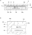
- the upper surface of the frame formed at the outer edge on the display surface side of the display panel of the display device is higher than the display surface, and a step portion having a height H, for example, between the upper surface of the frame and the display surface It is preferably used for a certain display device. Therefore, the second base material 14 of the transparent surface material 10 has an appropriate thickness corresponding to the stepped portion (for example, the thickness of the stepped portion in consideration of the thickness of the adhesive layer 16 and the resin layer 20).
- the first base material 12 is provided on the first base material 12 with the second base material 14 having an appropriate thickness) and having an outer shape smaller than that of the first base material 12. It is preferable that the stepped portion formed at the peripheral edge of the frame 106 and the stepped portion formed between the end surface 106 of the upper surface of the frame 106 and the display surface 104a are arranged to coincide with each other.
- the shear elastic modulus is 10 4 Pa or more, it is easy to suppress deformation of the adhesive layer 16 when the protective film 18 is peeled off. If the shear modulus is 10 7 Pa or less, the adhesive layer 16 can exhibit good adhesion when bonded to a display panel.
- the molecular mobility of the resin material forming the adhesive layer 16 is relatively high, when the display panel and the transparent surface material 10 are bonded together in a reduced pressure atmosphere, this is returned to the atmospheric pressure atmosphere.
- the volume of the voids tends to decrease due to the differential pressure between the pressure in the voids (pressure in the state of pressure) and the pressure applied to the adhesive layer 16 (atmospheric pressure).
- the gas in the voids whose volume has been reduced dissolves in the adhesive layer 16 and is easily absorbed.
- the weir-shaped portion 34 is made of a transparent resin formed by applying and curing a liquid weir-shaped portion-forming curable resin composition (hereinafter referred to as a second composition).
- the width of the weir portion 34 is preferably 0.5 to 2 mm, and more preferably 0.8 to 1.6 mm.
- the thickness of the weir-like portion 34 is substantially equal to the average thickness of the layer-like portion 36 excluding the region where the weir-like portion 34 and the layer-like portion 36 are close to each other, or 0.005 to less than the average thickness of the layer-like portion 36.
- the thickness is preferably 0.05 mm, more preferably 0.01 to 0.03 mm.
- the shear elastic modulus at 25 ° C. of the weir-shaped portion 34 is larger than the shear elastic modulus at 25 ° C. of the layered portion 36.
- the thickness of the protective film 18 is preferably 0.03 to 0.2 mm, and more preferably 0.05 to 0.1 mm when a relatively flexible film such as polyethylene and polypropylene is used. If the thickness of the protective film 18 is 0.03 mm or more, deformation of the protective film 18 can be suppressed when the protective film 18 is peeled from the adhesive layer 16. If the thickness of the protective film 18 is 0.2 mm or less, the protective film 18 is easily bent at the time of peeling and can be easily peeled off. Moreover, in the protective film 18, by providing a back layer on the side in contact with the adhesive layer 16, peeling from the adhesive layer 16 can be further facilitated.
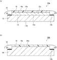
- the transparent base material 24 which integrated the 1st base material 12 and the 2nd base material like the transparent surface material 10b shown in FIG.3 (b).
- the transparent surface material 10 b has the transparent base material 24, and the adhesive layer 16 is formed on the upper surface 24 a of the transparent base material 24. Since the configuration is the same as that of the transparent surface material 10 shown in FIGS. 1A and 1B except that the light shielding portion 22 is formed on the end surface 24 b of the transparent base material 24, the details thereof are as follows. Description is omitted.
- the transparent base material 24 can be configured using, for example, the same material as the first base material 12, and can be formed by, for example, pressing, cutting, injection molding, or the like.
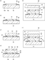
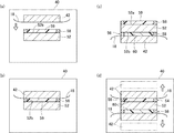
- FIG. 4A is a schematic cross-sectional views showing the method of manufacturing the transparent surface material shown in FIG. 1 (a) in the order of steps.
- the light shielding portion 22 is formed in the peripheral region 12 b of the first base material 12.
- the light shielding portion 22 is formed in a frame shape as shown in FIG.
- the weir 30 is formed so as to surround the periphery of the arrangement region 12 a of the second base material 14 so as to cover the inner edge of the light shielding unit 22.
- the dam 30 is formed in a frame shape having a predetermined width.
- the second composition when the second composition is a photocurable composition and is partially cured by irradiation with light at the same time as application or immediately after application, the second composition is second.
- the viscosity of the composition may be 5 to 500 Pa ⁇ s, and in that case, 10 to 100 Pa ⁇ s is preferable because the coating speed can be increased. If the viscosity is 10 Pa ⁇ s or more, the shape after application can be maintained in the time from application to light irradiation, and the height of the uncured weir can be sufficiently maintained. If the viscosity is 100 Pa ⁇ s or less, the height of the uncured weir-like portion can be sufficiently secured even if the coating speed is increased.
- the viscosity of the first composition and the viscosity of the second composition are measured using an E-type viscometer at a temperature of 25 ° C.
- FIG. 4 (e) a semi-finished product of the transparent face material 10 in which the resin composition 35 is formed on the face 14a of the second base material 14 (hereinafter referred to as a laminate) is shown in FIG. 4 (e). Then, it is transferred into the decompression chamber 40. In the decompression chamber 40, the protective film 18 is adhered to and held by the support surface member 42.
- the support surface member 42 is made of a glass plate, a resin plate, or the like, and is disposed above the resin composition 35.
- a known thermosetting device (not shown) or a photocuring device (not shown) may be provided in the decompression chamber 40 so that the thermosetting process or the photocuring process can be performed. .
- a vacuum pump (not shown) is connected to the decompression chamber 40, and the pressure is reduced to a predetermined pressure by the vacuum pump.
- the pressure in the decompression chamber 40 is, for example, 1 kPa or less, preferably 10 to 300 Pa, more preferably 15 to 100 Pa. If the pressure in the decompression chamber 40 is too low, each component (such as a curable compound, a photopolymerization initiator, a polymerization inhibitor, a chain transfer agent, and a light stabilizer) contained in the resin composition 35 is adversely affected. In addition, it takes time to bring the inside of the decompression chamber 40 to a predetermined pressure.
- the pressure in the decompression chamber 40 after releasing the decompression atmosphere is usually 80 to 120 kPa.
- the pressure in the decompression chamber 40 is most preferably atmospheric pressure because the resin composition 35 can be cured without requiring special equipment.
- a layered portion 36 is formed, and the support surface material 42 is peeled from the protective film 18, The transparent surface material 10 in which the adhesive layer 16 is protected by the protective film 18 is manufactured.
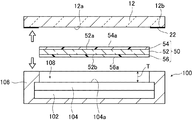
- the first base member 12 with the light shielding portion 22 formed in the peripheral region 12b and the LCD module 100 are prepared.
- the above-mentioned method (refer FIG. 4A) can be used for the formation method of the light shielding part 22.
- FIG. 4A the detailed description is abbreviate
- the uncured resin composition 59 is subjected to a predetermined curing process such as a heat curing process or a light curing process. Thereby, the 1st adhesion layer 54 and the 2nd adhesion layer 56 are formed (refer to Drawing 6 (d)).
- the formation process of the 1st adhesion layer 54 and the 2nd adhesion layer 56 is a process similar to the formation process of the adhesion layer 16 shown in FIG.4 (f), the detailed description is abbreviate
- the first adhesive layer 54 and the second adhesive layer 56 have a greater adhesive force of the protective film 18 than the support surface member 42. For this reason, when the support surface member 42 is moved away from the intermediate member 51, the protective film 18 is attached to the first adhesive layer 54 and the second adhesive layer 56.
- the manufacturing method of the transparent member 50 is not limited to the above-described method, and for example, it can be manufactured by the method shown in FIGS. 7 (a) to (d). In this case, detailed description of the same manufacturing apparatus and manufacturing steps as those of the manufacturing method of the transparent member 50 shown in FIGS. 6A to 6D is omitted.
- a dam-like portion 58 is formed on the outer edge of the back surface 52 b of the transparent substrate 52, and a resin composition 59 is formed in a region surrounded by the dam-like portion 58.
- the protective film 18 is transferred into the decompression chamber 40 and the protective film 18 held by the support surface member 42 is disposed above the resin composition 59.
- the inside of the decompression chamber 40 is decompressed to a predetermined pressure by a vacuum pump (not shown).
- the support surface member 42 is moved toward the resin composition 59 by the side of the back surface 52b, and the protective film 18 is closely_contact
- a predetermined time elapses at high pressure.
- the resin composition 59 on the back surface 52b side is subjected to a predetermined curing process such as a thermosetting process or a photocuring process. Thereby, the 2nd adhesion layer 56 is formed.
- the display surface can be suitably protected even when the step between the frame or the like and the display surface is large in the display device. It is useful for a display device equipped with a coordinate input device or the like.
Landscapes
- Engineering & Computer Science (AREA)
- Mechanical Engineering (AREA)
- Chemical & Material Sciences (AREA)
- Chemical Kinetics & Catalysis (AREA)
- General Chemical & Material Sciences (AREA)
- Liquid Crystal (AREA)
- Laminated Bodies (AREA)
- Adhesive Tapes (AREA)
- Devices For Indicating Variable Information By Combining Individual Elements (AREA)
Abstract
La présente invention se rapporte à un matériau de surface transparente pouvant protéger de manière satisfaisante une surface d'affichage même lorsqu'il y a une différence de niveau depuis une surface supérieure d'un cadre vers la surface d'affichage dans un dispositif d'affichage, et à un dispositif d'affichage qui utilise le matériau de surface transparente. Ce matériau de surface transparente possède un premier substrat transparent, un second substrat transparent disposé sur le premier substrat et ayant un contour plus petit que celui du premier substrat, une couche adhésive disposée sur le second substrat et un film protecteur disposé sur la couche adhésive.
Priority Applications (3)
| Application Number | Priority Date | Filing Date | Title |
|---|---|---|---|
| CN201480007567.XA CN104968491A (zh) | 2013-02-06 | 2014-02-05 | 透明面材以及使用该透明面材的显示装置 |
| JP2014560787A JPWO2014123165A1 (ja) | 2013-02-06 | 2014-02-05 | 透明面材およびそれを用いた表示装置 |
| US14/748,696 US20150314573A1 (en) | 2013-02-06 | 2015-06-24 | Transparent plate and display device using it |
Applications Claiming Priority (2)
| Application Number | Priority Date | Filing Date | Title |
|---|---|---|---|
| JP2013021662 | 2013-02-06 | ||
| JP2013-021662 | 2013-02-06 |
Related Child Applications (1)
| Application Number | Title | Priority Date | Filing Date |
|---|---|---|---|
| US14/748,696 Continuation US20150314573A1 (en) | 2013-02-06 | 2015-06-24 | Transparent plate and display device using it |
Publications (1)
| Publication Number | Publication Date |
|---|---|
| WO2014123165A1 true WO2014123165A1 (fr) | 2014-08-14 |
Family
ID=51299757
Family Applications (1)
| Application Number | Title | Priority Date | Filing Date |
|---|---|---|---|
| PCT/JP2014/052698 Ceased WO2014123165A1 (fr) | 2013-02-06 | 2014-02-05 | Matériau de surface transparente et dispositif d'affichage utilisant celui-ci |
Country Status (5)
| Country | Link |
|---|---|
| US (1) | US20150314573A1 (fr) |
| JP (1) | JPWO2014123165A1 (fr) |
| CN (1) | CN104968491A (fr) |
| TW (1) | TW201437039A (fr) |
| WO (1) | WO2014123165A1 (fr) |
Cited By (6)
| Publication number | Priority date | Publication date | Assignee | Title |
|---|---|---|---|---|
| TWI580004B (zh) * | 2014-10-17 | 2017-04-21 | 佳世達科技股份有限公司 | 平面顯示裝置及應用於其上之背光產生方法 |
| WO2018088300A1 (fr) * | 2016-11-11 | 2018-05-17 | バンドー化学株式会社 | Feuille adhésive transparente optique, stratifié, et dispositif d'affichage avec panneau tactile |
| WO2018200585A1 (fr) * | 2017-04-26 | 2018-11-01 | Eureka Therapeutics, Inc. | Cellules exprimant des récepteurs d'antigènes chimériques et des effecteurs secondaires et leurs utilisations |
| KR20190085327A (ko) * | 2018-01-10 | 2019-07-18 | 엘지이노텍 주식회사 | 디스플레이용 커버 윈도우 및 이를 포함하는 디스플레이 장치 |
| US10464988B2 (en) | 2015-10-23 | 2019-11-05 | Eureka Therapeutics, Inc. | Antibody/T-cell receptor chimeric constructs and uses thereof |
| US12570221B2 (en) * | 2020-10-15 | 2026-03-10 | Kyoraku Co., Ltd. | Panel |
Families Citing this family (6)
| Publication number | Priority date | Publication date | Assignee | Title |
|---|---|---|---|---|
| JP6555608B2 (ja) * | 2014-12-01 | 2019-08-07 | Tianma Japan株式会社 | ディスプレイ装置および電子機器 |
| TWI564769B (zh) * | 2015-11-20 | 2017-01-01 | 友達光電股份有限公司 | 觸控顯示裝置及其製造方法 |
| JP6662083B2 (ja) * | 2016-02-18 | 2020-03-11 | 凸版印刷株式会社 | 表示装置 |
| CN115113430A (zh) | 2016-05-24 | 2022-09-27 | 大日本印刷株式会社 | 调光装置 |
| US10033015B1 (en) | 2017-04-07 | 2018-07-24 | Motorola Mobility Llc | Flexible, optically clear, composite structures for foldable displays in mobile devices |
| CN114103088B (zh) * | 2021-11-26 | 2022-07-08 | 惠州深科达智能装备有限公司 | 一种导电膜贴附方法及设备 |
Citations (8)
| Publication number | Priority date | Publication date | Assignee | Title |
|---|---|---|---|---|
| JP2001134213A (ja) * | 1999-11-09 | 2001-05-18 | Seiko Epson Corp | 電気光学装置及びその製造方法 |
| JP2003150316A (ja) * | 2001-08-30 | 2003-05-23 | Nissha Printing Co Ltd | 再剥離可能な透明タッチパネルの実装構造とこれに用いる実装用シート |
| WO2006123616A1 (fr) * | 2005-05-16 | 2006-11-23 | Nissha Printing Co., Ltd. | Structure de fixation de panneau de protection amovible et feuille de fixation a utiliser avec |
| JP2007086290A (ja) * | 2005-09-21 | 2007-04-05 | Sanyo Epson Imaging Devices Corp | 電気光学装置、保護部材、電子機器 |
| JP2009093158A (ja) * | 2007-09-21 | 2009-04-30 | Toshiba Matsushita Display Technology Co Ltd | 表示素子 |
| JP2009098324A (ja) * | 2007-10-16 | 2009-05-07 | Epson Imaging Devices Corp | 表示装置、表示装置の製造方法、および電子機器 |
| JP2010122563A (ja) * | 2008-11-21 | 2010-06-03 | Hitachi Displays Ltd | 表示装置及びその製造方法 |
| JP2011164508A (ja) * | 2010-02-15 | 2011-08-25 | Sony Corp | 電気的固体装置の製造方法および電気的固体装置 |
Family Cites Families (2)
| Publication number | Priority date | Publication date | Assignee | Title |
|---|---|---|---|---|
| GB1359165A (en) * | 1971-05-21 | 1974-07-10 | Glaverbel | Panels incorporating a glass sheet and the manufacture thereof |
| JP4063945B2 (ja) * | 1998-03-19 | 2008-03-19 | リンテック株式会社 | 電波シールド材 |
-
2014
- 2014-02-05 CN CN201480007567.XA patent/CN104968491A/zh active Pending
- 2014-02-05 JP JP2014560787A patent/JPWO2014123165A1/ja active Pending
- 2014-02-05 TW TW103103776A patent/TW201437039A/zh unknown
- 2014-02-05 WO PCT/JP2014/052698 patent/WO2014123165A1/fr not_active Ceased
-
2015
- 2015-06-24 US US14/748,696 patent/US20150314573A1/en not_active Abandoned
Patent Citations (8)
| Publication number | Priority date | Publication date | Assignee | Title |
|---|---|---|---|---|
| JP2001134213A (ja) * | 1999-11-09 | 2001-05-18 | Seiko Epson Corp | 電気光学装置及びその製造方法 |
| JP2003150316A (ja) * | 2001-08-30 | 2003-05-23 | Nissha Printing Co Ltd | 再剥離可能な透明タッチパネルの実装構造とこれに用いる実装用シート |
| WO2006123616A1 (fr) * | 2005-05-16 | 2006-11-23 | Nissha Printing Co., Ltd. | Structure de fixation de panneau de protection amovible et feuille de fixation a utiliser avec |
| JP2007086290A (ja) * | 2005-09-21 | 2007-04-05 | Sanyo Epson Imaging Devices Corp | 電気光学装置、保護部材、電子機器 |
| JP2009093158A (ja) * | 2007-09-21 | 2009-04-30 | Toshiba Matsushita Display Technology Co Ltd | 表示素子 |
| JP2009098324A (ja) * | 2007-10-16 | 2009-05-07 | Epson Imaging Devices Corp | 表示装置、表示装置の製造方法、および電子機器 |
| JP2010122563A (ja) * | 2008-11-21 | 2010-06-03 | Hitachi Displays Ltd | 表示装置及びその製造方法 |
| JP2011164508A (ja) * | 2010-02-15 | 2011-08-25 | Sony Corp | 電気的固体装置の製造方法および電気的固体装置 |
Cited By (14)
| Publication number | Priority date | Publication date | Assignee | Title |
|---|---|---|---|---|
| TWI580004B (zh) * | 2014-10-17 | 2017-04-21 | 佳世達科技股份有限公司 | 平面顯示裝置及應用於其上之背光產生方法 |
| US11421013B2 (en) | 2015-10-23 | 2022-08-23 | Eureka Therapeutics, Inc. | Antibody/T-cell receptor chimeric constructs and uses thereof |
| US10464988B2 (en) | 2015-10-23 | 2019-11-05 | Eureka Therapeutics, Inc. | Antibody/T-cell receptor chimeric constructs and uses thereof |
| US10822389B2 (en) | 2015-10-23 | 2020-11-03 | Eureka Therapeutics, Inc. | Antibody/T-cell receptor chimeric constructs and uses thereof |
| US11976105B2 (en) | 2015-10-23 | 2024-05-07 | Eureka Therapeutics, Inc. | Antibody/T-cell receptor chimeric constructs and uses thereof |
| JP6383117B1 (ja) * | 2016-11-11 | 2018-08-29 | バンドー化学株式会社 | 積層体 |
| WO2018088300A1 (fr) * | 2016-11-11 | 2018-05-17 | バンドー化学株式会社 | Feuille adhésive transparente optique, stratifié, et dispositif d'affichage avec panneau tactile |
| WO2018200585A1 (fr) * | 2017-04-26 | 2018-11-01 | Eureka Therapeutics, Inc. | Cellules exprimant des récepteurs d'antigènes chimériques et des effecteurs secondaires et leurs utilisations |
| US10822413B2 (en) | 2017-04-26 | 2020-11-03 | Eureka Therapeutics, Inc. | Cells expressing chimeric activating receptors and chimeric stimulating receptors and uses thereof |
| US11613573B2 (en) | 2017-04-26 | 2023-03-28 | Eureka Therapeutics, Inc. | Chimeric antibody/T-cell receptor constructs and uses thereof |
| US11965021B2 (en) | 2017-04-26 | 2024-04-23 | Eureka Therapeutics, Inc. | Cells expressing chimeric activating receptors and chimeric stimulating receptors and uses thereof |
| KR20190085327A (ko) * | 2018-01-10 | 2019-07-18 | 엘지이노텍 주식회사 | 디스플레이용 커버 윈도우 및 이를 포함하는 디스플레이 장치 |
| KR102402800B1 (ko) * | 2018-01-10 | 2022-05-27 | 엘지이노텍 주식회사 | 디스플레이용 커버 윈도우 및 이를 포함하는 디스플레이 장치 |
| US12570221B2 (en) * | 2020-10-15 | 2026-03-10 | Kyoraku Co., Ltd. | Panel |
Also Published As
| Publication number | Publication date |
|---|---|
| TW201437039A (zh) | 2014-10-01 |
| JPWO2014123165A1 (ja) | 2017-02-02 |
| CN104968491A (zh) | 2015-10-07 |
| US20150314573A1 (en) | 2015-11-05 |
Similar Documents
| Publication | Publication Date | Title |
|---|---|---|
| WO2014123165A1 (fr) | Matériau de surface transparente et dispositif d'affichage utilisant celui-ci | |
| KR101536066B1 (ko) | 평면판을 구비한 표시 패널, 평면판을 구비한 표시 패널의 제조 방법 및 수지 조성물 | |
| JP5206953B2 (ja) | 画像表示装置及びその製造方法 | |
| US20150212350A1 (en) | Adhesive layer-equipped transparent surface material, display device, and production method therefor | |
| JP4940215B2 (ja) | 表示機器および表示機器の製造方法 | |
| CN203360361U (zh) | 一种显示装置及其光学胶带 | |
| JP2014056250A (ja) | 光硬化型樹脂組成物 | |
| US9731479B2 (en) | Display device and manufacturing method therefor | |
| JP2015232656A (ja) | 機器及びその製造方法 | |
| CN104703795B (zh) | 带粘附层的透明面材、其制造方法及显示装置 | |
| WO2014061478A1 (fr) | Matériau face transparente avec couche d'adhésion, et dispositif d'affichage | |
| TWI549830B (zh) | The manufacturing method of the layered body | |
| WO2012161078A1 (fr) | Film d'impression pour panneau tactile, verre de recouvrement pour panneau tactile, panneau d'affichage à cristaux liquides, terminal multifonction, et procédé de fabrication de film d'impression pour panneau tactile | |
| JP2015114624A (ja) | 粘着層付き透明面材 | |
| TW201346004A (zh) | 附黏著層之透明面材、顯示裝置及彼等之製造方法 | |
| TW201516530A (zh) | 電子裝置、電子裝置蓋板的組裝方法及黏接結構 | |
| JP2015205784A (ja) | 粘着層付きカバーガラス | |
| JP2015087405A (ja) | 表示装置及びその製造方法 | |
| JP2012230304A (ja) | 液晶表示用保護シートの製造方法、液晶表示用保護シート、液晶表示装置の製造方法、液晶表示装置 | |
| JP2019112609A (ja) | 粘着層付き透明面材および表示装置 | |
| CN103376585A (zh) | 液晶显示装置的制造方法 | |
| CN101702402A (zh) | 防溢胶装置及使用该防溢胶装置的基板贴合方法 | |
| JP2016126283A (ja) | 表示装置、および、表示装置の製造方法 | |
| JP2017198763A (ja) | 前面板を有する画像表示パネル、およびその製造方法 |
Legal Events
| Date | Code | Title | Description |
|---|---|---|---|
| 121 | Ep: the epo has been informed by wipo that ep was designated in this application |
Ref document number: 14749408 Country of ref document: EP Kind code of ref document: A1 |
|
| ENP | Entry into the national phase |
Ref document number: 2014560787 Country of ref document: JP Kind code of ref document: A |
|
| NENP | Non-entry into the national phase |
Ref country code: DE |
|
| 122 | Ep: pct application non-entry in european phase |
Ref document number: 14749408 Country of ref document: EP Kind code of ref document: A1 |