WO2014129375A1 - Appareil électronique et système de traitement d'informations - Google Patents
Appareil électronique et système de traitement d'informations Download PDFInfo
- Publication number
- WO2014129375A1 WO2014129375A1 PCT/JP2014/053302 JP2014053302W WO2014129375A1 WO 2014129375 A1 WO2014129375 A1 WO 2014129375A1 JP 2014053302 W JP2014053302 W JP 2014053302W WO 2014129375 A1 WO2014129375 A1 WO 2014129375A1
- Authority
- WO
- WIPO (PCT)
- Prior art keywords
- touch panel
- transmission
- reception
- receiving
- drive
- Prior art date
- Legal status (The legal status is an assumption and is not a legal conclusion. Google has not performed a legal analysis and makes no representation as to the accuracy of the status listed.)
- Ceased
Links
Images
















Classifications
-
- G—PHYSICS
- G06—COMPUTING OR CALCULATING; COUNTING
- G06F—ELECTRIC DIGITAL DATA PROCESSING
- G06F3/00—Input arrangements for transferring data to be processed into a form capable of being handled by the computer; Output arrangements for transferring data from processing unit to output unit, e.g. interface arrangements
- G06F3/01—Input arrangements or combined input and output arrangements for interaction between user and computer
- G06F3/03—Arrangements for converting the position or the displacement of a member into a coded form
- G06F3/041—Digitisers, e.g. for touch screens or touch pads, characterised by the transducing means
- G06F3/044—Digitisers, e.g. for touch screens or touch pads, characterised by the transducing means by capacitive means
- G06F3/0446—Digitisers, e.g. for touch screens or touch pads, characterised by the transducing means by capacitive means using a grid-like structure of electrodes in at least two directions, e.g. using row and column electrodes
-
- G—PHYSICS
- G06—COMPUTING OR CALCULATING; COUNTING
- G06F—ELECTRIC DIGITAL DATA PROCESSING
- G06F3/00—Input arrangements for transferring data to be processed into a form capable of being handled by the computer; Output arrangements for transferring data from processing unit to output unit, e.g. interface arrangements
- G06F3/01—Input arrangements or combined input and output arrangements for interaction between user and computer
- G06F3/03—Arrangements for converting the position or the displacement of a member into a coded form
- G06F3/041—Digitisers, e.g. for touch screens or touch pads, characterised by the transducing means
- G06F3/0416—Control or interface arrangements specially adapted for digitisers
- G06F3/04166—Details of scanning methods, e.g. sampling time, grouping of sub areas or time sharing with display driving
-
- G—PHYSICS
- G06—COMPUTING OR CALCULATING; COUNTING
- G06F—ELECTRIC DIGITAL DATA PROCESSING
- G06F3/00—Input arrangements for transferring data to be processed into a form capable of being handled by the computer; Output arrangements for transferring data from processing unit to output unit, e.g. interface arrangements
- G06F3/01—Input arrangements or combined input and output arrangements for interaction between user and computer
- G06F3/03—Arrangements for converting the position or the displacement of a member into a coded form
- G06F3/041—Digitisers, e.g. for touch screens or touch pads, characterised by the transducing means
- G06F3/044—Digitisers, e.g. for touch screens or touch pads, characterised by the transducing means by capacitive means
- G06F3/0443—Digitisers, e.g. for touch screens or touch pads, characterised by the transducing means by capacitive means using a single layer of sensing electrodes
Definitions
- the present invention relates to an electronic device or the like that can detect a contacted or approached object.
- Patent Document 1 is an example.
- Patent Document 1 discloses a table-type screen device 200 as shown in FIG.
- the positions of the camera 231 and the printer 235 placed on the screen 215 are detected by the position detection unit 223 via the touch panel 216, and the communication unit 225 is connected from the camera 231 in accordance with a predetermined command operation.
- the image data 233 is transferred to the printer 235.
- an image 233a indicating the transfer progress of the image data is displayed between the position of the camera 231 and the position of the printer 235 on the screen 215.
- Japanese Patent Publication Japanese Patent Laid-Open No. 2011-221542 (published on November 4, 2011)” US Pat. No. 6,452,514 (registered July 17, 2002) Japanese Patent Gazette “Patent No. 4927216 (registered on Feb. 17, 2012)”
- the positions of the electronic devices such as the camera 231 and the printer 235 on the screen 215 are detected via the touch panel 216, but the detection accuracy is such that image data transfer history can be displayed between the electronic devices. That's fine.
- the table-type screen device 200 only needs to be able to detect the position of the electronic device placed on the screen 215 to such an extent that the display can be performed.
- the drive line or sense line formed by the electrode group included in the touch panel 216 There is no need to be able to detect a positional relationship finer than the line pitch of minutes, and such a configuration is not disclosed in Patent Document 1.
- the present invention has been made to solve the above-described problem, and an object thereof is to provide an electronic device that can accurately detect the relative positional relationship of an electronic device including a touch panel. .
- an electronic device is an electronic device as a receiving device including a receiving-side touch panel that is a capacitive touch panel that detects contact or approach of an object.
- the receiving-side sense line included in the receiving-side touch panel can receive a pulse signal applied to the transmitting-side drive line included in the transmitting-side touch panel, which is a capacitive touch panel included in the transmitting device that is in contact with or close to the own device. Further, by determining which one of a plurality of reception side sense lines provided in the reception side touch panel has received the pulse signal transmitted from the transmission side drive line, the transmission device for the own device It is the structure provided with the determination means which determines the position of.
- an electronic device includes a transmission-side touch panel that is a capacitive touch panel that detects contact or approach of an object, and a transmission-side housing in which the transmission-side touch panel is assembled.
- the shortest distance between the transmission-side touch panel and the outer surface of the transmission-side housing is not more than a detectable distance at which the transmission-side touch panel can detect contact or approach of the object to the outer surface,
- An electronic device as a transmission device which is capable of receiving a pulse signal applied to a transmission-side drive line included in the transmission-side touch panel for detecting contact or approach of the object.
- the receiving side touch panel which is a capacitive touch panel included in the receiving device, receives the signal.
- Ri is a configuration that enables the determination of the position of the own apparatus by the receiving apparatus.
- the electronic device according to one aspect of the present invention has an effect that the position of the counterpart device relative to the own device can be specified with high accuracy.
- FIG. 1 It is a top view which shows an example of an electrostatic capacitance type touch panel
- (a) is a top view for demonstrating the electrode structure of a touch panel
- (b) is AB sectional drawing of (a)
- (c) is a figure for demonstrating operation
- It is a block diagram of the position detection circuit of a mutual capacitive touch panel. 10 is a timing chart showing the operation of the circuit of FIG.
- 2 is a diagram illustrating an example of an information processing system including the display device
- (a) to (d) are diagrams illustrating an example of a positional relationship of the display device.
- FIG. 1 It is a block diagram which shows the equivalent circuit of a mutual capacitive touch panel.
- A)-(c) is a figure for demonstrating the drive principle of a mutual capacitive touch panel. It is a figure for demonstrating the drive principle of a sequential drive system. It is a figure for demonstrating the drive principle of an orthogonal sequence drive system. It is a figure for demonstrating the drive principle of an orthogonal sequence drive system. It is a figure for demonstrating the effect which can shorten the sensing time of a touch panel by using parallel drive, (a) is a figure which shows the sensing time in the case of sequential drive, (b) is the case in the case of parallel drive It is a figure which shows sensing time.
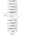
- FIG. 1 It is a figure which shows an example of the functional block of the control part with which the display apparatus (transmission apparatus) which concerns on one Embodiment of this invention is provided. It is a figure which shows an example of the drive method at the time of a position detection, (a) is a figure which shows the drive method of a transmitter, (b) is a figure which shows the drive method of a receiver. It is a flowchart which shows the flow of the process in a transmission apparatus. It is a figure which shows an example of signal distribution when a receiving device detects the contact or approach of a transmitting device. It is a flowchart which shows the flow of the process in a receiver.
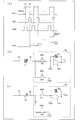
- (A) is a figure which shows the equivalent circuit of a synchronous adjustment circuit
- (b) is a figure which shows an example of the input-output table which an exclusive OR circuit refers. It is a figure which shows the correlation output signal which the input signal and the replica pattern signal produced
- (A) And (b) is a timing chart which shows the timing of a touch panel operation
- (A) is a diagram showing a schematic diagram and an equivalent circuit when two display devices (transmitting device and receiving device) are not adjacent, and (b) is a schematic diagram when two display devices are adjacent.
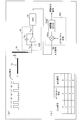
- (A) And (b) is a figure which shows an example of the positional relationship of a transmission apparatus and a receiving apparatus
- (c) is a figure which shows an example of a position detection table.
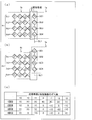
- (A) And (c) is the schematic which shows the equivalent circuit at the time of position detection
- (b) And (d) is a figure which shows an example of the signal distribution corresponding to (a) and (c), respectively. is there. It is a figure which shows the relationship between the electrode arrangement
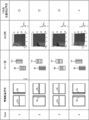
- (A) to (d) show examples of equivalent circuits corresponding to the cases 1 to 4 shown in FIG.
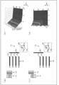
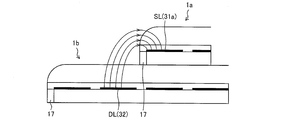
- FIG. 14 is a schematic cross-sectional view of a transmission device and a reception device showing the state of FIG. It is a figure which shows an example of the signal distribution at the time of position detection.
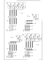
- FIG. 14 is a schematic cross-sectional view of a transmission device and a reception device showing the state of FIG. It is a figure which shows the relationship between the electrode arrangement
- (A)-(c) is a figure which shows the positional relationship of a transmission apparatus and a receiving apparatus
- (d) is a figure which shows an example of an inclination detection table.
- (A) to (d) show examples of equivalent circuits corresponding to the respective angles shown in (d) of FIG.
- (A)-(d) is a figure which shows an example of the signal distribution corresponding to each of each angle shown by (d) of FIG. It is a figure which shows an equivalent circuit when the data communication between touch panels is performed. It is a figure which shows an example of the conventional table type screen apparatus.
- FIGS. 1 to 52 An embodiment of the present invention will be described with reference to FIGS. 1 to 52 as follows.
- an information processing system 5 including two display devices 1 (electronic devices) including a touch panel 14 (described later) will be described with reference to FIG.
- the display device 1 can be replaced with a display device 2 or 3 (electronic device) described later.
- one display device 1 detects that the other display device has touched or approached
- a drive signal applied on the touch panel of the other display device 1 (transmission side) Then, reception (sensing) is performed on the touch panel of one display device.
- reception (sensing) is performed on the touch panel of one display device.
- the information processing system 5 constructs a position detection system including the two display devices.
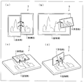
- FIG. 13 is a diagram showing an outline of the positional relationship between the two display devices 1.
- the display devices 1 are overlapped with each other, and the display area side of one display device 1 and the back surface of the other display device 1 (one surface of the casing opposite to the display area of the own device) face each other.
- the display devices 1 overlap each other and the display areas of the two display devices 1 face each other (see (c) of FIG. 13)
- the side surface of the other display device 1 is adjacent to one display device 1 (when the other display device 1 is placed upright on one display device 1) (( d))
- the display device 1 serving as the reception side and the transmission side may have a relationship opposite to the relationship illustrated in FIG.
- the display device 1 that can be a transmission-side device and a reception-side device will be described.
- the display devices 1 to 3 are realized by a liquid crystal display.
- the present invention is not limited to this, and the display devices 1 to 3 may be configured by a plasma display, an organic EL display, a field emission display, or the like.
- the display devices 1 to 3 are described as having a rectangular plate-like upper surface unless otherwise specified.
- the present invention is not limited to this, and the upper surface may be an elliptical shape, a circular shape, or the like.
- it may be a shape having irregularities on the surface instead of the plate-like member. That is, any shape may be used as long as the function described below can be implemented.
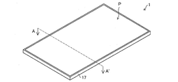
- FIG. 3 is a perspective view illustrating an example of a schematic configuration of a mobile terminal including the display device 1. 4 shows an example of a schematic configuration of the display device 1, and is a schematic cross-sectional view when the display device 1 shown in FIG. 3 is cut along the line AA ′.
- the display device 1 as a mobile terminal is a device that displays an image and can acquire an input operation on the image. As shown in FIG. 3, the shape of the display device 1 is defined by the housing 17, and an image is displayed in the display area P of the display screen (display panel 12).
- the display device 1 includes a display panel 12, a transparent adhesive layer (OCA) 13, a touch panel 14 (operation detection member), a transparent adhesive layer 15, and a backlight 11.
- a cover glass 16 is laminated in this order. Further, these members are supported by a housing 17 provided in the display device 1. That is, the housing 17 stores the display panel 12 and the touch panel 14. In other words, the display panel 12 and the touch panel 14 are assembled to the housing 17.
- the display panel 12 can adopt a known configuration.
- the display panel 12 includes an insulating active matrix substrate (not shown) made of glass or the like and an optically transparent counter substrate (not shown) made of glass facing the active matrix substrate at a predetermined interval. And a liquid crystal layer sandwiched between the active matrix substrate and the counter substrate.
- the liquid crystal layer various types of liquid crystal layers can be used.
- two deflecting plates 12 a and 12 d are provided so as to sandwich a TFT layer 12 b having a thin film transistor (TFT), thereby enabling gradation display of an image.
- TFT thin film transistor
- a color filter 12c is provided on the counter substrate side, so that color display is possible.
- the display panel 12 is provided with data signal lines extending in the column direction, scanning signal lines extending in the row direction and capacitive wiring, and pixels arranged in the row and column directions. Various signal lines are provided on the active matrix substrate.
- each pixel is the same, and at least one pixel electrode is provided corresponding to one pixel, and one data signal line, one scanning signal line, and one capacitor wiring are provided.
- the pixel electrode is connected to the data signal line through the thin film transistor disposed in the TFT layer 12b connected to the scanning signal line, and the counter electrode provided on the counter substrate A liquid crystal capacitor is formed between the two.
- the thin film transistor provided in each pixel has a source electrode connected to the pixel electrode, a drain electrode connected to the data signal line, and a gate electrode connected to the scanning signal line.
- the transistor is controlled to be turned on / off by the scanning signal (gate signal) supplied from the scanning signal line, and a voltage corresponding to the data signal supplied to the data signal line is applied to the liquid crystal layer, and the transistor is turned off. The voltage is held.
- the display panel 12 is controlled by various drive circuits and display control circuits (none of these circuits are shown) included in the display device 1.
- Examples of the various drive circuits include a data signal line drive circuit and a scanning signal line drive circuit.
- the display panel 12 is controlled by these circuits, whereby an image is displayed in the display area P.
- the display control circuit detects image display timing based on a timing control signal supplied from the timing controller, and displays an image on the display panel 12 based on display data and a synchronization signal input from the outside.
- a display control signal for displaying (video) is generated. Then, the generated display control signal is supplied to various drive circuits to control operations of the various drive circuits.
- the scanning signal line driving circuit sequentially supplies a scanning signal (gate signal) to each scanning signal line based on the display control signal output from the display control circuit. Accordingly, a transistor whose gate electrode is a part of the scanning signal line to which the scanning signal is supplied is turned on.
- the data signal line driving circuit supplies a data signal to the data signal line based on the display control signal. As a result, a voltage corresponding to the data signal is applied to the liquid crystal layer through the transistor in the on state, and image information is written.
- the backlight 11 makes display light incident on the display panel 12.
- the backlight 11 may be externally attached to the display device 1.
- the touch panel 14 is provided so as to be superimposed on the display panel 12, and is a member that detects contact or approach of a detection target object (target object) such as a user's finger or pointing pen at least in the display area P of the display panel 12. It is. As a result, it is possible to acquire a user's input operation on the image displayed in the display area P and perform operation control of a predetermined function (various applications) based on the input operation.
- a detection target object such as a user's finger or pointing pen
- a capacitive touch panel (capacitive touch panel) can be employed.
- a transparent adhesive layer 13 is provided between the display panel 12 and the touch panel 14, and the display panel 12 and the touch panel 14 are fixed. It is possible to provide an air layer (air gap) instead of the transparent adhesive layer 13, but in this case, the interface reflection between the transparent adhesive layer 13 and the touch panel 14 increases, so that an environment where external light exists is present. When the display device 1 is used, there is a possibility that an adverse effect such as a decrease in the contrast of the displayed image may occur.
- the transparent adhesive layer 13 as in this embodiment, the optical characteristics of the display device 1 can be improved.
- the film thickness (gap) controllability of each layer can also be improved. That is, in the display device 1 according to the present embodiment, it is preferable that the transparent adhesive layer 13 is provided.
- the transparent adhesive layer 15 is provided between the touch panel 14 and the cover glass 16, and fixes the touch panel 14 and the cover glass 16.
- the cover glass 16 is a transparent plate-like member, and is disposed so as to cover the touch panel 14 in order to protect the touch panel 14 from external factors.
- the shape of the cover glass 16 is rectangular.
- the shape is not limited to this, and the end portion (outer edge) may have a cutout shape.
- the outer edge of the display device 1 Detection accuracy on the outer surface A of the display device 1 other than the display area P (see FIG. 2) can be increased.
- the housing 17 stores the display panel 12 and the touch panel 14 as described above.
- the housing 17 is made of a material having a high dielectric constant.
- the “material having a high dielectric constant” refers to a material having a dielectric constant that makes it easy for the touch panel 14 to detect contact or approach of a finger or the like to the outer edge of the display device 1.
- glass used as the cover glass 16 having a relative dielectric constant of about 6 glass used for the touch panel 14.
- the present invention is not limited to this, and other resins having a relative dielectric constant of about 3 may be used. That is, it is preferable to use a material having a relative permittivity of 3 or more (preferably 6 or more) for the casing 17 to facilitate the detection.
- Such a material having a high dielectric constant is used for the casing 17, so that the detection accuracy at the outer edge of the display device 1 can be increased.
- the thickness of each member of the display device 1 according to the embodiment is as follows.
- the thickness of the backlight 11 is 0.74 mm
- the thickness of the deflecting plate 12a is 0.15 mm
- the thickness of the TFT layer 12b is 0.25 mm
- the thickness of the color filter 12c is 0.15 mm
- the thickness of the deflecting plate 12d is 0. 11 mm
- the thickness of the transparent adhesive layer 13 is 0.2 mm
- the thickness of the touch panel 14 is 0.4 mm
- the thickness of the transparent adhesive layer 15 is 0.1 mm
- the thickness h1 of the cover glass 16 is 2 mm.
- the thickness h2 from the surface of the cover glass 16 to the interface between the touch panel 14 and the transparent adhesive layer 13 is 2.5 mm
- the thickness h3 from the surface of the cover glass 16 to the interface between the color filter 12c and the TFT layer 12b is 2. 96 mm.
- the above-described thickness is merely an example, and may be appropriately changed depending on the size of the mobile terminal including the display device 1.
- the thickness of the display panel 12 is 0.86 mm, it may be about 0.7 mm, and the thickness of the touch panel 14 may be about 0.7 mm.
- the horizontal length (width) of the housing 17 is set to a length that allows the touch panel 14 to detect contact or approach of a finger or the like to the outer surface (end surface) of the housing 17 as will be described later. Has been.
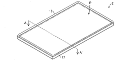
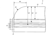
- FIG. 5 is a perspective view illustrating an example of a schematic configuration of a mobile terminal including the display device 2 which is a modification of FIG. 6 shows an example of a schematic configuration of the display device 2, and is a schematic cross-sectional view when the display device 2 shown in FIG. 5 is cut along the line AA ′.
- the display device 2 is different from the display device 1 in that a lens 18 is provided instead of the cover glass 16.
- the function is the same as each member of the display device 1. Therefore, only the parts different from the display device 1 will be mainly described, and the other description will be omitted.
- a lens 18 is laminated on the touch panel 14.
- the lens 18 is a transparent plate-like member, and is disposed so as to cover the touch panel 14 in order to protect the touch panel 14 from external factors.
- the lens 18 has a notch R1 (notch shape) at its end (outer edge), and changes the traveling direction of light emitted from the display panel 12.
- the detection accuracy of the touch panel 14 at the outer edge of the display device 2 can be increased as described above. Further, the traveling direction of the light emitted from the pixels arranged on the outer edge of the display panel 12 is changed by the cutout portion R1, and is emitted from the area outside the pixel (non-display area). Therefore, the viewing angle of the image (display area when viewed from the user) can be enlarged. In the case where the enlargement function is not necessary, it is not always necessary to have the cutout portion R1.
- the thickness of each member of the display device 2 is the same as that of the display device 1 except for the cover glass 16.
- the thickness h1 ′ of the lens 18 is 2.13 mm
- the thickness h2 ′ from the surface of the lens 18 to the interface between the touch panel 14 and the transparent adhesive layer 13 is 2.63 mm
- the color filter 12c and the TFT layer 12b from the surface of the lens 18 The thickness h3 ′ to the interface is 3.09 mm.
- the width w1 of the notch R1 is 2.1 mm. Similar to the display device 1, these thicknesses are merely examples, and may be appropriately changed depending on the size of the mobile terminal including the display device 2.
- a multifunctional mobile phone so-called smart phone
- a tablet as a portable terminal to which the display device 1 or 2 is applied, a multifunctional mobile phone (so-called smart phone), a tablet, and the like can be given.
- the display devices 1 and 2 can be widely applied to devices that can acquire image display and input operations on the image, such as televisions and monitors.
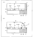
- FIG. 2 is a cross-sectional view illustrating an example of a schematic configuration of the display device 1 and the like for explaining the display device 1 and the like according to an embodiment of the present invention, and (a) is a display including a cover glass 16.
- FIG. 2 is a diagram illustrating a schematic configuration of the device 1
- FIG. 5B is a diagram illustrating a schematic configuration of a display device 2 including a lens 18.
- ⁇ Display device 1 (portable terminal)> First, a schematic configuration of the display device 1 will be described with reference to FIG. Here, in order to simplify the explanation, the illustration of the configuration such as the transparent adhesive layer 15 shown in FIG. 4 is omitted.
- the touch panel 14 includes a detection electrode 31 and a drive electrode 32 as an electrode group for detecting contact or approach of a finger or the like on a substrate. And it has the detection electrode 31a and the drive electrode 32a as an outer edge electrode group arrange
- a first wiring storage portion 12A in which various wirings of the display panel 12 can be disposed is provided between the display panel 12 and the inner surface of the housing 17. Between the touch panel 14 and the housing
- positioned are provided.
- the shortest distance d between the touch panel 14 and the outer surface A of the casing 17 other than the display area P is the touch panel 14 to the outer surface A.
- the distance is less than the detectable distance capable of detecting the contact or approach of a finger or the like. According to this configuration, contact or approach of a finger or the like to the outer surface A of the casing 17 other than the display area P can be detected. Accordingly, since it is not always necessary to detect contact or approach of a finger or the like on the image displayed on the display panel 12, an operation with a finger or the like can be performed while preventing the visibility and operability of the image from being deteriorated. It can be acquired.
- the said outer surface A since the touch or approach of a finger
- the shortest distance d is specifically a first distance between each of the detection electrode 31a and the drive electrode 32a as the outer edge electrode group provided in the touch panel 14 and the outer surface A, as shown in FIG. It is.
- the first distance (shortest distance d) is perpendicular to the display panel 12 and the touch panel 14 (specifically, the detection electrode 31 and the drive electrode 32) and the outer surface of the cover glass 16 (contact of a finger or the like).
- the second distance d1 is equal to or less than the second distance d1 that is a distance between the surface and the upper surface of the display device 1. In the case of this configuration, contact or approach of a finger or the like to the outer surface A of the housing 17 can be reliably detected.
- the display device 1 has a narrow frame (frameless) in which the shortest distance d is defined so that contact or approach of a finger or the like to the outer surface A of the housing 17 can be detected. It is a configuration. Thereby, it is possible to sense contact or approach of a finger or the like to the outer surface A (that is, the outer edge (terminal edge) of the display device 1). In addition, the design of the display device 1 can be improved by narrowing the frame.
- At least one end surface that is a part of the outer surface A of the housing 17 may be such that the shortest distance d is equal to or shorter than the detectable distance. In this case, at least contact or approach of a finger or the like to the one end surface can be detected.
- Display device 2 (portable terminal)> Next, a schematic configuration of the display device 2 will be described with reference to FIG. Here, in order to simplify the explanation, the illustration of the configuration such as the transparent adhesive layer 15 shown in FIG. 6 is omitted. As described above, the display device 2 is different from the display device 1 in that the lens 18 is provided instead of the cover glass 16.
- the shortest distance d between the touch panel 14 and the outer surface B of the casing 17 other than the display area P detects that the touch panel 14 touches or approaches the outer surface B.
- the distance is less than the detectable distance that can be detected. Also in this case, as in the display device 1, it is possible to detect contact or approach of a finger or the like to the outer surface B of the housing 17 other than the display area P.
- the outer surface B includes the outer surface of the notch R1 of the lens 18 in addition to the outer surface of the housing 17 (the outer surface A shown in FIG. 2A). That is, in the present embodiment, the outer surface B of the housing 17 is defined as including the two outer surfaces.
- the shortest distance d (first distance) is, as shown in FIG. 2B, the outer side of each of the detection electrode 31 a and the drive electrode 32 a as the outer edge electrode group included in the touch panel 14. It is the distance to the surface B. And like the display apparatus 1, it is preferable that this shortest distance d is 2nd distance d1 or less, and if the shortest distance d is below a detectable distance in at least one end surface which is a part of the outer surface B. Good.
- the display device 3 is not shown in FIG. 7, the display device 12 and the display panel 12 are provided so as to overlap with the display panel 12, as in the display devices 1 and 2.
- the touch panel 14 (first operation detection member) that detects contact or approach of a finger or the like, and a housing 17 that stores the display panel 12 and the touch panel 14 are provided.
- the shortest distance d is equal to or shorter than a detectable distance at which the touch panel 14 can detect contact or approach of a finger or the like to the outer surface A or B. Therefore, it is not necessary to provide a detection member for detecting the contact to the outer surface A or B or the like.
- the present invention is not limited to this configuration, and an outer surface A or B of the housing 17 is provided by providing a member different from the touch panel 14, that is, the touch panel 14a (second operation detecting member), like the display device 3 shown in FIG. It may be configured to detect contact or approach of a finger or the like.
- the touch panel 14 a has a configuration in which the detection electrodes 31 and the drive electrodes 32 are alternately and arranged in a row, but the height is not limited to this, and the height of the end surface (side surface) of the housing 17.
- the height is not limited to this, and the height of the end surface (side surface) of the housing 17.
- it may be configured to have a plurality of rows. In this case, since the interval between the detection electrodes 31 and the interval between the drive electrodes 32 are smaller than those of the touch panel 14a shown in FIG. 7, the position of the counterpart device relative to the own device can be detected with higher accuracy. .
- touch panel 14 Since the touch panels 14 and 14a have the same configuration except for the arrangement, the touch panel 14 will be described as an example in the following description.
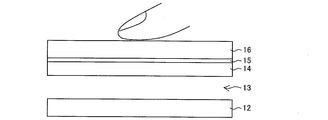
- FIG. 8 is a schematic cross-sectional view for explaining a schematic configuration of the touch panel 14 included in the display device 1 or the like.
- the display device 1 or the like includes the display panel 12, the transparent adhesive layer 13, the touch panel 14, the transparent adhesive layer 15, and the cover glass 16 (or the lens 18).
- the touch panel function is realized by these configurations.
- a capacitive touch panel is suitable.
- the capacitive touch panel it is possible to perform processing such as detection of the position of a partner device that has touched or approached, data communication with the partner device via the touch panel 14, as will be described later.
- various types of touch panels can be used without being limited to capacitive touch panels.
- a configuration in which a capacitive touch panel is used will be described below.
- In-cell type It may be a touch panel.
- the capacitive touch panel the capacitance when a finger or an input pen is brought into contact with the surface of the display device 1 or the like (the surface of the cover glass 16 or the lens 18 and the outer surfaces A and B). The contact position is detected by detecting the change. For this reason, the contact position can be detected by a simple operation.
- FIG. 9 shows an example of a capacitive touch panel.
- 9A is a plan view for explaining the electrode configuration of the touch panel
- FIG. 9B is a cross-sectional view taken along the line AB of FIG. 9A
- FIG. ) Is a diagram for explaining the operation of the touch panel when a finger (detection target) is touched on the touch panel.
- reference numeral 21 denotes a substrate made of a transparent insulator (dielectric), and a plurality of detection electrodes 31 and a plurality of drive electrodes 32 are provided on one surface of the substrate 21.
- a cover glass 16 is provided so as to cover the surface on which the detection electrode 31 and the drive electrode 32 are provided.
- the cover glass 16 is made of an insulator having a predetermined dielectric constant, for example, transparent glass.
- the plurality of drive electrodes 32 are connected in the X-axis direction for each row, and the plurality of detection electrodes 31 are connected to each column. Each is connected in the Y-axis direction.
- FIG. 9B when a drive voltage is applied to the drive electrode 32 and the detection electrode 31, an electrostatic is applied between the drive electrode 32 and the detection electrode 31 via the substrate 21 and the cover glass 16. A capacitance is formed, and electric lines of force as shown are formed.
- a position detection circuit for detecting the coordinate position of the detection object a known circuit (for example, see Patent Document 2) can be used, and is not particularly limited.
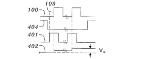
- FIG. 10 is a circuit configuration diagram of a mutual capacitance system, which is the mainstream of a capacitive touch panel, according to Patent Document 2, and FIG. 11 is a timing chart showing the operation of the circuit.
- a transmission electrode (drive electrode) 100 and a reception electrode (detection electrode) 104 are coupled by a cross capacitor 105.
- a switch 401, a storage capacitor 402 (corresponding to a capacitance Cf), a reset switch 404, And an output amplifier 403 is provided on the reception electrode side.
- the transmission electrode 100 generates 109 rectangular waveforms by the amplifier 101. First, reset is performed and measurement is performed after charge transfer and hold are repeated.
- the cross capacitance 105 changes depending on the presence or absence of a finger (for example, the cross capacitance is reduced by placing the finger), the position touched by the fingertip can be detected by measuring the difference in output voltage. it can.
- FIG. 12 is a top view showing a schematic configuration of the touch panel 14 according to the present embodiment.
- the touch panel 14 includes, on a substrate 21, a detection electrode 31 and a drive electrode 32 as an electrode group for detecting contact or approach of a finger or the like in a matrix. And it has the detection electrode 31a and the drive electrode 32a as an outer edge electrode group arrange
- the control of the detection electrode 31 and the drive electrode 32, that is, the circuit control shown in FIGS. 10 and 11 is performed by a TP controller (touch panel controller) 33.
- TP controller touch panel controller
- the display device 1 and the like according to the present embodiment are configured to detect contact or approach of a finger or the like to the outer surface A or B of the housing 17. Therefore, it is preferable that the 2nd wiring storage part 14A (frame wiring width w0 of the touch panel 14) of the touch panel 14 is 1 mm or less in the case of the display apparatuses 1 and 2 applied as a portable terminal.
- each electrode and the second wiring storage portion 14A are arranged so as not to disturb the light path of the light emitted from the display panel 12.
- a self-capacitance system can be applied in addition to the mutual capacity system described above.
- the TP controller 33 applies a pulse signal to each of the plurality of first electrode lines and the plurality of second electrode lines that intersect perpendicularly. Then, a capacitance (self-capacitance) formed between the first electrode line and the detection target is detected, and a capacitance (self-capacitance) formed between the second electrode line and the detection target is detected.
- the contact or approach position of the detection target is specified.
- the self-capacitance method it is limited to detection of only a single touch (single point simultaneous input), and the S / N ratio is lowered due to parasitic capacitance.
- the mutual capacitance method it is possible to detect multi-touch (simultaneous input of a plurality of points), cancel the parasitic capacitance by the charge transfer technique, and improve the S / N ratio.
- FIG. 14 is a configuration diagram showing an equivalent circuit of the mutual capacitance type touch panel 14.
- the touch panel 14 includes a plurality of detection electrodes 31 and a plurality of drive electrodes 32 as described above, and a plurality of sense lines SL (n) are arranged by arranging the plurality of detection electrodes 31. ), And a plurality of drive lines DL1 to DLn are formed by arranging a plurality of drive electrodes 32.
- a drive line drive circuit 41 is connected to each drive line DL1 to DLn of the touch panel 14, and a sense line drive circuit 42 is connected to each sense line SL (n).
- the circuit 41 and the sense line driving circuit 42 are driven under the control of the TP controller 33.
- a variable capacitance (capacitance) Cf whose capacitance changes due to the touch of a finger or the like that is the detection target is present. It is formed.
- the sense line driving circuit 42 is coupled to an operational amplifier 421 having one input grounded, an integration capacitor Cint disposed between the output of the operational amplifier 421 and the other input, and the other input of the operational amplifier 421. Transistor SW1 and another transistor SW2 connected in parallel with the transistor SW1. The circuit configuration of the sense line driving circuit 42 will be described later with reference to FIG.
- each sense line driving circuit 42 is connected to the ADC 43.
- An output from the capacitance Cf (capacitance Cf for each sense line SL) integrated by each sense line driving circuit 42 is supplied to the ADC 43.
- the ADC 43 performs AD conversion on the output from the capacitance Cf integrated by the sense line driving circuit 42 and supplies the converted signal to the control unit 50 or the control unit 60 (described later). Thereby, it is possible to detect the position of contact or approach of the finger or the counterpart device in the control unit 50 or the position of contact or approach of the finger in the control unit 60.
- FIG. 15A and 15B are diagrams for explaining the driving principle of the mutual capacitance method.
- FIG. 15A is a timing chart when the touch panel 14 is driven.
- FIGS. 15B and 15C are diagrams when the touch panel 14 is driven. It is a figure which shows an equivalent circuit when it is.
- the drive line drive circuit 41 sequentially applies a pulse (High) having a voltage value Vdrive to each of the drive lines DL1 to DLn (“DL” in FIG. 15) at a predetermined interval. To do. That is, the drive line driving circuit 41 applies a pulse signal to each of the drive lines DL1 to DLn.
- the sense line driving circuit 42 applies to the transistor SW2 at the timing when the pulse signal applied to the drive lines DL1 to DLn becomes High (at the rising edge of the pulse; timing (i) in FIG. 15A).
- the capacitance Cf is grounded as shown in FIG.
- the signal applied to the transistor SW2 is set to Low to turn off the transistor SW2.
- the sense line driving circuit 42 detects the transistor SW1 at the timing when the pulse signal applied to the drive lines DL1 to DLn becomes Low (at the falling edge of the pulse; timing (ii) in FIG. 15A).
- the signal applied to is set to High and the transistor SW1 is turned on, the charge accumulated in the capacitance Cf moves to the integration capacitance Cint as shown in FIG.
- the pulse signals applied to the drive lines DL1 to DLn are Low and before the transistor SW2 is turned on, the signal applied to the transistor SW1 is set Low and the transistor SW1 is turned off.
- the charge is accumulated in the integration capacitor Cint, and the charge can be maintained (held) as it is.
- the number of times of accumulation (number of times of integration) Nint is 4, the charge transfer from the capacitance Cf to the integration capacitance Cint and the maintenance (hold) are repeated 4 times, and then output from the operational amplifier 421.
- the signal Vout is output to the ADC 43 (that is, the control unit 50 or the control unit 60).
- the charge accumulation amount due to the charge transfer for each time becomes a predetermined amount, but the contact or approach of the detection target.
- touch in the case of touch
- part of the charge accumulated in the capacitance Cf is released through the detection target, so that the charge accumulation amount becomes smaller than a predetermined amount.
- the control unit 50 or the control unit 60 can detect touch / non-touch by analyzing the output signal Vout from the operational amplifier 421 (that is, the sense line driving circuit 42).
- FIG. 16 is a diagram for explaining the driving principle of the sequential driving method.
- the drive line drive circuit 41 applies a pulse having a power value V to the drive lines DL1 to DL4.
- the applied pulse is “1”, and no pulse is applied (capacitances Cf1 to Cf4 are grounded). State) is expressed as “0”.
- the capacitances Cf formed by the drive lines DL1 to DL4 and the sense line SL are capacitances Cf1 to Cf4 (capacitance values are C1 to C4, respectively).
- the drive line drive circuit 41 sequentially applies a pulse “1” to the drive lines DL1 to DL4. That is, the drive line drive circuit 41 sequentially applies pulses from the drive line DL1 to the drive line DL4 in order.
- FIG. 17 is a diagram for explaining the driving principle of the orthogonal series driving method.
- the technique disclosed in Patent Document 3 is used as the orthogonal sequence driving method.
- summary is demonstrated.
- the drive line drive circuit 41 applies M drive lines DL1 to DLM so that + V volts is applied in the case of +1 and -V volts is applied in the case of -1.
- N M in DLn described above
- a signal having a charge is stored.
- G ⁇ 1 / Cint.
- G is a gain when the signal represented by the electric charge is read out via the sense line.
- the output sequence vector sji is expressed as follows.
- the output sFirst (sp1, sp2,..., SpN) from the first capacitance string is integrated by the corresponding sense line driving circuit 42, and is output from the second capacitance string.
- the output sSecond (sq1, sq2,..., SqN) is integrated by the corresponding sense line driving circuit 42.
- the sense line drive circuits 42 corresponding to the sense lines SL1 to SLL are sequentially switched, and the output from the capacitance string integrated by each sense line drive circuit 42 is supplied to the ADC 43.
- the drive control unit 501 of the control unit 50 or the drive control unit 601 (described later) of the control unit 60 is stored in the storage unit 52 or the storage unit 62 (described later) based on the inner product calculation of the output sFirst and the code sequence di. While referring to the data, the capacitance value of the first capacitance column corresponding to the k1th (1 ⁇ k1 ⁇ M) drive line is estimated, and k2 is calculated based on the inner product operation of the output sSecond and the code sequence di. The capacitance value of the second capacitance column corresponding to the th (k1 ⁇ k2, 1 ⁇ k1 ⁇ M) drive line is estimated. As a result, the processing time for acquiring these capacitance values becomes long, and the position of the detection target can be detected with high accuracy.
- the code sequence di (di1, di2, di3, di4) is set as shown in FIG.
- the code sequence di is “1”
- the voltage value + V is applied to the drive lines DL1 to DL4.
- the voltage value ⁇ V is applied to the drive lines DL1 to DL4.
- the electrostatic capacitances Cf formed by the drive lines DL1 to DL4 and the sense lines SL are electrostatic capacitances Cf1 to Cf4 (capacitance values are C1 to C4, respectively).
- the drive line drive circuit 41 applies the voltage value + V or ⁇ V corresponding to the code series di1 to di4 to the drive lines DL1 to DL4 in parallel drive.
- the drive lines DL1 to DL4 since there are four drive lines, four voltage values + V or ⁇ V are applied to the drive lines DL1 to DL4 according to the code sequences di1 to di4.
- the control unit 50 or the control unit 60 determines the position detection of the detection target based on these values.
- FIG. 19 is a diagram for explaining an effect that the sensing time of the touch panel can be shortened by using the parallel drive.
- FIG. 19A shows the sensing time Tsense in the case of sequential driving
- FIG. 19B shows the sensing time Tsense in the case of parallel driving.
- the sensing time Tsense in parallel driving can be shortened from the sensing time Tsense in sequential driving by the number of drive lines that can be driven in parallel.
- the number of times of sensing (number of times of integration) can be increased during a limited rest period, it is possible to improve the S / N ratio and realize the display device 1 equipped with a touch panel that performs position detection with high accuracy.
- an M-sequence signal is used as a code string.
- the present invention is not limited to this.
- a Hadamard code string or the like may be used.
- the transmission device 1b (electronic device) and the main configuration as the reception device 1a (electronic device) will be described.
- the transmission device 1b and the reception device 1a function as mutual functions, that is, as transmission / reception devices. You may have the function of.
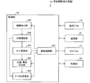
- FIG. 20 is a functional block diagram illustrating an example of a schematic configuration of the control unit 60.
- the transmission device 1b mainly includes a display panel 12 (transmission side display screen), a touch panel 14 (transmission side touch panel), a control unit 60, a communication unit 61, and a storage unit 62. Since the display panel 12 and the touch panel 14 have been described above, description thereof is omitted here.
- the shortest distance between the touch panel 14 and the outer surface B of the casing 17 may be detected when the touch panel 14 detects contact or approach of the detection target to the outer surface B. It is below the possible detectable distance (that is, a so-called narrow frame).
- the control unit 60 mainly includes a drive control unit 601 (transmission side drive control means), a mode change unit 602, and a data transmission / reception unit 603.
- the control unit 60 reads out the program stored in the storage unit 62 to a temporary recording unit (not shown) configured by, for example, a RAM (Random Access Memory) or the like, and executes the program, thereby processing the above-described members. Perform various processes.
- the drive control unit 601 controls the TP controller 33 to drive the drive line drive circuit 41 and the sense line drive circuit 42 of the touch panel 14 according to the “normal mode” or “position detection mode” determined by the mode change unit 602. To control. That is, the application control of the pulse signal for detecting the contact or approach of the detection object to the drive lines DL1 to DLn (transmission side drive line) and the drive lines DL1 to DLn and the sense line SL (transmission side sense line) Drive control for the sense line SL for detecting a change in the capacitance value of the capacitance Cf formed therebetween is performed.
- the drive control unit 601 performs drive control according to the above-described orthogonal sequence drive method (or sequential drive method) (case 1 in FIG. 21A).
- drive control application control of pulse signals to the drive lines DL1 to DLn
- the orthogonal drive system or sequential drive system
- the sense line drive circuit 42 is controlled to stop the drive control for the sense line SL by setting the sense line SL to a constant potential or high impedance (HiHZ) ((a) in FIG. 21).
- HiHZ high impedance
- drive control according to the above-described orthogonal sequence drive method may be performed as in the “normal mode”.
- the position of the transmission device 1b can be detected by the reception device 1a while the normal operation of the touch panel 14 (operation for detecting the approach or contact of the detection target) is performed.
- the drive control unit 601 supplies pulse signals (encoded pulse signals) to the drive lines DL1 to DLn in any of the operation modes
- the receiving device 1a as the counterpart device When touching or approaching, the touch panel 14 included in the receiving device 1a can receive the pulse signal.
- the position of the transmitting device 1b can be determined by the receiving device 1a.
- the mode changing unit 602 sets the operation mode of the touch panel 14 to “normal mode” in which the touch panel 14 performs a normal operation of detecting the approach or contact of the detection target, and the touch panel 14 does not perform the detection, and the partner device
- the operation mode is determined as the “position detection mode” in which position detection is performed.
- the data transmission / reception unit 603 transmits predetermined data stored in the storage unit 62 via the touch panel 14. Data transmission / reception between the touch panels 14 will be described later.
- the predetermined data transmission may be performed via the communication unit 61.
- the data transmission / reception unit 603 receives a synchronization adjustment completion notification indicating that the synchronization adjustment between the touch panels 14 has been completed or a position detection indicating that the position detection of the transmission device 1b has been completed from the receiving device 1a which is the counterpart device.
- a completion notification is received via the communication unit 61.
- the communication unit 61 transmits and receives data.
- Examples of the wireless communication used by the communication unit 61 include short-range wireless communication such as WiFi, NFC, or Bluetooth (registered trademark).
- the storage unit 62 records a control program, an application program, and the like of each unit executed by the control unit 60.
- the storage unit 62 is configured by a non-volatile recording device such as a ROM (Read Only Memory) flash memory.
- ROM Read Only Memory
- the temporary storage part mentioned above is comprised by volatile recording apparatuses, such as RAM, the memory
- storage part 62 may also be provided with the function of a temporary storage part.
- FIG. 22 is a flowchart showing the flow of processing in the transmission device 1b.
- the data transmitting / receiving unit 603 performs synchronization adjustment after the receiving device 1a, which is the counterpart device, detects the contact or approach of the transmitting device 1b, and receives a synchronization adjustment completion signal indicating that the adjustment has been completed. If the synchronization adjustment completion signal is received (YES in S2), the mode change unit 602 is notified of this.
- the mode change unit 602 switches to the “position detection mode” (S3), and the drive control unit 601 performs drive control of the touch panel 14 according to the “position detection mode”. Thereafter, the data transmission / reception unit 603 determines whether or not a position detection completion notification has been received (S4). When the position detection completion notification has been received (YES in S4), the data transmission / reception unit 603 via the communication unit 61 or the touch panel 14 Then, predetermined data is transmitted (S5).
- the touch panel 14 included in the receiving device 1a displays the above display. It is only necessary to detect the contact or approach in the region P.
- the receiving device 1a has the shortest distance between the touch panel 14 and the outer surface B of the casing 17 (receiving-side casing) such that the touch panel 14 contacts or approaches the outer surface B. It is not always necessary that the distance be less than the detectable distance (that is, a so-called narrow frame).
- the receiving device 1 a mainly includes a display panel 12 (reception side display screen), a touch panel 14 (reception side touch panel), a control unit 50, a communication unit 51, and a storage unit 52. Since the display panel 12 has been described above, a description thereof is omitted here. The basic functions of the control unit 50, the communication unit 51, and the storage unit 52 are not described because they are the same as the control unit 60, the communication unit 61, and the storage unit 62, respectively.
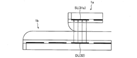
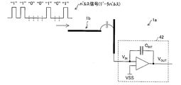
- the sense line SL of the touch panel 14 included in the receiving device 1a is applied to the drive lines DL1 to DLn of the touch panel 14 included in the transmitting device 1b that is in contact with or close to the receiving device 1a. It is possible to receive a pulse signal.
- the control unit 50 mainly includes a drive control unit 501 (reception side drive control unit), a device detection unit 502, a synchronization adjustment unit 503 (change unit), a mode change unit 504, a position / angle determination unit 505 (determination unit), and data.
- a transmission / reception unit 506 is provided.
- the drive control unit 501 controls the TP controller 33, and according to the “normal mode” or “position detection mode” determined by the mode change unit 504, the drive line drive circuit 41 of the touch panel 14 and The drive of the sense line drive circuit 42 is controlled.
- the drive control unit 501 performs drive control according to the above-described orthogonal sequence drive method (or sequential drive method) (case 2 in FIG. 21B).
- the sense line drive circuit 42 is driven in accordance with the orthogonal series drive method (or the sequential drive method), while the drive line drive circuit 41 is
- the drive lines DL1 to DLn (reception side drive lines) are set to a constant potential or high impedance (HiHZ) to control application of the pulse signals to the drive lines DL1 to DLn (FIG. 21A).
- HiHZ high impedance
- the drive control according to the above-described orthogonal sequence drive method (or sequential drive method) may be performed. Good.
- the drive control unit 501 performs the process of reading the charge (reading the output signal Vout) from the sense line SL (reception side sense line) in any of the operation modes, the transmission device 1b When touching or approaching, it is possible to determine which of the sense lines SL of the touch panel 14 included in the receiving device 1a has received the pulse signal transmitted from the touch panel 14 included in the transmitting device 1b.
- the device detection unit 502 (1) determines whether or not a coupling capacitance has occurred with any of the drive lines DL1 to DLn of the touch panel 14 included in the transmission device 1b, or (2) changes in the capacitance Cf (mutual capacitance). It is detected whether or not the transmitting device 1b as the counterpart device has come into contact or approached by determining whether or not the above has occurred.
- (1) includes, for example, a case where the touch panel 14 included in the transmission device 1b is driven. In this case, when the transmission device 1b comes into contact or approaches, the above-described coupling capacitance is generated. Therefore, the transmission device 1b is detected using a change in the output signal Vout associated with the coupling capacitance as a trigger.
- the receiving device 1a receives the pulse signal transmitted from the transmitting device 1b as mere noise.
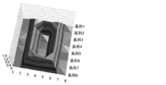
- the device detection unit 502 generates a signal distribution as shown in FIG. 23 by analyzing the output signal Vout indicating this noise. That is, when the device detection unit 502 obtains a signal distribution (noise distribution) as illustrated in FIG. 23, the device detection unit 502 can determine that the transmission device 1b has touched or approached.
- the synchronization adjustment unit 503 adjusts the synchronization between the pulse signal received from the touch panel 14 included in the transmission device 1b and the pulse signal applied to the touch panel 14 included in the reception device 1a, and synchronizes these pulse signals. It is. Accordingly, the position / angle determination unit 505 can analyze the output signal based on the pulse signal transmitted from the transmission device 1b. Details of the processing of the synchronization adjustment unit 503 will be described later.
- the mode change unit 504 determines whether the operation mode of the touch panel 14 is the “normal mode” or the “position detection mode”, similar to the mode change unit 602.
- the position / angle determination unit 505 determines which of the plurality of sense lines SL of the touch panel 14 included in the reception device 1a has received the pulse signal transmitted from the touch panel 14 included in the transmission device 1b. By doing so, the position of the transmitting device 1b with respect to the receiving device 1a is determined.
- the position / angle determination unit 505 detects a change in the capacitance value generated in the sense line SL on the receiving device 1a side by the coupling capacitance generated between the drive device DL on the transmitting device 1b side. It is determined which of the sense lines SL has received the pulse signal.
- the data transmission / reception unit 506 receives predetermined data transmitted from the transmission device 1b via the touch panel 14. The predetermined data reception may be performed via the communication unit 51. In addition, the data transmission / reception unit 506 transmits a synchronization adjustment completion notification or a position detection completion notification via the communication unit 61 to the transmission device 1b that is the counterpart device.
- FIG. 24 is a flowchart showing the flow of processing in the receiving device 1a.
- a coupling capacitance is generated between any one of the drive lines DL1 to DLn of the touch panel 14 included in the transmitting device 1b and the sense line SL of the touch panel 14 included in the receiving device 1a.
- sense line SL receives the pulse signal from the touch panel 14 with which the transmission apparatus 1b is provided (S12).
- the device detection unit 502 detects that the transmitting device 1b has come into contact or approached by grasping reception of this pulse signal (that is, reception of the output signal Vout based on this pulse signal) (S13).
- the synchronization adjustment unit 503 adjusts the synchronization of the above-described pulse signal (S14) and determines whether or not the synchronization has been achieved. (S15). If it is determined that synchronization has been established (YES in S15), the mode change unit 504 is notified of this. At this time, the data transmission / reception unit 506 is caused to transmit a synchronization adjustment completion notification to the transmission device 1b via the communication unit 51.
- the mode change unit 504 switches to the “position detection mode” (S16), and the drive control unit 501 performs drive control of the touch panel 14 in accordance with the “position detection mode” and indicates that the switch has been made. Notify the determination unit 505.
- the drive control unit 501 receives the output signal Vout based on the pulse signal supplied from the touch panel 14 included in the transmission device 1b via the sense line SL of the reception device 1a (S17)
- the drive control unit 501 indicates the position / The angle determination unit 505 is notified.
- the position / angle determination unit 505 analyzes the output signal Vout based on the received pulse signal (S18), and specifies the position (or angle) of the transmission device 1b (S19). At this time, the data transmission / reception unit 506 is caused to transmit a position detection completion notification to the transmission device 1b via the communication unit 51.
- the data transmission / reception unit 506 receives predetermined data transmitted from the transmission device 1b via the communication unit 61 or the touch panel 14 (S20). Thereby, the process according to the predetermined function currently operate
- the synchronization adjustment unit 503 described above is (1) a pulse signal applied to the drive lines DL1 to DLn of the touch panel 14 included in the transmission device 1b, received by the sense line SL of the touch panel 14 included in the reception device 1a. And (2) reception based on a correlation value (autocorrelation value) with a predetermined pattern signal (replica pattern signal) corresponding to a pulse signal applied to the drive lines DL1 to DLn of the touch panel 14 included in the receiving device 1a.
- the synchronization of the two pulse signals is adjusted by changing the application timing of the pulse signal applied to the drive line DL on the device 1a side.
- FIG. 25A is a diagram showing an equivalent circuit of the synchronization adjustment circuit 533 that generates a correlation output signal for the synchronization adjustment unit 503 to perform synchronization adjustment
- FIG. 25B is an exclusive OR circuit 533a. It is a figure which shows an example of the input-output table which is referred to.
- the synchronization adjustment circuit 533 includes an exclusive OR circuit 533a and a correlator 533b.
- this pulse signal is input to the exclusive OR circuit 533a as an input signal.
- the exclusive OR circuit 533a transmits an output signal according to the input / output table shown in FIG. 25B to the correlator 533b.
- This replica pattern signal is a signal that is synchronized with the pulse signal applied to the drive line DL on the receiving device 1a side.
- the pulse is synchronized with the change.
- the offset and / or period of the signal is also changed.
- a pseudo random pattern signal is used as the replica pattern signal. That is, the autocorrelation characteristic of the pseudo-random code is used for adjusting the two synchronizations.
- the autocorrelation characteristic of a pseudo random code is used.
- the encoded pulse signal (pseudo random pattern signal) received from the drive line DL on the transmission device 1b side is an unknown signal to the reception device 1a. That is, the pseudo random code series, code length, timing, and period of the received pulse signal are unknown.
- the replica pattern signal is changed so that the correlation output signal becomes maximum. That is, the maximum correlation value is searched by changing the pseudo random code series, code length, timing shift (offset), and period of the replica pattern signal.
- the pseudo-random code of the pulse signal received from the drive line DL on the transmission device 1b side is known.
- the pulse signal applied to the drive line DL on the transmitting device 1b side is changed. It can be synchronized with the application timing, and synchronization between both devices can be achieved.
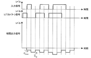
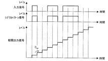
- the correlator 533b When the correlator 533b receives the output signal, the correlator 533b generates a correlation output signal indicating the correlation between the input signal and the replica pattern signal, and transmits the correlation output signal to the synchronization adjustment unit 503.
- the correlator 533b counts up when the value of the output signal shown in (b) of FIG. 25 is 0, that is, when two inputs match, and the value is 1, that is, when the two inputs do not match. Is designed to count down.
- FIG. 26 and 27 are diagrams showing an input signal, a replica pattern signal, and a correlation output signal generated by the correlator 533b.
- FIG. 26 shows a case where the two signals are not synchronized
- FIG. 27 shows a case where the two signals are synchronized.
- the synchronization adjustment unit 503 receives the correlation output signal from the correlator 533b and confirms whether the correlation value indicated by the correlation output signal is a value near 0 or the maximum value (n). It is possible to confirm whether the pulse signals applied to the drive lines DL1 to DLn of the transmission device 1b are synchronized with the pulse signals applied to the drive lines DL1 to DLn of the reception device 1a.
- the synchronization adjustment unit 503 determines that the correlation value is a value close to 0, it determines that the two pulse signals are not synchronized.
- the pulse signal applied to the drive lines DL1 to DLn on the transmission device 1b side and the pulse signal applied to the drive lines DL1 to DLn on the reception device 1a side Is determined to be synchronized.
- the synchronization adjustment unit 503 changes the offset and / or period of the replica pattern signal until the correlation value reaches the maximum value. In accordance with this change, the application timing of the pulse signal applied to the drive line DL on the receiving device 1a side is changed. Thereby, the synchronization adjustment unit 503 performs synchronization adjustment of the two pulse signals.
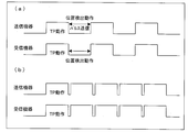
- both the transmitting device 1b and the receiving device 1a perform the position detection by switching to the “position detection mode”, as shown in FIG. 28 (a), during the normal operation (TP operation) of the touch panel 14.
- the two pulse signals are synchronized so that the position detection operation can be performed.
- the position detecting operation is also performed during the operation of the normal touch panel 14, as shown in FIG.
- the two pulse signals are synchronized.
- the receiving device 1a When the synchronization adjustment is completed, the receiving device 1a notifies the transmitting device 1b to that effect and receives basic information on the touch panel 14 from the transmitting device 1b. This information may be performed via the communication unit 61 or may be performed using data communication between the touch panels 14 described later.
- the transmitting device 1b receives a pulse signal applied to the drive lines DL1 to DLn of the touch panel 14 included in the own device when the receiving device 1a approaches or contacts the pulse signal.
- the receiving device 1a can change the application timing of the pulse signals applied to the drive lines DL1 to DLn on the receiving device 1a side.
- the information processing system 5 shown in FIG. 13 constructs a synchronization processing system including the transmission device 1b and the reception device 1a for performing the synchronization processing.
- the method of synchronizing the two pulse signals may not be based on reception of the pulse signal on the transmitting device 1b side by the receiving device 1a.
- the synchronization adjustment by the synchronization adjustment unit 503 can also be realized by receiving information from the transmission device 1b via wireless communication.
- the transmitting device 1b sends information on the pulse signal applied to the drive line DL of the own device (information including the code sequence, code length, and period used for encoding the pulse signal) to the receiving device 1a. Send.
- the receiving device 1a adjusts the application timing of the pulse signal applied to the drive line DL of the own device, thereby synchronizing with the pulse signal used on the transmitting device 1b side. .
- drive lines DL1 to DLn are collectively referred to as drive line DL.
- FIG. 29A is a schematic diagram and an equivalent circuit when the two outer surfaces B are not adjacent to each other
- FIG. 29B is a case where the two outer surfaces B are adjacent to each other. It is the figure which shows the schematic and equivalent circuit (when the outer surface B by the side of the transmission apparatus 1b contacts or approaches the outer surface B by the side of the receiving apparatus 1a).
- the description will be made on the assumption that the drive line drive circuit 41 of the transmission device 1b is in a drive state.
- FIGS. 30A and 30B are diagrams illustrating an example of a positional relationship between the transmitting device 1b and the receiving device 1a
- FIG. 30C is a diagram illustrating an example of a position detection table.
- 31 (a) and 31 (c) are schematic diagrams showing an equivalent circuit at the time of position detection.
- FIGS. 31 (b) and 31 (d) show signal distributions corresponding to (a) and (c), respectively. It is a figure which shows an example.
- the touch panel 14 included in the transmission device 1b and the reception device 1a will be described as an example in which the drive lines DL and the sense lines SL are the same number (4 ⁇ 4) and the line pitch is the same.
- pulses are applied to the drive lines DL1 to DL4 on the transmitting device 1b side according to the code sequence di as shown in FIG. A signal is applied.
- the receiving device 1a receives the pulse signal to calculate the above-described output sequence vector s4 (output signals (Vout (Y1), Vout (Y2), Vout (Y3), Vout (Y4))). , Inner product calculation di ⁇ s4 is performed.
- the position / angle determination unit 505 determines the position of the coupling capacitance generated between the drive line DL on the transmission device 1b side and the sense line SL on the reception device 1a side, and the position at that position.
- the capacity value of the binding capacity is calculated.
- the position of the coupling capacitance generated between the drive lines DL1 to DL4 and at least one of the detection electrodes SE1 to SE4 of the sense line SL1 is calculated.
- the position / angle determination unit 505 (1) is a plane having two axes, for example, the drive line DL and the sense line SL of the transmission device 1b and the drive line DL and the sense line SL of the reception device 1a.
- the capacitance value of the coupling capacitance obtained as described above and its
- a signal distribution (capacity map) as shown in (b) and (d) of FIG. 31 is generated, and the position of the transmitting apparatus 1b with respect to the receiving apparatus 1a is determined.
- the position / angle determination unit 505 includes at least one of the capacitance value generated in the sense line SL due to the coupling capacitance and the touch panel 14 on the reception device 1a side and the touch panel 14 on the transmission device 1b side where the capacitance value is generated.
- the position is specified by generating a distribution (signal distribution) of the capacitance value indicating the relationship with the position.
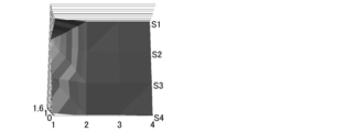
- “1” to “4” indicate positions on the sense line SL1 corresponding to the drive lines DL1 to DL4 of the transmission device 1b.
- “S1” to “S4” indicate four sense lines SL of the receiving device 1a, and “1” indicates the sense line SL1 closest to the transmitting device 1b.
- “0” to “1.6” indicate the capacitance value of the coupling capacitance obtained from each sense line SL.
- the method of taking the x-axis and the y-axis is not limited to the above.
- the x-axis and the y-axis may indicate the drive line DL and the sense line SL on the receiving device 1a side, or the transmitting device The drive line DL and the sense line SL on the 1b side may be shown.
- the position / angle determination unit 505 has a signal distribution that maximizes the capacitance value at the locations “S1” to “S4” of the sense line SL1 where the coupling capacitance is generated. Get.
- the position / angle determination unit 505 has a signal distribution in which the capacitance value becomes maximum at the locations “S1” to “S2” of the sense line SL1 where the coupling capacitance is generated. Get.
- the position / angle determination unit 505 calculates the capacitance value of the coupling capacitance obtained based on the output signal Vout and the position where the coupling capacitance is generated in the touch panel 14 included in the receiving device 1a or the transmitting device 1b. By generating a signal distribution indicating the relationship, the positional relationship of the drive line DL on the transmission device 1b side with respect to the sense line SL on the reception device 1a side is specified. As a result, the position / angle determination unit 505 can specify the position of the transmission device 1b with an accuracy finer than the line pitch unit (about 5 mm) of the drive line DL or the sense line SL.
- the position / angle determination unit 505 performs interpolation processing that is generally performed, thereby further accurately (about 0.1 mm (at least about 1/10 or less of the above-described line pitch, in units of display pixel pitch).
- the position of the transmitting device 1b can be detected.
- line identification information indicating the drive line DL may be added to the pulse signal applied to the drive line DL.
- the position / angle determination unit 505 of the receiving device 1a analyzes the line identification information, so that the outer surface B of the housing 17 corresponding to which drive line DL of the transmitting device 1b is in contact with or approaching. You may make it judge whether it is.
- the position / angle determination unit 505 calculates the capacitance value of the coupling capacitance and its position, and generates a signal distribution. it can.
- Example of position detection using position detection table In addition to detecting the position of the transmission device 1b using the signal distribution as described above, it is also possible to perform the position detection using a position detection table as shown in FIG. Hereinafter, an example of position detection using the position detection table will be described. In this example of position detection, it is assumed that the orthogonal sequence driving method is employed at least in the “normal mode”.
- FIG. 30A shows a drive line DL (d1 to d4 in the figure) on the transmission device 1b side and four detection electrodes 31a (reception side detection electrodes) that form a sense line SL1 on the reception device 1a side. ) (In the figure, SE1 to SE4) are adjacent to each other so as to face each other.
- FIG. 30 (b) shows a drive line DL (d1 to d3 in the figure) on the transmission device 1b side and three detection electrodes 31a (SE2 to SE4 in the figure) forming the sense line SL1 of the reception device 1a. ) are adjacent so as to face each other. In other words, there is no detection electrode 31a on the reception device 1a side facing the drive line DL4 on the transmission device 1b side, and there is no drive line DL on the transmission device 1b side facing the detection electrode SE1 on the reception device 1a side. State.
- the receiving device 1a when the receiving device 1a is shifted from the transmitting device 1b by one drive line DL in the upward direction on the paper surface (the direction from the drive line DL4 to DL1), in this embodiment, the receiving device 1a receives the signal from the transmitting device 1b. Assume that the amount of positional deviation from the device 1a is +1.
- the positional deviation amount when the above-mentioned deviation is made on the basis of the state of FIG. 30A is expressed as plus, and the downward direction (the direction from the drive line DL1 to DL4) in the drawing.
- the amount of misalignment in the case of misalignment is expressed as minus.
- coupling capacitances are generated between the drive lines DL1 to DL4 on the transmission device 1b side and the detection electrodes SE1 to SE4 of the sense line SL1 on the reception device 1a side.
- the inner product calculation as described above is performed, if all the capacitance values of the coupling capacitance are C, 4C is obtained as the capacitance value of the coupling capacitance when the first pulse signal is received.
- 0 is obtained as a capacitance value of the coupling capacitance when the fourth pulse signal is received.
- 3C is obtained as the capacitance value
- 1C is obtained as the capacitance value of the coupling capacitance when the second and third pulse signals are received, and the capacitance value of the coupling capacitance when the fourth pulse signal is received.
- -1C is obtained.
- the above-described output signal Vout ( Y1) to Vout (Y4) differ in how coupling capacitances corresponding to C1 to C4 are generated.
- the position detection table shown in FIG. 30C shows this predetermined specific pattern.
- a set of capacitance values corresponding to each displacement amount as shown in FIG. 30C (for example, a combination of capacitance values in the case of displacement amount “+1” (3C, 1C, 1C, ⁇ 1C) ) Each indicate the specific pattern.
- the predetermined application pattern refers to a voltage pattern for one cycle applied to each drive line DL as shown in FIG. That is, the predetermined application pattern indicates a combination of several different drive lines DL of the voltage value for one time applied simultaneously to each of the plurality of drive lines DL on the transmission device 1b side. At least the drive control unit 601 applies a pulse signal to each of the drive lines DL on the transmission device 1b side in accordance with the predetermined application pattern.
- the predetermined application pattern is obtained from the capacitance values of several drive lines DL on the transmission device 1b side, which are obtained from the coupling capacitance generated for the above-mentioned one combination. Is defined so as to coincide with any one of the predetermined number of specific patterns previously associated with the predetermined number of positional relationships of the drive line DL with respect to the sense line SL on the receiving device 1a side. I can say that.
- the position / angle determination unit 505 calculates a capacitance value obtained from each of the output signals Vout (Y1) to Vout (Y4), and compares the set of capacitance values with a specific pattern indicated by the position detection table. To do. Based on the comparison result, the position of the transmission device 1b relative to the reception device 1a (the transmission device 1b is adjacent so that the detection electrodes SE2 to SE4 of the reception device 1a face the drive lines DL1 to DL3 of the transmission device 1b). Position).
- the position / angle determination unit 505 refers to the position detection table shown in (c) of FIG. 30, so that the transmission device 1b when a coupling capacitance is generated in the sense line SL on the reception device 1a side. It is determined whether the combination of several capacitance values of the drive line DL on the side matches the combination of the capacitance values indicated by any specific pattern shown in the position detection table.
- the transmission device can be accurately transmitted in a unit smaller than the line pitch unit.
- the position of 1b can be specified. Further, the position can be detected with high accuracy in units of display pixel pitch by the interpolation processing.
- touch panels are the same shape
- the touch panels having the same shape means that at least the number of the drive lines DL and the sense lines SL of the two touch panels 14 is the same, and the line pitches of the drive lines DL and the sense lines SL are also the same.
- the touch panel 14 included in the receiving device 1a shows a case where the number of drive lines DL and sense lines SL is four, but this is only an example.
- FIG. 32 is a diagram showing the relationship between the electrode arrangement of the transmitting device 1b and the receiving device 1a and the signal distribution obtained when the contact or approach is detected.
- FIG. 32 as shown in the “image diagram”, a case where the drive line DL is shifted in the upward direction by two drive lines DL is described as an example.
- 33A to 33D show examples of equivalent circuits corresponding to cases 1 to 4 shown in FIG. 32 when the contact or approach is detected.
- FIG. 32 As the arrangement of the drive line DL on the transmission device 1b side and the sense line SL on the reception device 1a side, there are four patterns shown in FIG. 32, and the signal distribution (“output example”) as described above is obtained for each of them. It is done. Case 1 in FIG. 32 is the electrode arrangement as described in FIGS. 29 to 31, and the signal distribution is as shown in FIG. 31 (d).
- the receiving device 1a can specify a positional shift in the Y direction, and can accurately detect the position of the transmitting device 1b with respect to the receiving device 1a.
- the receiving device 1a can change the position of the transmitting device 1b. It can be detected with high accuracy.
- the size of the touch panel 14 being different means that the number of the drive lines DL and the sense lines SL of the two touch panels 14 is different, but the line pitches of the drive lines DL and the sense lines SL are the same. .
- the touch panel 14 included in the receiving device 1a shows a case where the number of drive lines DL and sense lines SL are both four.
- the touch panel 14 included in the transmission device 1b shows a case where the number of drive lines DL is eight and the number of sense lines SL is four. These numbers are merely examples.
- FIG. 34 is a diagram showing the relationship between the electrode arrangement of the transmitting device 1b and the receiving device 1a and the signal distribution obtained when the contact or approach is detected.
- the receiving device 1a is in contact with or close to the side surface of the transmitting device 1b is described as an example.
- 35A to 35D show examples of equivalent circuits corresponding to the cases 1 to 4 shown in FIG. 34 when the contact or approach is detected.
- the signal distribution has the maximum capacitance value of the coupling capacitance in “series 2” to “series 5” corresponding to the drive line DL on the transmission device 1b side.
- the receiving device 1a can specify the positional deviation in the Y direction.
- the receiving device 1b and the receiving device 1a having the electrode arrangement relationship shown in the cases 1 and 3 are used, thereby receiving the receiving device. 1a can accurately detect the position of the transmission device 1b.
- the touch panel 14 included in the receiving device 1a shows a case where the number of drive lines DL and sense lines SL is eight.
- the touch panel 14 included in the transmission device 1b shows a case where the number of drive lines DL and sense lines SL is four. These numbers are merely examples.
- FIG. 36 is a diagram showing the relationship between the electrode arrangement of the transmitting device 1b and the receiving device 1a and the signal distribution obtained when the contact or approach is detected.
- the receiving device 1a is in contact with or close to the side surface of the transmitting device 1b is described as an example.
- 37A to 37D show examples of equivalent circuits corresponding to the cases 1 to 4 shown in FIG. 36 when the contact or approach is detected.
- the signal distribution has the maximum capacitance value of the coupling capacitance in the vicinity of “series 2” to “series 5” corresponding to the sense line SL on the receiving device 1a side. .
- the receiving device 1a can specify the positional deviation in the Y direction.
- the receiving device 1b and the receiving device 1a having the electrode arrangement relationship shown in the cases 2 and 3 are used, whereby the receiving device 1a can accurately detect the position of the transmission device 1b.
- FIG. 38 is a schematic cross-sectional view of the transmission device 1b and the reception device 1a showing the state.
- an arbitrary drive line DL drive electrode 32
- a coupling capacitance is generated between the arbitrary sense line SL (detection electrode 31a).
- FIG. 39 is a diagram showing an equivalent circuit when the receiving device 1a comes into contact with or approaches the transmitting device 1b.
- FIG. 40 is a diagram showing the relationship between the electrode arrangement of the transmitting device 1b and the receiving device 1a and the signal distribution obtained when the contact or approach is detected.
- the receiving device 1a is arranged so as to overlap the center of the display area of the transmitting device 1b is described as an example.
- cases 3 and 4 shown in FIG. 40 in order to obtain an accurate signal distribution in the x direction and the y direction, two or more cases (for example, case 1 and case 2, case 2) It is preferable to measure the capacitance value of the coupling capacitance of 1 and case 4). The same applies to the “output examples” of cases 2 to 4 shown in FIG.
- 41A to 41D show examples of equivalent circuits corresponding to the cases 1 to 4 shown in FIG. 40 when the contact or approach is detected.
- the signal distribution is in the vicinity of "series 2" to “series 5" corresponding to "3" to “6” corresponding to the sense line SL on the transmission device 1b side and the drive line DL on the transmission device 1b side.
- the capacitance value of the coupling capacitance is the maximum.
- the receiving device 1a can specify a positional deviation in the Y direction in cases 1 and 3, and can specify a positional deviation in the X direction in cases 2 and 4. .
- the signal distributions are “3” to “6” corresponding to the sense line SL on the receiving device 1a side, and “series 2” to “6” corresponding to the drive line DL on the receiving device 1a side.
- the capacitance value of the coupling capacitance is the maximum.
- the receiving device 1a can specify a positional shift in the Y direction in the cases 2 and 3, and in the cases 1 and 4, the receiving device 1a can be positioned in the X direction.
- the deviation can be specified.
- the drive line DL on the transmission device 1b side and the sense line SL on the reception device 1a side are orthogonal to each other.
- the position depends on the line direction of the touch panel 14 on the large side (the touch panel 14 of the reception device 1a in FIG. 42). Detectability changes. Therefore, whether or not position detection is possible differs between cases 1 and 2 shown in FIG. 42 and cases 1 and 2 of FIG.
- FIG. 44 is a schematic cross-sectional view of the transmission device 1b and the reception device 1a showing the state.
- the detection electrodes 31a arranged along the four side surfaces receive a pulse signal from the touch panel 14 included in the transmission device 1b.
- the other detection electrodes 31 also receive the pulse signal. Therefore, the receiving device 1a can obtain a signal distribution as shown in FIG.
- FIG. 46 is a schematic cross-sectional view of the transmission device 1b and the reception device 1a showing the state.
- FIG. 47 and 48 are diagrams showing the relationship between the electrode arrangement of the transmitting device 1b and the receiving device 1a and the signal distribution obtained when the contact or approach is detected.
- FIG. 47 as shown in the “image diagram”, the side surface of the receiving device 1a comes into contact with a partial area Q1 of the display area of the transmitting device 1b, and the receiving device 1a stands on the display area of the transmitting device 1b. The case is described as an example.
- FIG. 48 as shown in the “image diagram”, the side surface of the transmission device 1b is in contact with a partial area Q2 of the display region of the reception device 1a, and the transmission device 1b is set up on the display region of the reception device 1a. It is described as an example.
- FIG. 47 there are four patterns shown in FIG. 47 as the arrangement of the drive line DL on the transmission device 1b side and the sense line SL on the reception device 1a side.
- the signal distribution is in the vicinity of “series 6” corresponding to the drive line DL on the transmission device 1b side and “3” to “6” corresponding to the sense line SL of the transmission device 1b.
- the capacitance value of the coupling capacitance is the maximum.
- the receiving device 1a can specify the positional deviation in the Y direction in the cases 1 and 3, and the positional deviation in the X direction in the cases 2 and 4. Can be identified.
- FIG. 48 there are four patterns shown in FIG. 48 as the arrangement of the drive line DL on the transmitting device 1b side and the sense line SL on the receiving device 1a side.
- the signal distribution is in the vicinity of “series 6” corresponding to the drive line DL on the receiving device 1a side and “3” to “6” corresponding to the sense line SL on the receiving device 1a side.
- the capacitance value of the coupling capacitance is the maximum.
- the receiving device 1a can specify the positional deviation in the Y direction in the cases 2 and 3, and the positional deviation in the X direction in the cases 1 and 4. Can be identified.
- the display device 1 or the like when the display device 1 or the like has the functions of both the receiving device 1a and the transmitting device 1b, the display device 1 and the like that communicate with each other have the functions of the transmitting device 1b and the receiving device 1a as needed. It is possible to replace it.
- the display device 1 and the like can mutually grasp the positions of the counterpart devices in real time. That is, the mutual position detection between the smartphones and the mutual position detection between the smartphone and the tablet can be performed in both devices in real time.
- the other device 1 or the like After the one display device 1 or the like detects the position of the counterpart device, the other device 1 or the like notifies the other device 1a and the transmission device 1b. This is realized by switching.
- FIGS. 50A to 50D show examples of equivalent circuits corresponding to the respective angles shown in the tilt detection table when contact or approach of the transmission device 1b is detected. Further, (a) to (d) of FIG. 51 are signal distributions corresponding to the respective angles.
- the position / angle determination unit 505 determines the drive line DL on the transmission device 1b side and the sense line on the reception device 1a side based on the inner product calculation result of the output sequence vector and the code sequence, as in the above-described position detection of the counterpart device. The position of the coupling capacitance generated between SL and the capacitance value of the coupling capacitance at that position is calculated. Then, the position / angle determination unit 505 generates a signal distribution as shown in FIG. 51 from the calculated capacitance value of the coupling capacitance and the position thereof, and determines the inclination of the reception device 1a with respect to the transmission device 1b.
- FIG. 50 shows a case where the number of drive lines DL and sense lines SL is four on the touch panel 14 included in the receiving device 1a.
- the touch panel 14 included in the transmission device 1b shows a case where the number of drive lines DL and sense lines SL is eight. These numbers are merely examples.
- the line pitch of each line in the touch panel 14 with which both apparatuses are provided is the same.
- FIGS. 50A to 50D correspond to the signal distributions of FIGS. 51A to 51D, respectively.
- the angles ⁇ formed between the arbitrary line segment L shown in FIG. 49A and the like and the sense line SL1 on the receiving device 1a side are 0 degrees and 41 degrees, respectively. , 60 degrees and 76 degrees are illustrated.
- “1” to “8” (x-axis in the figure) shown in the figure indicate the eight sense lines SL1 of the transmitting apparatus 1b, and “series 1” to “series 8” shown in the figure. (Y-axis in the figure) shows eight drive lines DL on the transmission device 1b side.
- the z-axis in the figure indicates the capacitance value of the coupling capacitance.
- the plane of the signal distribution (xy plane) is created based on the basic information of the touch panel 14 transmitted from the transmission device 1b after the above-described synchronization adjustment is completed.
- the position / angle determination unit 505 generates a signal distribution, thereby tilting the receiving device 1a from an arbitrary line segment L within the plane including the operation surface on the operation surface of the touch panel 14 included in the receiving device 1a ( Angle) is determined as the position of the transmission device 1b.
- the position / angle determination unit 505 is set in the operation surface of the touch panel 14 on the reception device 1a side of the reference line (sense line SL) set in the operation surface of the touch panel 14 on the transmission device 1b side.
- the angle (angle ⁇ formed) in the operation surface of the touch panel 14 on the receiving device 1a side with respect to the reference line (arbitrary line segment L) is determined.
- the angle of the transmission device 1b with respect to the reception device 1a (or the reception device 1a with respect to the transmission device 1b) can be determined. Thereby, the positional relationship with the transmission apparatus 1b can be grasped as the angle. Further, by performing the interpolation process, the angle can be specified in units of about 1 degree. That is, the angle can be detected with high accuracy.
- the position / angle determination unit 505 can perform inclination detection using the inclination detection table shown in (d) of FIG. 49 in addition to performing inclination detection using the signal distribution. An example of processing in this case will be described below.
- FIG. 49 illustrates an example in which the drive lines DL and sense lines SL of the touch panel 14 included in the transmission device 1b and the reception device 1a are the same number (4 ⁇ 4) and the line pitch is the same.
- the number is not limited to this.
- FIG. 49A shows a case where the angle ⁇ formed by an arbitrary line segment L and the sense line SL1 on the receiving device 1a side is 0 degree.
- coupling capacitance is generated between the drive lines DL1 to DL4 of the transmission device 1b and the detection electrodes SE1 to SE4 of the sense line SL1 of the reception device 1a. That is, as in the equivalent circuit of FIG. 50A, four coupling capacitors are generated on any one side of the receiving device 1a.
- FIG. 49B shows a case where the angle ⁇ formed by an arbitrary line segment L and the sense line SL1 on the receiving device 1a side is 41 degrees.
- a coupling capacitance is generated between the drive lines DL2 to DL4 of the transmission device 1b and the sense line SL1 (at least one of the detection electrodes SE1 to SE4) of the reception device 1a. Does not occur. That is, as in the equivalent circuit of FIG. 50B, three coupling capacitors are generated on any one side of the receiving device 1a.
- FIG. 49 shows a case where an angle ⁇ formed by an arbitrary line segment L and the sense line SL1 on the receiving device 1a side is 60 degrees.
- a coupling capacitance is generated between the drive lines DL3 to DL4 of the transmission device 1b and the sense line SL1 of the reception device 1a, but no coupling capacitance is generated in the portions of the drive lines DL1 and DL2. That is, as in the equivalent circuit of FIG. 50C, two coupling capacitances are generated on any one side of the receiving device 1a.
- the predetermined specific pattern is an inclination detection table shown in FIG.
- the position / angle determination unit 505 calculates the capacitance value obtained from each of the output signals Vout (Y1) to Vout (Y4), for example, similarly to the position detection, and sets the capacitance value and the inclination detection table. Is compared with the specific pattern indicated by. Then, based on the comparison result, the inclination of the receiving device 1a with respect to the transmitting device 1b is determined.
- the positional relationship with the transmission device 1b can be grasped as the angle as described above. Further, by performing the interpolation process, the angle can be specified in units of about 1 degree.
- the position of the counterpart device can be detected with an accuracy (for example, display pixel pitch unit) finer than the line pitch unit. That is, it can be said that the receiving device 1a has a configuration capable of detecting the position of the counterpart device (high-precision position detection) with high accuracy.
- the device detection unit 502 by analyzing the output signal Vout in the device detection unit 502, it is not possible to accurately detect the position as described above, but at which position the counterpart device exists with respect to the own device (for example, the own device) It is possible to perform low-accuracy position detection (low-accuracy position detection) such as existing in a partial area on one side of the device or existing on the display area side.
- low-accuracy position detection low-accuracy position detection
- position / angle determination unit 505 synchronization adjustment unit 503, mode change unit 504, position / angle determination unit 505
- FIG. 52 is a diagram illustrating an equivalent circuit when data communication is performed between the touch panels 14.
- predetermined data is transmitted from the transmitting device 1b to the receiving device 1a (S4 to S5 in FIG. 22, S19 to S20 in FIG. 24). ).
- Examples of the predetermined data include basic information (number of nodes, pitch, driving method, etc.) of the touch panel 14 included in the transmission device 1b, contents such as moving images, still images, and text data, programs (applications), functions of the transmission device 1b, There are various data such as status.
- the predetermined data includes device identification information (terminal information, device ID) for identifying the transmission device 1b and / or user identification information (user information, user ID) indicating a user who uses the transmission device 1b. ID) or the like may be included. Further, when the transmission device 1b does not have the display panel 12 (for example, a card provided with the touch panel 14), information included in the card becomes the device identification information.
- the receiving device 1a specifies in which sense line SL capacitive coupling has occurred.
- the data transmission / reception unit 506 of the receiving device 1a determines which drive line DL of the drive lines DL has capacitive coupling after the position / angle determination unit 505 performs the position detection.
- the notification is not necessarily required when the transmission device 1b itself can grasp which drive line DL has the coupling capacity, such as when the transmission device 1b has the function of the reception device 1a.
- the drive control unit 601 grasps which drive line DL has capacitive coupling, the drive control unit 601 generates a pulse signal (data pulse) on which predetermined data to be transmitted from the storage unit 62 to the reception device 1a is superimposed. Then, the pulse signal is applied to the drive line DL in which capacitive coupling occurs.
- the data transmission / reception unit 506 receives the pulse signal as the pulse signal via the sense line SL in which capacitive coupling occurs.
- the capacitive coupling is generated between the drive line DL on the transmission device 1b side and the sense line SL on the reception device 1a side, so that the touch panel 14 is used by using the pulse signal applied to the drive line DL1. Data communication between them can be realized.
- the data communication amount per unit time is larger than in the case of sequential drive. It is possible to do more. That is, when parallel driving is used, it becomes possible to perform high-speed communication compared to sequential driving.
- the coupling capacitance is added to the entire sense line SL on the receiving device 1a side as shown in FIG. Therefore, the amount of data communication can be increased as compared with the case of FIG. 13A in which the coupling capacity is generated only in some sense lines SL of the receiving device 1a.
- the drive control unit 601 of the transmission device 1b superimposes predetermined data to be transmitted to the reception device 1a on the pulse signal, and applies the data to the drive line DL of the touch panel 14 included in the own device. It can be said that it has a function of applying a pulse signal.
- the information processing system 5 shown in FIG. 13 constructs a synchronization processing system including the transmission device 1b and the reception device 1a for performing the data communication.
- Control blocks of the display devices 1, 2, and 3 (particularly, the drive control unit 501, the device detection unit 502, the synchronization adjustment unit 503, the mode change unit 504, the position / angle determination unit 505, and the data transmission / reception unit 506 provided in the reception device 1 a)
- the drive control unit 601, the mode change unit 602, and the data transmission / reception unit 603) included in the transmission device 1 b may be realized by a logic circuit (hardware) formed in an integrated circuit (IC chip) or the like, or a CPU It may be realized by software using (Central Processing Unit).
- the display device 1 or the like includes a CPU that executes instructions of a program that is software for realizing each function, and a ROM (Read Only Memory) in which the program and various data are recorded so as to be readable by the computer (or CPU).
- a storage device (these are referred to as “recording media”), a RAM (Random Access Memory) for expanding the program, and the like are provided.
- the objective of this invention is achieved when a computer (or CPU) reads the said program from the said recording medium and runs it.
- a “non-temporary tangible medium” such as a tape, a disk, a card, a semiconductor memory, a programmable logic circuit, or the like can be used.
- the program may be supplied to the computer via an arbitrary transmission medium (such as a communication network or a broadcast wave) that can transmit the program.
- a transmission medium such as a communication network or a broadcast wave
- the present invention can also be realized in the form of a data signal embedded in a carrier wave in which the program is embodied by electronic transmission.
- the electronic device which concerns on aspect 1 of this invention is an electronic device as a receiving device (receiving device 1a) provided with the receiving side touch panel (touch panel) which is a capacitive touch panel which detects the contact or approach of a target object.
- the reception side sense line (sense line SL) included in the reception side touch panel (touch panel 14) is a transmission included in the transmission side touch panel (touch panel 14) that is a capacitive touch panel provided in a transmission device that is in contact with or close to the own device.
- a pulse signal applied to the side drive line (drive line DL) can be received, and the pulse signal transmitted from the transmission side drive line can be received from a plurality of reception side sense lines included in the reception side touch panel.
- It is configured to include a signal device determination means for determining the position of the (transmission apparatus 1b) (position / angle determination unit 505).
- the pulse signal is applied by determining which reception-side sense line of the own device has received the pulse signal applied to the transmission-side drive line included in the transmission device (the pulse signal is It is possible to grasp the positional relationship between the transmission side drive line (supplied to the device itself) and the reception side sense line that has received the pulse signal.
- the position of the transmitting device with respect to the own device with an accuracy (that is, with a higher accuracy) than the distance (line pitch) between the adjacent transmitting side drive lines or receiving side sense lines.
- the position can be detected with high accuracy in units of display pixel pitch (about 0.1 mm) by interpolation processing.
- the determining means includes a capacitance generated in the receiving-side sense line due to a coupling capacitance generated between the transmitting device and the transmitting-side drive line. It is preferable to determine which of the plurality of reception-side sense lines has received the pulse signal by detecting a change in value.
- the pulse signal is applied to the transmission side drive line of the transmission side touch panel provided in the transmission device that is in contact with or close to the own device, between the transmission side drive line and the reception side sense line. Produces a coupling capacitance different from the capacitance formed on the receiving-side touch panel.
- the determining unit in the second aspect, generates a capacitance value generated in the reception-side sense line by the coupling capacitance, and a capacitance value thereof.
- a distribution signal distribution
- the capacitance value indicating a relationship with the position of at least one of the reception side touch panel and the transmission side touch panel. It is preferable to specify.
- the determining unit generates the distribution of the capacitance value, so that the coupling capacitance is generated at any position on the reception-side touch panel and / or the transmission-side touch panel. Can be grasped. Therefore, by generating the distribution of the capacitance values, it is possible to specify the positional relationship of the transmitting device with respect to the own device with a fine accuracy of a unit smaller than the line pitch, for example, a display pixel pitch unit.
- the pulse signal is the transmission of the voltage value for one time applied simultaneously to each of the plurality of transmission-side drive lines.
- the transmission drive line according to a predetermined application pattern indicating several different combinations of side drive lines the application pattern obtained from the coupling capacitance generated for the one-time combination, A pattern consisting of several capacitance values of the transmission side drive line matches one of the predetermined number of specific patterns previously associated with the predetermined number of positional relationships of the transmission side drive line with respect to the reception side sense line.
- the determining means generates the coupling capacitance in the receiving sense line. It is preferable that the positional relationship of the transmission drive line with respect to the reception sense line is specified by determining which combination of the capacitance values matches the combination of the capacitance values of the specific pattern. .
- the determination unit matches the combination of the capacitance values of the transmission side drive line when the coupling capacitance is generated in the reception side sense line and the combination of the capacitance values of any specific pattern. Is determined to identify the positional relationship.
- this specific pattern is defined by the application pattern of the pulse signal applied to the transmission drive line on the transmission device side, the pulse pattern is received from the transmission device that is in contact with or close to the own device, and By determining the match, it is possible to specify the positional relationship of the transmitting device with respect to the own device with a finer precision than a line pitch, for example, a display pixel pitch unit.
- a plurality of reception-side detection electrodes (detection electrodes 31, 31a) that respectively form the plurality of reception-side sense lines. )
- the pulse signal is preferably received by the receiving side detection electrode (detection electrode 31a) disposed along the outer edge of the receiving side touch panel.
- the pulse signal is received by the reception side detection electrode arranged along the outer edge of the reception side touch panel, at least when the side surface of the transmission device contacts or approaches the side surface of the own device (FIG. 13). (Pattern shown in (a)), the position of the transmitting device can be determined reliably.
- the device When the device is smaller than the transmitting device (when the number of receiving side drive lines or receiving side sense lines provided on the receiving side touch panel is less than the number of transmitting side drive lines or transmitting side sense lines provided on the sending side touch panel) ), It is possible to reliably determine the position of the transmitting device for other contact or approach modes (for example, the patterns shown in FIGS. 13B to 13D).
- the determining means receives the reference line set in the operation surface of the transmitting-side touch panel. It is preferable to determine an angle in the operation surface of the receiving touch panel with respect to a reference line set in the operation surface of the side touch panel.
- the angle of the transmission device with respect to the own device in the operation surface of the reception side touch panel can be determined. Thereby, the positional relationship with the transmitting device can be grasped as the angle.
- the electronic device receiving device 1a
- Aspect 7 of the present invention in any one of Aspects 1 to 6, contact of the object with respect to a receiving side drive line (drive line DL) included in the receiving side touch panel or Receiving side drive control means (drive control unit 501) for controlling the application of a pulse signal for detecting approach, and the receiving side drive control means, when the determining means determines the position of the transmitting device, It is preferable to stop the application of the pulse signal to the receiving drive line.
- the reception-side touch panel can be driven specifically for the position detection of the transmission device, and adverse effects of the position determination such as a decrease in accuracy of the position determination of the transmission device due to the object detection can be prevented.
- the electronic device (reception device 1a) in any one of aspects 1 to 7, includes a reception-side housing (housing 17) to which the reception-side touch panel is assembled.
- the shortest distance between the touch panel and the outer surface of the receiving housing is a detectable distance at which the receiving touch panel can detect contact or approach of the object to the outer surface (outer surface A or B). The following is preferable.
- the receiving side touch panel is preferably provided so as to overlap the receiving side display screen.
- the electronic device includes a transmission-side touch panel (touch panel 14) that is a capacitive touch panel that detects contact or approach of an object, and a transmission-side housing in which the transmission-side touch panel is assembled. (Housing 17), and the shortest distance between the transmission-side touch panel and the outer surface of the transmission-side housing is such that the transmission-side touch panel contacts the object with the outer surface (outer surface A or B).
- the target is an electronic device as a transmitting device (transmitting device 1b) that is equal to or shorter than a detectable distance capable of detecting an approach, and is applied to a transmitting drive line included in the transmitting touch panel.
- a receiving device capable of receiving the pulse signal approaches or contacts a pulse signal for detecting contact or approach of an object
- the reception side touch panel which is an electrostatic capacitance type touch panel in which the receiving device comprises (touch panel 14)
- the receiving apparatus comprises (touch panel 14)
- the shortest distance is equal to or less than a detectable distance capable of detecting contact or approach of an object to the outer surface of the transmission-side casing
- the shortest distance is applied to the transmission-side drive line.
- the pulse signal can be received by the receiving side touch panel provided in the receiving device. This allows the receiving device to determine which receiving-side sense line it has received, and to grasp the positional relationship between the transmitting-side drive line on the own device side and the receiving-side sense line on the receiving device side.
- the position of the own device relative to the receiving device can be determined by the receiving device with an accuracy (that is, with a higher accuracy) than the distance (line pitch) between adjacent transmission side drive lines or reception side sense lines.
- the position can be detected with high accuracy in units of display pixel pitch (about 0.1 mm) by interpolation processing.
- Transmission side drive control means for performing drive control on the transmission side sense line wherein the transmission side drive control means applies the pulse signal to each of the plurality of transmission side drive lines simultaneously.
- the transmission side drive control means applies the pulse signal to each of the plurality of transmission side drive lines simultaneously.
- the receiving device can accurately determine the position by simply applying a predetermined application pattern for detecting contact or approach of an object to each of the transmission side drive lines.
- the transmission-side drive control means further includes the above-mentioned when the position of the own device is determined by the receiving device. It is preferable to stop the drive control for the transmission-side sense line.
- the transmission-side touch panel is provided so as to overlap the transmission-side display screen.
- the image displayed on the transmission side display screen is also accurately aligned with the receiving device. It becomes possible.
- the position of the electronic device placed on the screen 215 is detected by the table-type screen device 200, and the electronic device placed on the screen 215 is detected. One of them does not detect the position of the other electronic device.
- the table-type screen device 200 is mainly considered, the table-type screen device 200 is “main”, and the electronic device placed on the screen 215 is “main”. There is a relationship.
- the “main” table type screen device 200 is indispensable, and the “main” table type screen device 200 has a special feature for recognizing the position of the “secondary” electronic device. Necessary components. Further, since it is necessary to always go through “main” during operation, a delay occurs in data communication between electronic devices that are “subordinate”.
- the receiving device receives a pulse signal applied to the transmitting drive line of the transmitting touch panel included in the transmitting device by the receiving sense line of the receiving touch panel included in the receiving device.
- a pulse signal applied to the transmitting drive line of the transmitting touch panel included in the transmitting device by the receiving sense line of the receiving touch panel included in the receiving device.
- an electronic device that functions as a receiving device functions as a transmitting device
- an electronic device that functions as a transmitting device functions as a receiving device (that is, in an electronic device that communicates with each other, By replacing the function with the receiving device), the electronic device functioning as the receiving device can grasp the position of the counterpart device in real time.
- the position of the transmitting device can be detected with high accuracy (for example, the accuracy finer than the line pitch, for example, in display pixel pitch units), it is possible to prevent erroneous recognition of the position of the transmitting device.
- the position detection can be performed without using the configuration of the “main” table type screen device 200, the position detection is performed without causing a time lag due to the “main”. be able to.
- an intuitive and easy-to-use user interface can be provided, for example, when an image is displayed on an electronic device according to an aspect of the present invention.
- the electronic device is an electronic device as a receiving device (receiving device 1a) including a receiving-side touch panel (touch panel 14) that is a capacitive touch panel that detects contact or approach of an object.
- the reception-side sense line (sense line SL) included in the reception-side touch panel is a transmission-side drive line included in the transmission-side touch panel (touch panel 14) that is a capacitive touch panel included in a transmission device that is in contact with or close to the device itself.
- the pulse signal applied to (drive line DL) can be received, and the pulse signal applied to the transmission drive line (drive line DL) received by the reception sense line and the reception touch panel are provided.
- a predetermined value corresponding to the pulse signal applied to the receiving drive line Based on the correlation value of the turn signal, a changing means for changing the application timing of the applied the pulse signal to the receiving side driveline is configured to include.
- the application timing of the pulse signal applied to the reception side drive line can be changed so as to correspond to the pulse signal applied to the transmission side drive line.
- the pulse signal received by the reception-side sense line Determining that the pulse signal applied to the receiving drive line is not synchronized, and determining that the correlation value is the maximum value, the pulse signal received by the receiving sense line; It is preferable to determine that the pulse signal applied to the receiving drive line is synchronized.
- the transmission-side touch panel touch panel 14
- the transmission-side touch panel housing 17
- the transmission-side touch panel housing 17
- the shortest distance between the transmission-side touch panel and the outer surface of the transmission-side housing is such that the transmission-side touch panel is connected to the outer surface (outer surface A or B).
- An electronic device as a transmitting device that is less than or equal to a detectable distance capable of detecting contact or approach of the object, and a transmitting drive line (drive line DL) provided in the transmitting touch panel ),
- a pulse signal for detecting contact or approach of the object is received by a receiving device that can receive the pulse signal
- the reception side touch panel touchscreen 14
- touch panel 14 which is a capacitive touch panel included in the reception device, receives the reception side, and the reception side included in the reception side touch panel by the reception device.
- the application timing of the pulse signal applied to the drive line can be changed.
- the shortest distance is equal to or less than a detectable distance capable of detecting contact or approach of an object to the outer surface of the transmission-side casing
- the shortest distance is applied to the transmission-side drive line.
- the pulse signal can be received by the receiving side touch panel provided in the receiving device.
- the application timing of the pulse signal applied to the reception side drive line can be changed so as to correspond to the pulse signal applied to the transmission side drive line of the transmission side touch panel.
- the electronic device is an electronic device as a receiving device (receiving device 1a) including a receiving-side touch panel (touch panel 14) that is a capacitive touch panel that detects contact or approach of an object.
- the reception-side sense line (sense line SL) included in the reception-side touch panel is a transmission-side touch panel (touch panel 14) that is a capacitive touch panel included in the transmission device (transmission device 1b) that is in contact with or close to the own device.
- It is the structure which receives the predetermined data superimposed on the pulse signal for detecting the contact or approach of the target object to the said transmission apparatus applied to the transmission side drive line (drive line DL) provided.
- the predetermined data superimposed on the pulse signal applied to the transmission side drive line included in the transmission side touch panel is received. Therefore, the data can be received without using a communication form for receiving the predetermined data.
- predetermined data can be received by the receiving side touch panel, the following advantages are obtained.
- -It is not necessary to visualize information to be transmitted to a receiving device, which is necessary for data communication using an optical sensor, and data communication with high security is possible.
- -No infrastructure maintenance or wireless communication required for data communication using WiFi is required. Since wireless communication is unnecessary, highly secure data communication is possible.
- -Since it is not necessary to provide a device for data communication required for data communication using WiFi or infrared rays, the electronic device can be downsized.
- the electronic device includes a transmission-side touch panel (touch panel 14) that is a capacitive touch panel that detects contact or approach of an object, and a transmission-side housing in which the transmission-side touch panel is assembled. (Housing 17), and the shortest distance between the transmission-side touch panel and the outer surface (outer surface A or B) of the transmission-side housing is such that the transmission-side touch panel contacts the object with the outer surface.
- an electronic device as a transmitting device (transmitting device 1b) that is less than a detectable distance capable of detecting an approach, and a pulse signal for detecting contact or approach of an object to the device,
- the transmitting side touch line do Transmitting-side drive control means for applying the pulse signal to Iburain DL
- drive control unit 601 is configured to include.
- the shortest distance is equal to or less than a detectable distance capable of detecting contact or approach of an object to the outer surface of the transmission-side casing, the shortest distance is applied to the transmission-side drive line.
- the pulse signal can be received by the receiving side touch panel of the receiving device.
- the transmission side drive control means superimposes predetermined data on the pulse signal, so that the reception device can receive the data via the reception side touch panel.
- An information processing system includes an electronic device (receiving device 1a) that receives the pulse signal according to any one of aspects 1 to 9, 14, 15, and 17, and aspects 10 to 13, 16 , 18, and an electronic device (transmitting device 1 b) that transmits the pulse signal.
- the electronic devices may be realized by a computer.
- the electronic device is operated by operating the computer as the means included in the electronic device.
- a control program for an electronic device that realizes the above in a computer and a computer-readable recording medium on which the control program is recorded also fall within the scope of the present invention.
- the present invention can perform processing such as position detection of a counterpart device using a capacitive touch panel, and can be used particularly for a multifunctional mobile phone, a tablet, a monitor, a television, and the like.
- Display device (electronic equipment, transmitter equipment, receiver equipment) 2 Display devices (electronic devices, transmitters, receivers) 3 Display devices (electronic devices, transmitters, receivers) 5 Information processing system 1b Transmission equipment (electronic equipment) 1a Receiving device (electronic device) 12 Display panel (reception side display screen, transmission side display screen) 14 Touch panel (reception side touch panel, transmission side touch panel, capacitive touch panel) 17 Case (Reception side case, Transmission side case) 31a Detection electrode (receiving-side detection electrode) 501 Drive control unit (reception side drive control means) 503 Synchronization adjustment unit (change means) 505 Position / angle determination unit (determination means) 601 Drive control unit (transmission side drive control means) A Outer surface B Outer surface SL Sense line (Reception side sense line, Transmission side sense line) DL drive line (receiver drive line, transmitter drive line) SL1 to SLL Sense lines (Reception side sense line, Transmission side sense line) DL
Landscapes
- Engineering & Computer Science (AREA)
- General Engineering & Computer Science (AREA)
- Theoretical Computer Science (AREA)
- Human Computer Interaction (AREA)
- Physics & Mathematics (AREA)
- General Physics & Mathematics (AREA)
- Position Input By Displaying (AREA)
- Liquid Crystal (AREA)
Abstract
Priority Applications (2)
| Application Number | Priority Date | Filing Date | Title |
|---|---|---|---|
| US14/769,474 US9727190B2 (en) | 2013-02-25 | 2014-02-13 | Electronic apparatus and information processing system |
| CN201480009863.3A CN105074634B (zh) | 2013-02-25 | 2014-02-13 | 电子设备和信息处理系统 |
Applications Claiming Priority (2)
| Application Number | Priority Date | Filing Date | Title |
|---|---|---|---|
| JP2013034995 | 2013-02-25 | ||
| JP2013-034995 | 2013-02-25 |
Publications (1)
| Publication Number | Publication Date |
|---|---|
| WO2014129375A1 true WO2014129375A1 (fr) | 2014-08-28 |
Family
ID=51391170
Family Applications (1)
| Application Number | Title | Priority Date | Filing Date |
|---|---|---|---|
| PCT/JP2014/053302 Ceased WO2014129375A1 (fr) | 2013-02-25 | 2014-02-13 | Appareil électronique et système de traitement d'informations |
Country Status (3)
| Country | Link |
|---|---|
| US (1) | US9727190B2 (fr) |
| CN (1) | CN105074634B (fr) |
| WO (1) | WO2014129375A1 (fr) |
Cited By (1)
| Publication number | Priority date | Publication date | Assignee | Title |
|---|---|---|---|---|
| CN105528975A (zh) * | 2014-10-15 | 2016-04-27 | 精工爱普生株式会社 | 驱动器以及电子设备 |
Families Citing this family (2)
| Publication number | Priority date | Publication date | Assignee | Title |
|---|---|---|---|---|
| US9658728B2 (en) * | 2013-06-20 | 2017-05-23 | Sharp Kabushiki Kaisha | Touch panel controller, integrated circuit, touch panel device, and electronic device |
| KR102489956B1 (ko) * | 2015-12-30 | 2023-01-17 | 엘지디스플레이 주식회사 | 표시 장치 및 표시 장치의 구동 방법 |
Citations (5)
| Publication number | Priority date | Publication date | Assignee | Title |
|---|---|---|---|---|
| JP2000020231A (ja) * | 1997-01-08 | 2000-01-21 | Alan Woodfield David | 位置情報を得るための装置 |
| JP2009253478A (ja) * | 2008-04-02 | 2009-10-29 | Sony Ericsson Mobilecommunications Japan Inc | 情報通信装置、情報通信装置の制御方法 |
| JP2011242966A (ja) * | 2010-05-18 | 2011-12-01 | Nec Corp | タッチセンサ、タッチパネルおよび該タッチセンサを用いた情報伝達方法 |
| WO2011155939A1 (fr) * | 2010-06-10 | 2011-12-15 | Empire Technology Development Llc | Communication entre dispositifs à panneau tactile |
| WO2012026567A1 (fr) * | 2010-08-27 | 2012-03-01 | 京セラ株式会社 | Dispositif terminal portatif |
Family Cites Families (11)
| Publication number | Priority date | Publication date | Assignee | Title |
|---|---|---|---|---|
| US6452514B1 (en) | 1999-01-26 | 2002-09-17 | Harald Philipp | Capacitive sensor and array |
| US8269746B2 (en) * | 2006-11-27 | 2012-09-18 | Microsoft Corporation | Communication with a touch screen |
| US20090128513A1 (en) * | 2007-11-20 | 2009-05-21 | Samsung Electronics Co., Ltd | Device identification method and apparatus, device information provision method and apparatus, and computer-readable recording mediums having recorded thereon programs for executing the device identification method and the device information provision method |
| US9405444B2 (en) * | 2010-10-01 | 2016-08-02 | Z124 | User interface with independent drawer control |
| JP4927216B1 (ja) | 2010-11-12 | 2012-05-09 | シャープ株式会社 | 線形素子列値推定方法、静電容量検出方法、集積回路、タッチセンサシステム、及び電子機器 |
| JP5657471B2 (ja) | 2011-05-30 | 2015-01-21 | オリンパスイメージング株式会社 | デジタルプラットフォーム装置 |
| US9086883B2 (en) * | 2011-06-10 | 2015-07-21 | Qualcomm Incorporated | System and apparatus for consolidated dynamic frequency/voltage control |
| US9041687B2 (en) * | 2011-12-07 | 2015-05-26 | Htc Corporation | Communication method for capacitive touch panel |
| CN105519229A (zh) * | 2013-12-30 | 2016-04-20 | 联发科技股份有限公司 | 触控通信连接建立方法及触控面板装置 |
| KR20160045269A (ko) * | 2014-10-17 | 2016-04-27 | 엘지전자 주식회사 | 웨어러블 디바이스 및 상기 디바이스와 통신 가능한 이동 단말기 |
| KR20160047273A (ko) * | 2014-10-22 | 2016-05-02 | 엘지전자 주식회사 | 와치 타입 단말기 |
-
2014
- 2014-02-13 CN CN201480009863.3A patent/CN105074634B/zh not_active Expired - Fee Related
- 2014-02-13 US US14/769,474 patent/US9727190B2/en not_active Expired - Fee Related
- 2014-02-13 WO PCT/JP2014/053302 patent/WO2014129375A1/fr not_active Ceased
Patent Citations (5)
| Publication number | Priority date | Publication date | Assignee | Title |
|---|---|---|---|---|
| JP2000020231A (ja) * | 1997-01-08 | 2000-01-21 | Alan Woodfield David | 位置情報を得るための装置 |
| JP2009253478A (ja) * | 2008-04-02 | 2009-10-29 | Sony Ericsson Mobilecommunications Japan Inc | 情報通信装置、情報通信装置の制御方法 |
| JP2011242966A (ja) * | 2010-05-18 | 2011-12-01 | Nec Corp | タッチセンサ、タッチパネルおよび該タッチセンサを用いた情報伝達方法 |
| WO2011155939A1 (fr) * | 2010-06-10 | 2011-12-15 | Empire Technology Development Llc | Communication entre dispositifs à panneau tactile |
| WO2012026567A1 (fr) * | 2010-08-27 | 2012-03-01 | 京セラ株式会社 | Dispositif terminal portatif |
Cited By (1)
| Publication number | Priority date | Publication date | Assignee | Title |
|---|---|---|---|---|
| CN105528975A (zh) * | 2014-10-15 | 2016-04-27 | 精工爱普生株式会社 | 驱动器以及电子设备 |
Also Published As
| Publication number | Publication date |
|---|---|
| US20150378478A1 (en) | 2015-12-31 |
| CN105074634A (zh) | 2015-11-18 |
| US9727190B2 (en) | 2017-08-08 |
| CN105074634B (zh) | 2018-01-26 |
Similar Documents
| Publication | Publication Date | Title |
|---|---|---|
| JP6990673B2 (ja) | 静電容量感知デバイスのための多重センサタッチ統合表示ドライバ構成 | |
| US10564775B2 (en) | Method and apparatus for improved input sensing using a display processor reference signal | |
| JP6484227B2 (ja) | 静電容量感知デバイスのための多重センサタッチ統合表示ドライバ構成 | |
| US10007828B2 (en) | Fingerprint sensor integrated type touch screen device | |
| CN105074633B (zh) | 输入设备和显示装置 | |
| US9329731B2 (en) | Routing trace compensation | |
| US9772701B2 (en) | Touch detection device, and display device with touch detection function and electronic apparatus including the same | |
| CN107045394B (zh) | 输入装置、处理系统以及电容感测方法 | |
| KR20170030735A (ko) | 지문센서 일체형 표시장치 및 그를 구동하는 방법과 장치 | |
| US11474635B2 (en) | Display noise filter for a sensing device | |
| JP2015133105A (ja) | 一体型入力装置における電極干渉の軽減 | |
| CN105468215B (zh) | 用于电容感测的电流反馈技术 | |
| US9335843B2 (en) | Display device having touch sensors and touch data processing method thereof | |
| KR102299421B1 (ko) | 터치패널 표시 장치, 능동형 스타일러스 펜 및 그 제어방법 | |
| US9268435B2 (en) | Single layer capacitive sensor and capacitive sensing input device | |
| CN105074634B (zh) | 电子设备和信息处理系统 | |
| US10401671B2 (en) | Liquid crystal panel having touch sensor function | |
| KR102481784B1 (ko) | 지문센서 일체형 터치 스크린 장치와 그 구동방법 | |
| US9459367B2 (en) | Capacitive sensor driving technique that enables hybrid sensing or equalization |
Legal Events
| Date | Code | Title | Description |
|---|---|---|---|
| WWE | Wipo information: entry into national phase |
Ref document number: 201480009863.3 Country of ref document: CN |
|
| 121 | Ep: the epo has been informed by wipo that ep was designated in this application |
Ref document number: 14754593 Country of ref document: EP Kind code of ref document: A1 |
|
| WWE | Wipo information: entry into national phase |
Ref document number: 14769474 Country of ref document: US |
|
| NENP | Non-entry into the national phase |
Ref country code: DE |
|
| 122 | Ep: pct application non-entry in european phase |
Ref document number: 14754593 Country of ref document: EP Kind code of ref document: A1 |
|
| NENP | Non-entry into the national phase |
Ref country code: JP |