WO2014132803A1 - 電力用半導体装置 - Google Patents
電力用半導体装置 Download PDFInfo
- Publication number
- WO2014132803A1 WO2014132803A1 PCT/JP2014/053287 JP2014053287W WO2014132803A1 WO 2014132803 A1 WO2014132803 A1 WO 2014132803A1 JP 2014053287 W JP2014053287 W JP 2014053287W WO 2014132803 A1 WO2014132803 A1 WO 2014132803A1
- Authority
- WO
- WIPO (PCT)
- Prior art keywords
- power semiconductor
- semiconductor device
- press
- fit
- constricted
- Prior art date
- Legal status (The legal status is an assumption and is not a legal conclusion. Google has not performed a legal analysis and makes no representation as to the accuracy of the status listed.)
- Ceased
Links
Images


Classifications
-
- H—ELECTRICITY
- H10—SEMICONDUCTOR DEVICES; ELECTRIC SOLID-STATE DEVICES NOT OTHERWISE PROVIDED FOR
- H10W—GENERIC PACKAGES, INTERCONNECTIONS, CONNECTORS OR OTHER CONSTRUCTIONAL DETAILS OF DEVICES COVERED BY CLASS H10
- H10W76/00—Containers; Fillings or auxiliary members therefor; Seals
- H10W76/10—Containers or parts thereof
- H10W76/12—Containers or parts thereof characterised by their shape
- H10W76/15—Containers comprising an insulating or insulated base
-
- H—ELECTRICITY
- H01—ELECTRIC ELEMENTS
- H01R—ELECTRICALLY-CONDUCTIVE CONNECTIONS; STRUCTURAL ASSOCIATIONS OF A PLURALITY OF MUTUALLY-INSULATED ELECTRICAL CONNECTING ELEMENTS; COUPLING DEVICES; CURRENT COLLECTORS
- H01R12/00—Structural associations of a plurality of mutually-insulated electrical connecting elements, specially adapted for printed circuits, e.g. printed circuit boards [PCB], flat or ribbon cables, or like generally planar structures, e.g. terminal strips, terminal blocks; Coupling devices specially adapted for printed circuits, flat or ribbon cables, or like generally planar structures; Terminals specially adapted for contact with, or insertion into, printed circuits, flat or ribbon cables, or like generally planar structures
- H01R12/50—Fixed connections
- H01R12/51—Fixed connections for rigid printed circuits or like structures
- H01R12/55—Fixed connections for rigid printed circuits or like structures characterised by the terminals
- H01R12/58—Fixed connections for rigid printed circuits or like structures characterised by the terminals terminals for insertion into holes
- H01R12/585—Terminals having a press fit or a compliant portion and a shank passing through a hole in the printed circuit board
-
- H—ELECTRICITY
- H01—ELECTRIC ELEMENTS
- H01R—ELECTRICALLY-CONDUCTIVE CONNECTIONS; STRUCTURAL ASSOCIATIONS OF A PLURALITY OF MUTUALLY-INSULATED ELECTRICAL CONNECTING ELEMENTS; COUPLING DEVICES; CURRENT COLLECTORS
- H01R13/00—Details of coupling devices of the kinds covered by groups H01R12/70 or H01R24/00 - H01R33/00
- H01R13/02—Contact members
- H01R13/04—Pins or blades for co-operation with sockets
- H01R13/05—Resilient pins or blades
-
- H—ELECTRICITY
- H01—ELECTRIC ELEMENTS
- H01R—ELECTRICALLY-CONDUCTIVE CONNECTIONS; STRUCTURAL ASSOCIATIONS OF A PLURALITY OF MUTUALLY-INSULATED ELECTRICAL CONNECTING ELEMENTS; COUPLING DEVICES; CURRENT COLLECTORS
- H01R13/00—Details of coupling devices of the kinds covered by groups H01R12/70 or H01R24/00 - H01R33/00
- H01R13/40—Securing contact members in or to a base or case; Insulating of contact members
- H01R13/405—Securing in non-demountable manner, e.g. moulding, riveting
-
- H—ELECTRICITY
- H01—ELECTRIC ELEMENTS
- H01R—ELECTRICALLY-CONDUCTIVE CONNECTIONS; STRUCTURAL ASSOCIATIONS OF A PLURALITY OF MUTUALLY-INSULATED ELECTRICAL CONNECTING ELEMENTS; COUPLING DEVICES; CURRENT COLLECTORS
- H01R4/00—Electrically-conductive connections between two or more conductive members in direct contact, i.e. touching one another; Means for effecting or maintaining such contact; Electrically-conductive connections having two or more spaced connecting locations for conductors and using contact members penetrating insulation
- H01R4/28—Clamped connections, spring connections
- H01R4/48—Clamped connections, spring connections utilising a spring, clip, or other resilient member
-
- H—ELECTRICITY
- H10—SEMICONDUCTOR DEVICES; ELECTRIC SOLID-STATE DEVICES NOT OTHERWISE PROVIDED FOR
- H10W—GENERIC PACKAGES, INTERCONNECTIONS, CONNECTORS OR OTHER CONSTRUCTIONAL DETAILS OF DEVICES COVERED BY CLASS H10
- H10W72/00—Interconnections or connectors in packages
- H10W72/50—Bond wires
-
- H—ELECTRICITY
- H10—SEMICONDUCTOR DEVICES; ELECTRIC SOLID-STATE DEVICES NOT OTHERWISE PROVIDED FOR
- H10W—GENERIC PACKAGES, INTERCONNECTIONS, CONNECTORS OR OTHER CONSTRUCTIONAL DETAILS OF DEVICES COVERED BY CLASS H10
- H10W76/00—Containers; Fillings or auxiliary members therefor; Seals
- H10W76/40—Fillings or auxiliary members in containers, e.g. centering rings
- H10W76/42—Fillings
- H10W76/47—Solid or gel fillings
-
- H—ELECTRICITY
- H10—SEMICONDUCTOR DEVICES; ELECTRIC SOLID-STATE DEVICES NOT OTHERWISE PROVIDED FOR
- H10W—GENERIC PACKAGES, INTERCONNECTIONS, CONNECTORS OR OTHER CONSTRUCTIONAL DETAILS OF DEVICES COVERED BY CLASS H10
- H10W90/00—Package configurations
-
- H—ELECTRICITY
- H10—SEMICONDUCTOR DEVICES; ELECTRIC SOLID-STATE DEVICES NOT OTHERWISE PROVIDED FOR
- H10W—GENERIC PACKAGES, INTERCONNECTIONS, CONNECTORS OR OTHER CONSTRUCTIONAL DETAILS OF DEVICES COVERED BY CLASS H10
- H10W42/00—Arrangements for protection of devices
- H10W42/121—Arrangements for protection of devices protecting against mechanical damage
-
- H—ELECTRICITY
- H10—SEMICONDUCTOR DEVICES; ELECTRIC SOLID-STATE DEVICES NOT OTHERWISE PROVIDED FOR
- H10W—GENERIC PACKAGES, INTERCONNECTIONS, CONNECTORS OR OTHER CONSTRUCTIONAL DETAILS OF DEVICES COVERED BY CLASS H10
- H10W72/00—Interconnections or connectors in packages
- H10W72/071—Connecting or disconnecting
- H10W72/075—Connecting or disconnecting of bond wires
- H10W72/07541—Controlling the environment, e.g. atmosphere composition or temperature
- H10W72/07554—Controlling the environment, e.g. atmosphere composition or temperature changes in dispositions
-
- H—ELECTRICITY
- H10—SEMICONDUCTOR DEVICES; ELECTRIC SOLID-STATE DEVICES NOT OTHERWISE PROVIDED FOR
- H10W—GENERIC PACKAGES, INTERCONNECTIONS, CONNECTORS OR OTHER CONSTRUCTIONAL DETAILS OF DEVICES COVERED BY CLASS H10
- H10W72/00—Interconnections or connectors in packages
- H10W72/50—Bond wires
- H10W72/541—Dispositions of bond wires
- H10W72/5445—Dispositions of bond wires being orthogonal to a side surface of the chip, e.g. parallel arrangements
-
- H—ELECTRICITY
- H10—SEMICONDUCTOR DEVICES; ELECTRIC SOLID-STATE DEVICES NOT OTHERWISE PROVIDED FOR
- H10W—GENERIC PACKAGES, INTERCONNECTIONS, CONNECTORS OR OTHER CONSTRUCTIONAL DETAILS OF DEVICES COVERED BY CLASS H10
- H10W72/00—Interconnections or connectors in packages
- H10W72/50—Bond wires
- H10W72/551—Materials of bond wires
- H10W72/552—Materials of bond wires comprising metals or metalloids, e.g. silver
- H10W72/5524—Materials of bond wires comprising metals or metalloids, e.g. silver comprising aluminium [Al]
-
- H—ELECTRICITY
- H10—SEMICONDUCTOR DEVICES; ELECTRIC SOLID-STATE DEVICES NOT OTHERWISE PROVIDED FOR
- H10W—GENERIC PACKAGES, INTERCONNECTIONS, CONNECTORS OR OTHER CONSTRUCTIONAL DETAILS OF DEVICES COVERED BY CLASS H10
- H10W72/00—Interconnections or connectors in packages
- H10W72/851—Dispositions of multiple connectors or interconnections
- H10W72/874—On different surfaces
- H10W72/884—Die-attach connectors and bond wires
-
- H—ELECTRICITY
- H10—SEMICONDUCTOR DEVICES; ELECTRIC SOLID-STATE DEVICES NOT OTHERWISE PROVIDED FOR
- H10W—GENERIC PACKAGES, INTERCONNECTIONS, CONNECTORS OR OTHER CONSTRUCTIONAL DETAILS OF DEVICES COVERED BY CLASS H10
- H10W74/00—Encapsulations, e.g. protective coatings
-
- H—ELECTRICITY
- H10—SEMICONDUCTOR DEVICES; ELECTRIC SOLID-STATE DEVICES NOT OTHERWISE PROVIDED FOR
- H10W—GENERIC PACKAGES, INTERCONNECTIONS, CONNECTORS OR OTHER CONSTRUCTIONAL DETAILS OF DEVICES COVERED BY CLASS H10
- H10W90/00—Package configurations
- H10W90/701—Package configurations characterised by the relative positions of pads or connectors relative to package parts
- H10W90/751—Package configurations characterised by the relative positions of pads or connectors relative to package parts of bond wires
- H10W90/753—Package configurations characterised by the relative positions of pads or connectors relative to package parts of bond wires between laterally-adjacent chips
-
- H—ELECTRICITY
- H10—SEMICONDUCTOR DEVICES; ELECTRIC SOLID-STATE DEVICES NOT OTHERWISE PROVIDED FOR
- H10W—GENERIC PACKAGES, INTERCONNECTIONS, CONNECTORS OR OTHER CONSTRUCTIONAL DETAILS OF DEVICES COVERED BY CLASS H10
- H10W90/00—Package configurations
- H10W90/701—Package configurations characterised by the relative positions of pads or connectors relative to package parts
- H10W90/751—Package configurations characterised by the relative positions of pads or connectors relative to package parts of bond wires
- H10W90/754—Package configurations characterised by the relative positions of pads or connectors relative to package parts of bond wires between a chip and a stacked insulating package substrate, interposer or RDL
Definitions
- the present invention relates to a power semiconductor device, and more particularly to a structure of a terminal for connection to another device.
- SiC silicon carbide
- the semiconductor device a plurality of terminals are arranged so as to protrude from the housing (see, for example, Patent Document 1). And since the connection part corresponding to the terminal of the semiconductor device is arrange
- a press-fit terminal in which a bent portion having a bent shape is formed on a leg portion in order to follow the above-described arrangement error (see, for example, Patent Document 2).
- the bent portion is buckled and deformed earlier than the elastic portion (press fit portion) when the press fit is inserted. Therefore, at the time of press-fit insertion, it is necessary to support the pressed surface provided in a portion closer to the elastic portion than the bent portion, and there is a problem that it is difficult to insert the press-fit terminal into the through hole.
- the present invention has been made to solve the above-described problems, and an object thereof is to obtain a highly reliable power semiconductor device that can be easily incorporated into a connected device.
- the power semiconductor device of the present invention includes a housing, a circuit board provided in the housing and formed with an electrical circuit including the power semiconductor element, and an internal terminal electrically connected to the electrical circuit in the housing.
- a body, an external terminal portion for electrical connection with a connected device, and one end connected to the internal terminal portion is fixed in the housing, and the other end supports the external terminal portion so as to be separated from the housing
- a plurality of terminals, each of the plurality of terminals is a portion of the body portion exposed from the housing, and a base portion of the external terminal portion and a portion exposed from the housing
- a constricted portion constricted from both sides in a direction perpendicular to the center line is formed so as to leave a center line portion connecting the two.
- the constricted portion having low rigidity can be deformed preferentially over the external terminal portion, so that the stress can be suppressed. Therefore, a highly reliable power semiconductor device can be obtained.
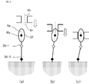
- FIG. 2 is a plan view and a front view for explaining the configuration of the power semiconductor device according to the first embodiment of the present invention. It is sectional drawing for demonstrating the structure of the semiconductor device for electric power concerning Embodiment 1 of this invention. It is sectional drawing for demonstrating the integration state to the apparatus of the power semiconductor device concerning Embodiment 1 of this invention. It is the partial side view which permeate
- FIG. 1 to 6 are diagrams for explaining the configuration of the power semiconductor device according to the first embodiment of the present invention.
- FIGS. 1 (a) and 1 (b) show the appearance of the power semiconductor device, respectively.
- FIG. 2 is a cross-sectional view corresponding to the line AA in FIG. 1A
- FIG. 3 is a cross-sectional view of FIG. 4 is a cross-sectional view corresponding to the line BB
- FIG. 4 is a partial side view through which a case portion is transmitted for explaining the state of the terminal in the power semiconductor device
- FIG. 5 is a front view for explaining the configuration of the terminal.
- FIG. 6 is a side view, FIG.
- FIG. 6 is a combination of a front view and a cross-sectional view (a) of the frame (part) of the terminal, which is the base of the terminal, for explaining the terminal processing step, It is a combination figure (b) of a front view and a side view.
- FIG. 7 is a cross-sectional view for explaining the configuration of the power semiconductor device according to the modification, and the drawing reference is the same as FIG. Details will be described below.
- the power semiconductor device 1 is entirely covered with a package 2 (insert case 21 and lid 22) with the base plate 4 exposed from the lower surface side, and the insert case 21 constituting the package 2 2), a mounting hole 2h for mounting a heat sink for heat dissipation to the base plate 4 is formed.
- a plurality of press-fit terminals 3 serving as terminals are arranged on the upper surface portion of the power semiconductor device 1 so as to protrude from the package 2 in order to ensure electrical connection with the outside (device to be connected). Yes.
- the power semiconductor device 1 is provided with a circuit board 5 in which a plurality of patterns 52 made of copper are formed on the circuit surface (upper side in the drawing) side of the ceramic base 51 in the package 2. Yes.
- a copper base plate 4 is joined to the heat radiating surface (lower side in the figure) of the circuit board 5 by solder 8.
- One of the circuit surface patterns 52 is an IGBT (Insulated Gate) using silicon as a semiconductor material.
- Bipolar transistor (61) and FwDi (free-wheeling diode) 62 (collectively power semiconductor element 6) are joined by solder 8.
- a plurality of aluminum wires 7 having a diameter of 200 to 400 ⁇ m are wire-bonded to the upper electrodes of the IGBT 61 and the FwDi 62, and the wires formed on the other pattern 52 and the portion of the press-fit terminal 3 in the package 2. It is connected to the bond part 35.
- the inside of the insert case 21 is sealed with a silicon gel 23 and is packaged by covering the opened upper portion with a lid 22.
- the press-fit terminal 3 protruding from the upper surface of the package 2 has a predetermined position on a plane perpendicular to the insertion direction to the connected device as shown in FIG. Is arranged. Furthermore, as will be described in the manufacturing method described later, the configuration is such that those arranged in a straight line along the width direction of the terminals are arranged. Then, at the time of incorporation into the connected device, as shown in FIG. 3, the press-fit portion 32 that is a contact point with the outside of the press-fit terminal 3 is a contact point on the connected device (printed board 9 in the figure) side. Insert into the through hole 9h.
- the inner wall of the through-hole 9h is covered with a conductor electrically connected to the plurality of patterns 92 formed on the circuit surface of the printed circuit board 9 by copper plating, and comes into contact with the inserted press-fit portion 32, Electrical connection (conduction) with the power semiconductor device 1 is ensured.
- a press-fit portion 32 is formed at one end of the press-fit terminal 3 as a contact that is inserted into the above-described printed board 9 and is electrically connected to the through hole 9 h.
- a wire bond portion 35 is formed for wire bonding to a circuit member such as the pattern 52 in the semiconductor device 1 or the power semiconductor element 6.
- it has the body part 33 which connects the press fit part 32 and the wire bond part 35, and the part (insert part 33u) and the wire bond part 35 by the side of the wire bond part 35 among the body parts 33 are semiconductors for electric power.
- the body part 33 supports the press fit part 32 so as to be separated from the package 2.
- the surface of the press-fit portion 32 and the exposed portion 33e is plated with nickel base tin commonly used for electrical contacts, and the wire bond portion 35 is subjected to bright nickel plating so that aluminum wire bonding is possible.
- the size of the press-fit terminal 3 is such that the body portion 33 has a width Wm of 3 mm, a plate thickness t of 1 mm, and the press-fit portion 32 has a maximum width Wp of 2.1 mm.
- the press fit portion 32 has a needle eye shape so as to have a spring property in order to ensure contact with the inner wall of the through hole 9h.
- a doubly-supported beam in which an opening is formed between a pair of branch portions that branch out from a tapered tip that is the tip in the terminal press-fitting direction in a direction perpendicular to the press-fitting direction and the plate thickness direction ( width direction) It has a structure, and the width Wb of each branch portion is 0.7 mm.
- the cross-sectional shape of the press-fit portion 32 follows the shape (cylindrical shape) of the inner wall of the through hole 9h, and R processing (R0.3) is applied to the corners of the four corners so as to increase the contact area.
- the specification of the through-hole 9h of the printed circuit board 9 is that the plating thickness is 25 to 50 ⁇ m and the finished diameter is 2.0 mm inside diameter, which is slightly smaller than the maximum width Wp (2.1 mm) of the press-fit portion 32. ing.
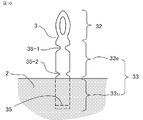
- a constricted portion 36 that is recessed from both sides in the width direction. Is formed.
- the concave shape from both sides for forming the constricted portion 36 is bilaterally symmetric, and the opening length (height in the drawing) Hc and the depth are the same.
- the constricted portion 36 of the press-fit terminal 3 used in the power semiconductor device 1 according to the first embodiment has an opening length Hc of 1 mm and a depth of 1.2 mm, and the tip prevents local stress concentration. R0.5 processing is applied.
- the (remaining meat) width Wc of the constricted portion 36 is 0.6 mm (Wm ⁇ 1.2 mm ⁇ 2), which is narrower than the width Wb (0.7 mm) of the branch portion.
- the press-fit terminal 3 is manufactured from a metal plate material having a thickness of 1 mm, and a terminal unit 3P as a base of the press-fit terminal 3 is a tie bar as shown in FIG. 6A by press working using a plurality of progressive dies. It is formed from a frame 30 connected at 38. In the frame 30 in a state where the terminal units 3P are connected, the region A32 corresponding to the press-fit portion 32 and the exposed portion 33e is subjected to lower layer nickel plating and upper layer tin plating of about several ⁇ m thickness, The area A35 corresponding to the portion 35 is subjected to bright nickel plating. After that, as shown in FIG. 6B, in order to form a wire bond pad (wire bond portion 35), it is bent at the LB portion while being connected (integrated) by a tie bar 38.
- the frame 30 is inserted into the insert mold in a state where the predetermined number of terminal units 3P are connected by the tie bars 38, and the frame 30 is embedded by injection molding so that the press-fit portion 32 and the wire bond portion 35 are exposed.
- the insert case 21 is molded.
- the terminal units 3P are connected (integrated) by the tie bars 38, so that the insertion into the insert mold is facilitated.
- the tie bar 38 is separated, and the insert case 21 in which the press-fit terminals 3 are arranged at predetermined positions is completed.
- the base plate 4 to which the power semiconductor element 6 and the like are soldered and the insert case 21 are bonded with an adhesive, and the circuit members such as the power semiconductor element 6 and the pattern 52 and the wire bond portion 35 of the press-fit terminal 3 are bonded. Are connected by wire bonding. Finally, the circuit surface is sealed with silicon gel 23, and the lid 22 is bonded to form a package, whereby the power semiconductor device 1 is completed.
- the power semiconductor device 1 is used by being attached to a device such as a printed circuit board 9 provided with a contact corresponding to the press-fit terminal 3.
- the power semiconductor device 1 and the printed circuit board 9 are exposed to a severe environment such as temperature change and vibration during use.
- the linear expansion coefficient of the printed circuit board 9 about 13 ppm / K
- the linear expansion coefficient of the power semiconductor device the line of the package 2). Due to the difference in expansion coefficient (about 5 ppm / K), repeated displacement occurs between the arrangement of the press-fit terminals 3 of the power semiconductor device 1 and the arrangement of the contacts of the printed circuit board 9.
- the copper cylinder used for the terminal needs to be thickened according to the current density. Since the rigidity increases as the thickness increases, a load is repeatedly applied to the contacts of the printed circuit board 9 or the power semiconductor device 1 when displacement occurs. For this reason, it has been difficult to apply to larger power semiconductor devices and in more severe environments.
- the portion exposed from the package 2 (exposed portion 33e)
- a constricted portion 36 having a width Wc narrower than the width Wb of the branch portion of the press-fit portion 32 was formed. Therefore, even if such repeated displacement occurs, the constricted portion 36 is preferentially deformed, and the press-fit portion 32 moves to the left and right in the width direction of the terminal with the constricted portion 36 as the center.
- the load applied to the semiconductor device 1 can be suppressed. That is, it is possible to provide the power semiconductor device 1 with high reliability.
- a press-fit terminal 3 that is slightly wider than the diameter of the through-hole 9h of the printed circuit board 9 is press-fitted, and the press-fit connection is mechanically performed between the press-fit portion 32 and the through-hole 9h.
- This is a technology that generates contact force and electrically connects the two. Therefore, when there is a relative displacement between the through-hole 9h and the press-fit terminal 3, only one of the branch portions forming the press-fit portion 32 hits the inner wall of the through-hole 9h at the start of insertion, resulting in plastic deformation and spring property. Is damaged and the contact force becomes difficult to work. Therefore, a high positional accuracy is required for the arrangement of the through holes 9h of the printed circuit board 9 that is a contact point of the connected device.
- the constricted portion 36 is deformed to absorb the relative positional deviation. Further, it is possible to suppress the occurrence of excessive plastic deformation in the press fit portion 32. As a result, the power semiconductor device 1 can be easily incorporated into the printed circuit board 9.
- the above-described effect can be obtained when the rigidity of the constricted portion 36 is smaller than the rigidity of the press-fit portion 32 with respect to the stress in the direction perpendicular to the insertion direction. Specifically, it can be obtained when the width Wc of the constricted portion 36 is smaller than the width Wb on one side of the branch portion, which is the representative width of the press-fit portion 32. That is, when the width Wc of the constricted portion 36 is wider than the width Wb on one side of the branch portion constituting the press-fit portion 32, if the misalignment occurs between the printed circuit board 9 and the press-fit portion 32, the constricted portion 36 is Before the plastic deformation, the press fit portion 32 is largely plastic deformed. Therefore, the spring property in the press fit part 32 is impaired, and the contact cannot secure predetermined electrical characteristics.
- the present invention is not limited to this.
- the solder contact 32V as shown in FIG. 7 uses a pin terminal 3V formed in a flat plate shape for soldering, the rigidity of the constricted portion 36 is smaller than the rigidity of the solder contact 32V. A form may be realized.
- a constricted portion 36 having a width Wc narrower than the representative width of the solder contact 32V (here, the width of a simple flat plate portion) is provided.
- a crack may occur in the soldered portion due to a difference in linear expansion coefficient between the power semiconductor device 1 and the printed circuit board 9 due to a temperature change when the power semiconductor device 1 is used.
- the recess 36 absorbs the stress due to the difference in linear expansion coefficient, the stress applied to the contact portion and the power semiconductor device 1 is reduced, and the reliability is increased.
- the pin terminal 3V may be soldered to the printed circuit board 9 by a soldering iron. At that time, heat escapes to the power semiconductor device 1 side with respect to heat input from the soldering iron. The heat input time must be lengthened. In response to this problem, the constricted portion 36 prevents heat from escaping, so that the heat input time can be shortened.
- the constricted portion 36 can be formed by punching, and a punching pattern (frame 30 in the present embodiment) that is the source of the terminal. Can be processed at the same time as molding. Therefore, the cost increase for forming the constricted part 36 hardly occurs.
- the terminal material may be a copper-based material, and the electrical resistivity is particularly close to oxygen-free copper. Moreover, when an appropriate repulsive force is required like the press-fit terminal 3, it is preferable that it is a highly rigid material with high rigidity.
- a copper-zinc alloy (conductivity 80%, elastic modulus 140 GPa) exists as a material satisfying these characteristics.
- the insert case type power semiconductor device 1 sealed with the silicon gel 23 has been described as an example.
- the transfer mold type power semiconductor device entirely covered with the mold resin Can exhibit the same effect.
- the dimensions of the terminal (press-fit terminal 3) and the through hole 9h may be different from those described above, and the connection method between the terminal and the contact on the connected device side may be in another form.
- the width Wc of the constricted portion 36 is narrower than at least the representative width of the terminal (in this embodiment, the width Wb on one side of the branch portion of the press-fit portion 32 and the width of the pin terminal 3V). Good.
- the end portion on the side arranged in the package 2 does not necessarily need to be the wire bond portion 35, and may be a press fit shape or a pin terminal shape. Also in this case, the same effect can be achieved by forming the above-described constricted portion 36 in a portion that is not supported by the package 2 like the exposed portion 33e.
- the housing (package 2) and the electricity installed in the housing (package 2) and including the power semiconductor element 6 are included.
- the circuit board 5 on which the circuit is formed, the internal terminal part (wire bond part 35) electrically connected to the electric circuit in the housing (package 2), and the connected device (for example, the printed board 9) are electrically connected.
- External terminal portion (press-fit portion 32 or solder contact 32V) and one end (insert portion 33u) connected to the internal terminal portion (wire bond portion 35) are fixed in the housing (package 2) and the other end
- Terminal 3 or pin terminal 3V) and each of a plurality of terminals (press-fit terminal 3 or pin terminal 3V) is exposed to a portion (exposed portion 33e) of body portion 33 exposed from the casing.
- the constricted portion 36 having a rigidity lower than the rigidity of the external terminal portion (the press-fit portion 32 or the solder contact 32V) is formed, even if a displacement or an arrangement error due to a temperature change occurs. Since the constricted part 36 is deformed preferentially, the press-fit part 32 or the solder contact 32V moves to the left and right in the width direction of the terminal with the constricted part 36 as the center. Such a load can be suppressed. That is, it is possible to provide the power semiconductor device 1 with high reliability.
- the terminals are each formed of a long plate material, and the portions where the external terminal portions (press-fit portions 32) branch in the width direction of the plate materials are opposed to each other with a gap therebetween. Since it is formed in a double-supported beam structure and the width Wc of the constricted portion 36 is configured to be narrower than the respective width Wb of the branched portion of the external terminal portion (press fit portion 32), the constricted portion 36 is deformed. Since the relative displacement is absorbed, it is possible to suppress the occurrence of excessive plastic deformation in the press fit portion 32. As a result, the electrical connection at the contacts is good, and the incorporation of the power semiconductor device 1 into the printed circuit board 9 becomes easy.
- FIG. 8 is a diagram for explaining the configuration of the power semiconductor device according to the second embodiment, and FIG. 8A is a partial side view in which a case portion is allowed to pass through in order to explain the state of a terminal.
- FIG. 8B is a partial plan view when viewed from the viewpoint C in FIG. 8A, for explaining a state between adjacent terminals. Since the other basic configuration of the power semiconductor device is the same as that of the power semiconductor device of the first embodiment, the description thereof is omitted.
- the press-fit terminal 3 that is a terminal is formed with a constricted portion 36 similar to that of the first embodiment.
- a part of the constricted portion 36 is a package 2. It hangs on the insert part 33u embedded inside.
- the press-fit portion 32 side is twisted (rotated) 45 degrees about the center in the width direction and the thickness direction with the narrow portion 36 (strictly in the vicinity of the central portion of the narrow portion) as a boundary, and is arranged with respect to the insert portion 33u. It is designed to tilt with respect to the direction.
- this structure can be realized by bending the portion exposed from the insert case 21 after the injection molding of the insert case 21 described in the first embodiment. For example, it is difficult to use the frame 30 in which the processing in the twisting direction is applied to each terminal unit 3P for injection molding because of the mold configuration.
- a terminal of a plate material such as the press-fit terminal 3 has a dimension in the width direction (the same Wm) larger than a dimension in the thickness direction (for example, t in FIG. 5). Therefore, if the press-fit terminals 3 are arranged and the pitch is to be narrowed while keeping the interval between the adjacent press-fit terminals 3, the press-fit terminals 3 may be arranged in the plate thickness direction.
- the press-fit terminals 3 are arranged in a direction parallel to the surface so as not to overlap in the thickness direction of the plate material.
- the press-fit terminals 3 are necessarily arranged in a line along the width direction.
- the surface exposed from the package 2 is inclined with respect to the arrangement direction after the insert molding.
- the arrangement pitch can be reduced while keeping the distance Dp between the adjacent press-fit terminals 3 in the portion exposed from the package 2 at a predetermined value or more.
- the interval Du of the insert portion 33u is shortened, but since the package 2 is made of an insulating material, it may be a spatial distance shorter than the spatial distance required for the exposed portion.
- the inclination is not limited to 45 degrees, and may be set as appropriate at an angle of 90 degrees or greater and greater than 0 degrees, but an angle satisfying Dp ⁇ Dc is preferable.
- the terminals are each formed of a long plate material and the casing of the body portion 33.
- the portion (exposed portion 33e) that is disposed along the width direction of the plate material in the portion (insert portion 33u) fixed in the body (package 2) and that is exposed from the housing (package 2), it is ahead of the constricted portion 36. Since the portion on the side of the press-fit portion 32 or the solder contact 32V is inclined with respect to the width direction, the terminal (the press-fit terminal 3 or the pin terminal 3V) is maintained while maintaining a narrow pitch. Thus, it is possible to provide a small and high withstand voltage power semiconductor device.
- each of the terminals is configured so that a part of the constricted portion 36 is embedded in the housing (package 2), and thus is not surrounded by an insulating material. The space distance of the part can be secured firmly.
- the temperature of the power semiconductor device 1 as a whole is further increased, and a connected device such as the printed circuit board 9. Therefore, the stress relaxation effect by the constricted portion 36 becomes remarkable.
- the terminals also become hot, so if the contact points between the terminals and the connected device are soldered, the solder joint reliability is reduced. There was something to do.
- the current flowing through the terminals is also large, the amount of heat generated at the contact portion is increased, and the solder joint reliability is sometimes lowered.
- the power semiconductor element can be operated at a temperature higher than the melting point of the solder.
- the press-fit portion 32 has a smaller electrode connection area than soldering (for example, the solder contact 32V of the pin terminal 3V), the thermal resistance between the press-fit portion 32 and the through hole 9h is increased. Therefore, if the press-fit terminal 3 is used as a terminal, heat conduction from the power semiconductor device 1 to the printed circuit board 9 can be suppressed, and the heat of the power semiconductor element 6 is not easily transmitted to the connected device (printed circuit board 9) side. Become. That is, even if the temperature of the power semiconductor device 1 becomes high, the temperature of the connected device is hardly increased, and the reliability of the connected device is increased.
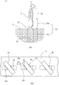
- FIG. 9A and 9B are views for explaining a method of attaching the device according to the third embodiment, and are cross-sectional views showing states at respective steps in the method of attaching the power semiconductor device and the printed circuit board, respectively.
- the cutting position is the same as in FIG.
- the attachment method of the apparatus concerning this Embodiment 3 is an attachment method using the characteristic of the power semiconductor device 1 using the press fit terminal 3 demonstrated in Embodiment 1 and 2.
- the other configurations are the same as those described in the first or second embodiment, and thus description thereof is omitted.
- the power semiconductor device itself is the one shown in FIGS. 1 to 6 described in the first embodiment, but the one shown in FIG. 8 described in the second embodiment is also applicable. Needless to say.
- the power semiconductor device 1 when the printed circuit board 9 is attached to the power semiconductor device 1, the power semiconductor device 1 is placed under a press machine (not shown) so that the press-fit terminals 3 that are external terminals face upward. It is mounted at a predetermined position of the lower jig 201 installed in the mold. At that time, for example, the power semiconductor device 1 is positioned by the pin 201p provided in the lower jig 201 and the mounting hole 2h. Then, the printed board 9 is temporarily mounted on the upper surface of the press-fit terminal 3 with the positions of the press-fit terminals 3 (arrangement thereof) and the through holes 9 h (arrangement thereof) aligned.
- the upper jig 202 installed on the upper mold of the press machine (not shown) is moved toward the lower jig 201.
- the upper jig 202 is provided with a gap 202h in a portion corresponding to the through hole 9h. Therefore, even if the tip of the press-fit terminal 3 passes through the through-hole 9h and protrudes from the printed board 9, it does not touch the pressing surface of the upper jig 202, so the printed board 9 is pushed down to a necessary position. (Press).
- the press fit part 32 of each press fit terminal 3 can be inserted to the predetermined position of the through hole 9h, and the attachment of the power semiconductor device 1 and the printed circuit board 9 is completed.
- the constriction is formed only from one side of the body portion, it can be bent only in the direction in which the constriction is present, and it is difficult to follow depending on the misalignment direction of the terminal and the through hole. . Further, when the constriction from one side is formed so that the material of the central axis does not exist, the force is applied in the vertical direction (insertion direction) and the constriction is inclined in the constricted direction. In that case, for example, like the press-fit terminal described in Patent Document 2, unless the press-fit portions themselves are individually supported, insertion into the through hole becomes difficult.
- the power semiconductor device has a large number of terminals and various terminal arrangements, and it is extremely difficult to produce a jig that supports or presses a plurality of terminals.
- the structure like the bent portion disclosed in Patent Document 2 is not suitable for energizing a large current because a long and narrow current path is formed and the electric resistance is increased.
- the constricted portion 36 is formed from both ends in the width direction so that the body portion 33 of the press-fit terminal 3 remains in the center in the width direction.
- the constricted portion 36 does not buckle and the portion where the current path becomes narrow is limited.
- the constricted portion 36 can be easily deformed in both the left and right directions in the width direction which is a direction perpendicular to the insertion direction. As a result, the power semiconductor device 1 can be normally attached to the printed circuit board 9 with high productivity.
- the body part 33 has the same position and width in the length direction so that the material remains at the center in the width direction.
- the constricted portion 36 is formed from both ends in the direction.
- a constriction is formed so that there is a remaining portion on both sides of the center line (center axis of the body portion 33) connecting the press fit portion 32 and the base of the exposed portion 33e, that is, the center axis in the insertion direction. It only has to be. In this case, for example, it is not always necessary to be bilaterally symmetric, and for example, a form that can be bundled from both sides in the thickness direction may be employed.
- FIG. 10 to 12 are diagrams for explaining the configuration of a power semiconductor device according to a modification of the third embodiment, and FIG. 10 is a diagram for explaining the state of a press-fit terminal in the power semiconductor device.
- FIG. 11 is a front view and a side view for explaining the configuration of a press-fit terminal, and FIG. 12 is an illustration of inserting a terminal into a through hole when a printed circuit board is attached to a power semiconductor device. It is a schematic diagram which shows the deformation
- the press-fit terminal 3 used in the power semiconductor device 1 according to the present modification includes the constricted portions 36-1 at different positions (two locations) in the length direction (insertion direction) of the exposed portion 33e. 36-2 is formed.
- each of the constricted portions 36-1 and 36-2 satisfies the above-described condition that there is a remaining portion on both sides of the central axis.
- the two narrowed portions 36-1 and 36-2 are arranged such that the width Wc2 of the narrowed portion 36-2 farther from the press-fit portion 32 is closer to the closer (36-1). It was formed to be wider than the width Wc1.
- the distance between the center portion Pp of the press-fit portion 32 and the constricted portion 36-1 (center position Pc1) in the length direction is less than the distance Lpc between the constricted portion 36-1 and the constricted portion 36-2 (center position Pc2).
- the distance Lcc is formed to be longer.
- the center axis Xp of the press-fit terminal 3 and the center axis Xh of the through hole 9h are displaced in parallel in the direction perpendicular to the insertion direction, and the through hole 9h is pressed in this state. Lower toward the fit terminal 3.
- the press fit part 32 is induced
- the constricted portion 36-2 farthest from the press-fit portion 32 is bent first.
- the press fit portion 32 enters the through hole 9h, so that the inclination is corrected along the inner wall of the through hole 9h.
- the width Wc1 of the constricted portion 36-1 is narrower than the width Wc-2 of the constricted portion 36-2, the constricted portion 36-1 can be easily deformed.
- the direction of 9h can be matched.
- the two constricted portions 36-1 and 36-2 are provided at different positions in the length direction. And the inclination of the press fit portion 32 can be made to follow the through hole 9h.
- the width Wc1 of the constricted portion 36-1 closer to the press fit portion 32 is made smaller than the width Wc2 of the constricted portion 36-2 farther away, the inclination of the press fit portion 32 in the latter half of the insertion is easy. Can be corrected.
- the distance Lcc between the constricted portion 36-1 and the constricted portion 36-2 is longer than the distance Lpc between the press fit portion 32 (center position Pp) and the constricted portion 36-1, the insertion is performed.
- the press fit portion 32 can be tilted so as to be easily guided to the through hole 9h.
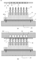
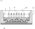
- FIG. 13 is a cross-sectional view corresponding to FIG. 2 in the second embodiment and transmits a built-in printed board portion through the power semiconductor device according to the fourth embodiment of the present invention.
- the power semiconductor device is generally called an intelligent power module incorporating a power device drive circuit and a self-protection function circuit.
- the intelligent power module includes a control board 9I in which a drive circuit and the like are incorporated in a package 2V of the power semiconductor device 1V. That is, the control board 9I is disposed at a position deeper than the upper surface of the package 2V.
- the through hole 9h of the control board 9I is temporarily inserted into the tip of each press-fit terminal 3. Then, the space between the bottom surface (base plate side) of the power semiconductor device 1V and the top surface of the control board 9I is pressed to insert each press-fit terminal 3 into the through hole 9h at one time, and the insertion is completed.
- the pressed surface of the press-fit terminal is gripped with a jig as in Patent Document 2, for example. It is impossible to insert it. Therefore, in the case of a press-fit terminal having a portion (bent part) where no material exists on the central axis of the body part, the bent part is buckled and the press-fit terminal is not inserted. Furthermore, when the remaining thickness is biased to one side of the central axis, the deformation direction is limited, and it can only cope with a positional shift in one direction.
- the body portion 33 is not buckled because the body portion 33 is formed with the constriction 36 so that there is a remaining wall on both sides of the central axis in the insertion direction. For this reason, even when mounting is performed in the internal space 2Vs as in the fourth embodiment, it is not necessary to support the body portion 33 of each press-fit terminal 3, and can be inserted into the through hole 9h. Is possible. Since it is not necessary to support the trunk
Landscapes
- Coupling Device And Connection With Printed Circuit (AREA)
- Chemical & Material Sciences (AREA)
- Dispersion Chemistry (AREA)
- Power Conversion In General (AREA)
- Inverter Devices (AREA)
Abstract
Description
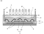
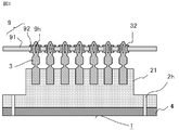
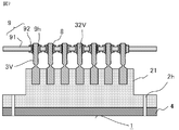
図1~図6は本発明の実施の形態1にかかる電力用半導体装置の構成を説明するためのものであり、図1(a)と図1(b)はそれぞれ電力用半導体装置の外観を示す平面図と正面図、図2は図1(a)のA-A線に対応する断面図、図3は電力用半導体装置の機器への組み込み状態を説明するための図1(a)のB-B線に対応する断面図、図4は電力用半導体装置中での端子の状態を説明するためにケース部分を透過させた部分側面図、図5は端子の構成を説明するための正面図と側面図、図6は端子の加工工程を説明するための、端子の元となるフレーム(一部)の曲げ工程前の正面図と断面図の組合せ図(a)と、曲げ加工後の正面図と側面図の組合せ図(b)である。また、図7は変形例にかかる電力用半導体装置の構成を説明するための断面図で、描画基準は図3と同様である。以下、詳細に説明する。
図1に示すように、電力用半導体装置1は、ベース板4が下面側から露出した状態で全体がパッケージ2(インサートケース21と蓋22)により覆われ、パッケージ2(を構成するインサートケース21)には、放熱用のヒートシンクをベース板4に取り付けるための取り付け穴2hが形成されている。一方、電力用半導体装置1の上面部には、外部(被接続機器)との電気接続を確保するために、端子である複数のプレスフィット端子3が、パッケージ2から突出するように配置されている。
図2に示すように、電力用半導体装置1には、パッケージ2内にセラミック基材51の回路面(図中上側)側に銅による複数のパターン52が形成された回路基板5が設置されている。回路基板5の放熱面(図中下側)には、はんだ8によって銅製のベース板4が接合され、回路面のパターン52のうちのひとつには、半導体材料にシリコンを用いたIGBT(Insulated Gate Bipolar Transistor)61とFwDi(Free-Wheeling Diode)62(まとめて電力用半導体素子6)がはんだ8で接合されている。IGBT61、FwDi62の上部電極には、直径200~400μmのアルミニウムのワイヤ7が、複数本ワイヤボンディングされており、他のパターン52上や、プレスフィット端子3のパッケージ2内の部分に形成されたワイヤボンド部35に接続されている。なお、インサートケース21の内部はシリコンゲル23にて封止され、開放された上部を蓋22で覆うことでパッケージ化される。
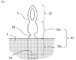
プレスフィット端子3の一端には、図4に示すように、例えば、上述したプリント基板9に挿入してスルーホール9hと導通させる接点となるプレスフィット部32が形成され、他端には、電力用半導体装置1内のパターン52あるいは電力用半導体素子6等の回路部材とのワイヤボンドを行うためのワイヤボンド部35が形成されている。そして、プレスフィット部32と、ワイヤボンド部35とをつなぐ胴体部33とを有し、胴体部33のうち、ワイヤボンド部35側の部分(インサート部33u)とワイヤボンド部35が電力用半導体装置1のパッケージ2内に埋め込まれ、胴体部33の残りの部分(露出部33e)がプレスフィット部32をパッケージ2から引き離すように支持している。プレスフィット部32および露出部33eの表面には、電気接点に一般的に用いられるニッケル下地スズめっきが施され、ワイヤボンド部35にはアルミワイヤボンディングが可能なように、光沢ニッケルめっきが施される。
プレスフィット端子3は、厚さ1mmの金属板材から製作され、複数の順送型を用いたプレス加工により図6(a)に示すように、プレスフィット端子3の元となる端子ユニット3Pがタイバー38で連結されたフレーム30から形成される。フレーム30は、各端子ユニット3Pが連結された状態で、プレスフィット部32および露出部33eに対応する領域A32には、厚さ数μm程度の下層ニッケルめっきおよび上層スズめっきが施され、ワイヤボンド部35に対応する領域A35には光沢ニッケルメッキが施される。その後、図6(b)に示すように、ワイヤボンドパッド(ワイヤボンド部35)を形成するためにタイバー38で連結(一体化)されたままの状態で、LB部分で折り曲げ加工される。
図3で説明したように、電力用半導体装置1はプレスフィット端子3に対応した接点が設けられたプリント基板9のような機器に取り付けられて使用される。ここで、電力用半導体装置1とプリント基板9は使用中に温度変化や振動などの苛酷な環境にさらされる。使用中の温度変化により、電力用半導体装置1はこれらの環境にさらされた際に、プリント基板9の線膨張係数(約13ppm/K)と電力用半導体装置の線膨張係数(パッケージ2の線膨張係数:約5ppm/K)の違いにより、電力用半導体装置1のプレスフィット端子3の配列とプリント基板9の接点の配列間に繰り返し変位が生じる。
なお、本実施の形態では、端子として、上述した効果が顕著に顕れるプレスフィット端子3を用いた場合について説明したが、これに限ることはない。例えば、図7に示すようなはんだ用接点32Vがはんだ付け用の平板状に形成されたピン端子3Vを用いた場合でも、はんだ用接点32Vの剛性よりも、括れ部36の剛性の方が小さい形態を実現すればよい。
本実施の形態2にかかる電力用半導体装置は、実施の形態1で説明した電力用半導体装置に対して、端子の括れ部の一部をケース内に埋め込むようにするとともに、括れ部分から上を捻るようにしたものである。図8は本実施の形態2にかかる電力用半導体装置の構成を説明するためのもので、図8(a)は、端子の状態を説明するためにケース部分を透過させた部分側面図、図8(b)は、隣接する端子間の状態を説明するためのもので、図8(a)の視点Cから見たときの部分平面図である。その他の電力用半導体装置としての基本的な構成については、実施の形態1の電力用半導体装置と同じであるので説明を省略する。
プレスフィット端子3のような板材の端子は、厚み方向の寸法(例えば図5のt)よりも幅方向の寸法(同Wm)の方が大きい。そのため、プレスフィット端子3を配列し、隣接するプレスフィット端子3の間隔を保ったまま、ピッチを狭めようとすれば、各プレスフィット端子3を極端に言えば板厚方向に並べればよい。
本実施の形態3では、上述した実施の形態1および2で説明した電力用半導体装置とプリント基板とを接続する方法(機器の取付方法)について説明する。そして、接続する際に括れ部の構造に起因するプレスフィット端子の動作について説明する。図9(a)と(b)は本実施の形態3にかかる機器の取付方法を説明するためのもので、それぞれ電力用半導体装置とプリント基板との取付方法における工程ごとの状態を示す断面図であり、切断位置は図2と同様である。
本実施の形態4にかかる電力用半導体装置は、上述した各実施の形態で説明したプレスフィット端子を備えたものであるが、パッケージとの位置関係が異なるものである。図13は、本発明の実施の形態4にかかる電力用半導体装置を説明するためのもので、実施の形態2における図2に対応する断面図であるとともに、内蔵するプリント基板部分を透過させた図である。
2Vs:内部空間、3:プレスフィット端子(端子)、
3V:ピン端子(端子)、4:ベース板、5:回路基板、
6:電力用半導体素子、7:ボンディングワイヤ、8:はんだ、
9:プリント基板(被接合機器)、 9h:スルーホール(接点)、
9I:制御基板(被接合機器)、32:プレスフィット部(外部端子部)、
32V:はんだ用接点(外部端子部)、33:胴体部、33e:露出部、
33u:インサート部、35:ワイヤボンド部(内部端子部)、
36:括れ部、36-1:プレスフィット部に近い方の括れ部、
36-2:プレスフィット部から遠い方の括れ部、201:下治具、
202:上治具、Lcc:括れ部間の距離、
Lcp:プレスフィット部の中心と近い方の括れ部との距離、
Pp:プレスフィット部の長方向の中心、
Wb:プレスフィット部の分岐部のそれぞれの幅、
Wc:括れ部の幅、 Wc1:近い方の括れ部の幅、
Wc2:遠い方の括れ部の幅。
Claims (10)
- 筐体と、
前記筐体内に設置され、電力用半導体素子を含む電気回路が形成された回路基板と、
前記筐体内で前記電気回路と電気接続される内部端子部と、被接続機器と電気接続するための外部端子部と、前記内部端子部に連なる一端が前記筐体内で固定され、他端で前記外部端子部を前記筐体から引き離すように支持する胴体部とを有する複数の端子と、を備え、
前記複数の端子のそれぞれは、前記胴体部のうち、前記筐体から露出した部分に、前記外部端子部と前記筐体から露出した部分の根元部分とを結ぶ中心線の部分を残すように、前記中心線に垂直な方向における両側から括れた括れ部が形成されていることを特徴とする電力用半導体装置。 - 前記複数の端子は、それぞれ長尺状の板材で形成されているとともに、
前記括れ部は、前記板材の幅方向における両側から括れていることを特徴とする請求項1に記載の電力用半導体装置。 - 前記複数の端子は、それぞれ前記外部端子部が前記幅方向に分岐した部分のそれぞれが間隔を隔てて対向する両持梁構造に形成され、
前記括れ部の幅が、前記外部端子部の分岐した部分のそれぞれの幅よりも狭いことを特徴とする請求項2に記載の電力用半導体装置。 - 前記複数の端子は、それぞれ前記胴体部の前記筐体内で固定された部分における前記板材の幅方向に沿って配置され、
前記筐体から露出した部分のうち、前記括れ部より先の部分が、前記幅方向に対して傾いていることを特徴とする請求項2または3に記載の電力用半導体装置。 - 前記複数の端子のそれぞれは、前記括れ部の一部が前記筐体内に埋め込まれていることを特徴とする請求項4に記載の電力用半導体装置。
- 前記複数の端子のそれぞれには、前記括れ部が前記中心線に沿った異なる位置に複数形成されていることを特徴とする請求項1から5のいずれか1項に記載の電力用半導体装置。
- 前記複数形成された括れ部のうち、前記外部端子部に近い方の括れ部の幅よりも、遠い方の括れ部の幅の方が広いことを特徴とする請求項6に記載の電力用半導体装置。
- 前記複数の端子のそれぞれの前記外部端子部が、前記筐体の内部で配列されていることを特徴とする請求項1から7のいずれか1項に記載の電力用半導体装置。
- 前記電力用半導体素子がワイドバンドギャップ半導体材料により形成されていることを特徴とする請求項1から8のいずれか1項に記載の電力用半導体装置。
- 前記ワイドバンドギャップ半導体材料は、炭化ケイ素、窒化ガリウム系材料、およびダイヤモンドのうちのいずれかであることを特徴とする請求項9に記載の電力用半導体装置。
Priority Applications (6)
| Application Number | Priority Date | Filing Date | Title |
|---|---|---|---|
| CN201480009806.5A CN105074919B (zh) | 2013-02-26 | 2014-02-13 | 电力用半导体装置 |
| KR1020157023029A KR101728264B1 (ko) | 2013-02-26 | 2014-02-13 | 전력용 반도체 장치 |
| EP14757420.6A EP2963684B1 (en) | 2013-02-26 | 2014-02-13 | Power semiconductor device |
| JP2015502853A JP6157584B2 (ja) | 2013-02-26 | 2014-02-13 | 電力用半導体装置組み込み機器の製造方法および電力用半導体装置 |
| US14/655,962 US9640453B2 (en) | 2013-02-26 | 2014-02-13 | Power semiconductor device |
| US15/463,134 US9887142B2 (en) | 2013-02-26 | 2017-03-20 | Power semiconductor device |
Applications Claiming Priority (2)
| Application Number | Priority Date | Filing Date | Title |
|---|---|---|---|
| JP2013-035291 | 2013-02-26 | ||
| JP2013035291 | 2013-02-26 |
Related Child Applications (2)
| Application Number | Title | Priority Date | Filing Date |
|---|---|---|---|
| US14/655,962 A-371-Of-International US9640453B2 (en) | 2013-02-26 | 2014-02-13 | Power semiconductor device |
| US15/463,134 Continuation US9887142B2 (en) | 2013-02-26 | 2017-03-20 | Power semiconductor device |
Publications (1)
| Publication Number | Publication Date |
|---|---|
| WO2014132803A1 true WO2014132803A1 (ja) | 2014-09-04 |
Family
ID=51428075
Family Applications (1)
| Application Number | Title | Priority Date | Filing Date |
|---|---|---|---|
| PCT/JP2014/053287 Ceased WO2014132803A1 (ja) | 2013-02-26 | 2014-02-13 | 電力用半導体装置 |
Country Status (6)
| Country | Link |
|---|---|
| US (2) | US9640453B2 (ja) |
| EP (1) | EP2963684B1 (ja) |
| JP (2) | JP6157584B2 (ja) |
| KR (1) | KR101728264B1 (ja) |
| CN (1) | CN105074919B (ja) |
| WO (1) | WO2014132803A1 (ja) |
Cited By (10)
| Publication number | Priority date | Publication date | Assignee | Title |
|---|---|---|---|---|
| CN106252292A (zh) * | 2015-06-15 | 2016-12-21 | 三菱电机株式会社 | 压接端子、半导体装置、电力变换装置及压接端子的制造方法 |
| JP2016219778A (ja) * | 2015-05-15 | 2016-12-22 | 三菱電機株式会社 | 電力用半導体装置 |
| US9979105B2 (en) | 2015-05-15 | 2018-05-22 | Mitsubishi Electric Corporation | Power semiconductor device |
| JP2019012716A (ja) * | 2017-06-29 | 2019-01-24 | タイコエレクトロニクスジャパン合同会社 | 印刷回路基板 |
| JP2020017702A (ja) * | 2018-07-27 | 2020-01-30 | 富士電機株式会社 | 半導体装置 |
| JP2021072329A (ja) * | 2019-10-30 | 2021-05-06 | 三菱電機株式会社 | パワー半導体装置 |
| CN113130404A (zh) * | 2021-04-02 | 2021-07-16 | 深圳市嘉兴南电科技有限公司 | 一种电动汽车车载5g天线用三极管 |
| WO2025192191A1 (ja) * | 2024-03-11 | 2025-09-18 | ローム株式会社 | 半導体装置、電力変換ユニットおよび車両 |
| WO2025253837A1 (ja) * | 2024-06-07 | 2025-12-11 | 富士電機株式会社 | 半導体装置 |
| WO2026014297A1 (ja) * | 2024-07-09 | 2026-01-15 | 株式会社オートネットワーク技術研究所 | プレスフィット端子 |
Families Citing this family (15)
| Publication number | Priority date | Publication date | Assignee | Title |
|---|---|---|---|---|
| DE102015115122B4 (de) * | 2015-09-09 | 2022-05-19 | Infineon Technologies Ag | Leistungshalbleitermodul mit zweiteiligem Gehäuse |
| JP6870531B2 (ja) * | 2017-08-21 | 2021-05-12 | 三菱電機株式会社 | パワーモジュールおよび電力変換装置 |
| JP6806024B2 (ja) * | 2017-10-03 | 2020-12-23 | 三菱電機株式会社 | 半導体装置 |
| JP7070658B2 (ja) * | 2018-03-16 | 2022-05-18 | 富士電機株式会社 | 半導体装置 |
| JP6989824B2 (ja) * | 2018-03-29 | 2022-01-12 | 株式会社アテックス | 端子、端子を備えたパワーモジュール用射出成形体、及びその製造方法 |
| CN109727947B (zh) | 2018-11-19 | 2020-12-15 | 华为技术有限公司 | 一种引脚、引脚组合结构、封装体及其制作方法 |
| US11682606B2 (en) * | 2019-02-07 | 2023-06-20 | Ford Global Technologies, Llc | Semiconductor with integrated electrically conductive cooling channels |
| JP7257900B2 (ja) * | 2019-07-06 | 2023-04-14 | 三晶エムイーシー株式会社 | コンタクト端子、電気コネクタ及びコンタクト端子の整列方法 |
| EP3797962A1 (de) * | 2019-09-30 | 2021-03-31 | Siemens Aktiengesellschaft | Gehäuse eines elektronikmoduls und dessen herstellung |
| EP3958301A1 (de) * | 2020-08-21 | 2022-02-23 | Siemens Aktiengesellschaft | Leistungsmodul mit mindestens einem leistungshalbleiter und einem substrat |
| CN112490710A (zh) * | 2020-12-16 | 2021-03-12 | 无锡隆盛科技股份有限公司 | 一种汽车传感器加固型插针及其焊接方法 |
| KR102651499B1 (ko) * | 2021-08-20 | 2024-03-27 | 현대모비스 주식회사 | 양방향 시그널핀 모듈, 이를 포함한 파워 모듈 및 이의 제조 방법 |
| CN114420646B (zh) * | 2021-12-08 | 2025-01-17 | 武汉新芯集成电路股份有限公司 | 封装管壳及半导体晶粒的失效分析方法 |
| US20240071892A1 (en) * | 2022-08-31 | 2024-02-29 | Texas Instruments Incorporated | Molded package with press-fit conductive pins |
| EP4607586A1 (en) * | 2024-02-23 | 2025-08-27 | Infineon Technologies AG | Method and system for connecting a terminal element to a substrate |
Citations (5)
| Publication number | Priority date | Publication date | Assignee | Title |
|---|---|---|---|---|
| US20090194884A1 (en) | 2008-01-23 | 2009-08-06 | Infineon Technologies Ag | Power semiconductor module including a contact element |
| JP2011090797A (ja) * | 2009-10-20 | 2011-05-06 | Mitsubishi Electric Corp | プレスフィット端子、及び該プレスフィット端子を備えた電力用半導体装置 |
| JP2011165836A (ja) * | 2010-02-09 | 2011-08-25 | Mitsubishi Electric Corp | 電力用半導体装置 |
| JP2012151019A (ja) * | 2011-01-20 | 2012-08-09 | Mitsubishi Electric Corp | 電力用半導体装置、プリント配線板およびそれらの接続機構 |
| JP2013004239A (ja) | 2011-06-14 | 2013-01-07 | Toyota Motor Corp | プレスフィット端子およびその製造方法,そのプレスフィット端子を用いたパワーモジュールおよびインテリジェントパワーモジュール |
Family Cites Families (16)
| Publication number | Priority date | Publication date | Assignee | Title |
|---|---|---|---|---|
| JP3017137B2 (ja) | 1997-08-28 | 2000-03-06 | 東北日本電気株式会社 | 非対称型コネクタ及びその実装方法 |
| JPH1197598A (ja) * | 1997-09-19 | 1999-04-09 | Toshiba Corp | 半導体装置 |
| JP2001085571A (ja) | 1999-09-14 | 2001-03-30 | Ngk Spark Plug Co Ltd | 銅貼り窒化珪素回路基板 |
| JP3801952B2 (ja) | 2002-06-14 | 2006-07-26 | 三菱電機株式会社 | パワーモジュール |
| JP5076440B2 (ja) | 2006-10-16 | 2012-11-21 | 富士電機株式会社 | 半導体装置及び半導体装置の製造方法 |
| US7494389B1 (en) | 2008-03-10 | 2009-02-24 | Infineon Technologies Ag | Press-fit-connection |
| JP5135079B2 (ja) | 2008-06-30 | 2013-01-30 | 株式会社日立製作所 | 半導体装置及び接合材料 |
| JP5392901B2 (ja) | 2009-03-12 | 2014-01-22 | 日立金属株式会社 | 窒化珪素配線基板 |
| DE102009025113A1 (de) | 2009-06-11 | 2010-12-16 | Continental Teves Ag & Co. Ohg | Einpresskontakt zur Verbindung eines elektronischen Bauelementes mit einer Leiterplatte sowie Einpresswerkzeug |
| JP2011096695A (ja) | 2009-10-27 | 2011-05-12 | Mitsubishi Electric Corp | 半導体装置 |
| EP2557633B1 (en) | 2010-04-07 | 2018-05-30 | Mitsubishi Electric Corporation | Press fit terminal and semiconductor module |
| JP5972172B2 (ja) | 2010-11-16 | 2016-08-17 | 富士電機株式会社 | 半導体装置 |
| JP5531974B2 (ja) | 2011-01-21 | 2014-06-25 | 住友電装株式会社 | コネクタ及び端子整列部材 |
| JP2013016629A (ja) * | 2011-07-04 | 2013-01-24 | Mitsubishi Electric Corp | 半導体モジュール |
| JP2014120657A (ja) * | 2012-12-18 | 2014-06-30 | Toshiba Corp | 半導体装置 |
| EP3043379B1 (en) * | 2014-04-01 | 2020-08-05 | Fuji Electric Co., Ltd. | Semiconductor device |
-
2014
- 2014-02-13 JP JP2015502853A patent/JP6157584B2/ja active Active
- 2014-02-13 WO PCT/JP2014/053287 patent/WO2014132803A1/ja not_active Ceased
- 2014-02-13 CN CN201480009806.5A patent/CN105074919B/zh active Active
- 2014-02-13 US US14/655,962 patent/US9640453B2/en active Active
- 2014-02-13 KR KR1020157023029A patent/KR101728264B1/ko active Active
- 2014-02-13 EP EP14757420.6A patent/EP2963684B1/en active Active
-
2017
- 2017-03-20 US US15/463,134 patent/US9887142B2/en active Active
- 2017-04-07 JP JP2017076447A patent/JP6345300B2/ja active Active
Patent Citations (5)
| Publication number | Priority date | Publication date | Assignee | Title |
|---|---|---|---|---|
| US20090194884A1 (en) | 2008-01-23 | 2009-08-06 | Infineon Technologies Ag | Power semiconductor module including a contact element |
| JP2011090797A (ja) * | 2009-10-20 | 2011-05-06 | Mitsubishi Electric Corp | プレスフィット端子、及び該プレスフィット端子を備えた電力用半導体装置 |
| JP2011165836A (ja) * | 2010-02-09 | 2011-08-25 | Mitsubishi Electric Corp | 電力用半導体装置 |
| JP2012151019A (ja) * | 2011-01-20 | 2012-08-09 | Mitsubishi Electric Corp | 電力用半導体装置、プリント配線板およびそれらの接続機構 |
| JP2013004239A (ja) | 2011-06-14 | 2013-01-07 | Toyota Motor Corp | プレスフィット端子およびその製造方法,そのプレスフィット端子を用いたパワーモジュールおよびインテリジェントパワーモジュール |
Non-Patent Citations (1)
| Title |
|---|
| See also references of EP2963684A4 |
Cited By (19)
| Publication number | Priority date | Publication date | Assignee | Title |
|---|---|---|---|---|
| JP2016219778A (ja) * | 2015-05-15 | 2016-12-22 | 三菱電機株式会社 | 電力用半導体装置 |
| US9979105B2 (en) | 2015-05-15 | 2018-05-22 | Mitsubishi Electric Corporation | Power semiconductor device |
| DE102016209604B4 (de) | 2015-06-15 | 2023-03-30 | Mitsubishi Electric Corporation | Halbleitervorrichtung und Leistungswandlungsvorrichtung |
| JP2017005200A (ja) * | 2015-06-15 | 2017-01-05 | 三菱電機株式会社 | プレスフィット端子、半導体装置、電力変換装置、およびプレスフィット端子の製造方法 |
| DE102016209604A1 (de) | 2015-06-15 | 2017-01-12 | Mitsubishi Electric Corporation | Einpress-Anschluss, Halbleitervorrichtung, Leistungswandlungsvorrichtung und Verfahren zur Herstellung eines Einpress-Anschlusses |
| US9774112B2 (en) | 2015-06-15 | 2017-09-26 | Mitsubishi Electric Corporation | Press-fit terminal, semiconductor device, power conversion apparatus and method of manufacturing press-fit terminal |
| CN106252292B (zh) * | 2015-06-15 | 2019-06-25 | 三菱电机株式会社 | 压接端子、半导体装置、电力变换装置及压接端子的制造方法 |
| CN106252292A (zh) * | 2015-06-15 | 2016-12-21 | 三菱电机株式会社 | 压接端子、半导体装置、电力变换装置及压接端子的制造方法 |
| JP2019012716A (ja) * | 2017-06-29 | 2019-01-24 | タイコエレクトロニクスジャパン合同会社 | 印刷回路基板 |
| US10959322B2 (en) | 2017-06-29 | 2021-03-23 | Tyco Electronics Japan G.K. | Printed circuit board |
| JP2020017702A (ja) * | 2018-07-27 | 2020-01-30 | 富士電機株式会社 | 半導体装置 |
| JP7183609B2 (ja) | 2018-07-27 | 2022-12-06 | 富士電機株式会社 | 半導体装置 |
| JP7224272B2 (ja) | 2019-10-30 | 2023-02-17 | 三菱電機株式会社 | パワー半導体装置 |
| JP2021072329A (ja) * | 2019-10-30 | 2021-05-06 | 三菱電機株式会社 | パワー半導体装置 |
| US11742251B2 (en) | 2019-10-30 | 2023-08-29 | Mitsubishi Electric Corporation | Power semiconductor device including press-fit connection terminal |
| CN113130404A (zh) * | 2021-04-02 | 2021-07-16 | 深圳市嘉兴南电科技有限公司 | 一种电动汽车车载5g天线用三极管 |
| WO2025192191A1 (ja) * | 2024-03-11 | 2025-09-18 | ローム株式会社 | 半導体装置、電力変換ユニットおよび車両 |
| WO2025253837A1 (ja) * | 2024-06-07 | 2025-12-11 | 富士電機株式会社 | 半導体装置 |
| WO2026014297A1 (ja) * | 2024-07-09 | 2026-01-15 | 株式会社オートネットワーク技術研究所 | プレスフィット端子 |
Also Published As
| Publication number | Publication date |
|---|---|
| JP6157584B2 (ja) | 2017-07-05 |
| CN105074919B (zh) | 2018-03-30 |
| US9640453B2 (en) | 2017-05-02 |
| JP6345300B2 (ja) | 2018-06-20 |
| US20170194223A1 (en) | 2017-07-06 |
| KR101728264B1 (ko) | 2017-04-18 |
| EP2963684B1 (en) | 2023-06-07 |
| US20160315022A1 (en) | 2016-10-27 |
| US9887142B2 (en) | 2018-02-06 |
| EP2963684A1 (en) | 2016-01-06 |
| JP2017126786A (ja) | 2017-07-20 |
| CN105074919A (zh) | 2015-11-18 |
| KR20150113066A (ko) | 2015-10-07 |
| JPWO2014132803A1 (ja) | 2017-02-02 |
| EP2963684A4 (en) | 2016-11-09 |
Similar Documents
| Publication | Publication Date | Title |
|---|---|---|
| JP6345300B2 (ja) | 電力用半導体装置、電力用半導体装置組み込み機器、および電力用半導体装置組み込み機器の製造方法 | |
| JP5225513B2 (ja) | プレスフィット端子および半導体装置 | |
| JP4900165B2 (ja) | 電力半導体モジュール | |
| US8575745B2 (en) | Power semiconductor device, printed wiring board, and mechanism for connecting the power semiconductor device and the printed wiring board | |
| CN107210279B (zh) | 电力用半导体装置 | |
| JP2015095474A (ja) | 電子部品パッケージ | |
| JP5218442B2 (ja) | 電力用半導体装置 | |
| US20260074448A1 (en) | Transfer molded power modules and methods of manufacture | |
| JP2013152966A (ja) | 電力用半導体装置および電力用半導体装置の製造方法 | |
| JP2014049582A (ja) | 半導体装置 | |
| JP2016219778A (ja) | 電力用半導体装置 | |
| JP2013191806A (ja) | 半導体装置およびその製造方法 | |
| JP2012049194A (ja) | 半導体装置 | |
| JP2016092261A (ja) | 電子制御装置およびその製造方法 | |
| JP5972158B2 (ja) | 半導体装置および半導体装置の製造方法 | |
| JP6065625B2 (ja) | 半導体装置の製造方法 | |
| CN219998216U (zh) | 半导体器件和电路板组件 | |
| JP5145596B2 (ja) | 半導体装置 | |
| JP2009182230A (ja) | 樹脂封止型半導体装置及びその製造方法 | |
| CN205488099U (zh) | 半导体装置 | |
| JP2018156983A (ja) | 配線部材およびこれを用いた半導体装置並びに当該半導体装置の製造方法 |
Legal Events
| Date | Code | Title | Description |
|---|---|---|---|
| WWE | Wipo information: entry into national phase |
Ref document number: 201480009806.5 Country of ref document: CN |
|
| 121 | Ep: the epo has been informed by wipo that ep was designated in this application |
Ref document number: 14757420 Country of ref document: EP Kind code of ref document: A1 |
|
| ENP | Entry into the national phase |
Ref document number: 2015502853 Country of ref document: JP Kind code of ref document: A |
|
| WWE | Wipo information: entry into national phase |
Ref document number: 14655962 Country of ref document: US |
|
| WWE | Wipo information: entry into national phase |
Ref document number: 2014757420 Country of ref document: EP |
|
| ENP | Entry into the national phase |
Ref document number: 20157023029 Country of ref document: KR Kind code of ref document: A |
|
| NENP | Non-entry into the national phase |
Ref country code: DE |