JP2017005200A - プレスフィット端子、半導体装置、電力変換装置、およびプレスフィット端子の製造方法 - Google Patents
プレスフィット端子、半導体装置、電力変換装置、およびプレスフィット端子の製造方法 Download PDFInfo
- Publication number
- JP2017005200A JP2017005200A JP2015120421A JP2015120421A JP2017005200A JP 2017005200 A JP2017005200 A JP 2017005200A JP 2015120421 A JP2015120421 A JP 2015120421A JP 2015120421 A JP2015120421 A JP 2015120421A JP 2017005200 A JP2017005200 A JP 2017005200A
- Authority
- JP
- Japan
- Prior art keywords
- press
- fit
- root
- fit terminal
- housing
- Prior art date
- Legal status (The legal status is an assumption and is not a legal conclusion. Google has not performed a legal analysis and makes no representation as to the accuracy of the status listed.)
- Granted
Links
Images






Classifications
-
- H—ELECTRICITY
- H01—ELECTRIC ELEMENTS
- H01R—ELECTRICALLY-CONDUCTIVE CONNECTIONS; STRUCTURAL ASSOCIATIONS OF A PLURALITY OF MUTUALLY-INSULATED ELECTRICAL CONNECTING ELEMENTS; COUPLING DEVICES; CURRENT COLLECTORS
- H01R12/00—Structural associations of a plurality of mutually-insulated electrical connecting elements, specially adapted for printed circuits, e.g. printed circuit boards [PCB], flat or ribbon cables, or like generally planar structures, e.g. terminal strips, terminal blocks; Coupling devices specially adapted for printed circuits, flat or ribbon cables, or like generally planar structures; Terminals specially adapted for contact with, or insertion into, printed circuits, flat or ribbon cables, or like generally planar structures
- H01R12/50—Fixed connections
- H01R12/51—Fixed connections for rigid printed circuits or like structures
- H01R12/55—Fixed connections for rigid printed circuits or like structures characterised by the terminals
- H01R12/58—Fixed connections for rigid printed circuits or like structures characterised by the terminals terminals for insertion into holes
- H01R12/585—Terminals having a press fit or a compliant portion and a shank passing through a hole in the printed circuit board
-
- H—ELECTRICITY
- H10—SEMICONDUCTOR DEVICES; ELECTRIC SOLID-STATE DEVICES NOT OTHERWISE PROVIDED FOR
- H10W—GENERIC PACKAGES, INTERCONNECTIONS, CONNECTORS OR OTHER CONSTRUCTIONAL DETAILS OF DEVICES COVERED BY CLASS H10
- H10W76/00—Containers; Fillings or auxiliary members therefor; Seals
- H10W76/10—Containers or parts thereof
- H10W76/12—Containers or parts thereof characterised by their shape
- H10W76/15—Containers comprising an insulating or insulated base
-
- H—ELECTRICITY
- H01—ELECTRIC ELEMENTS
- H01R—ELECTRICALLY-CONDUCTIVE CONNECTIONS; STRUCTURAL ASSOCIATIONS OF A PLURALITY OF MUTUALLY-INSULATED ELECTRICAL CONNECTING ELEMENTS; COUPLING DEVICES; CURRENT COLLECTORS
- H01R12/00—Structural associations of a plurality of mutually-insulated electrical connecting elements, specially adapted for printed circuits, e.g. printed circuit boards [PCB], flat or ribbon cables, or like generally planar structures, e.g. terminal strips, terminal blocks; Coupling devices specially adapted for printed circuits, flat or ribbon cables, or like generally planar structures; Terminals specially adapted for contact with, or insertion into, printed circuits, flat or ribbon cables, or like generally planar structures
- H01R12/70—Coupling devices
- H01R12/7005—Guiding, mounting, polarizing or locking means; Extractors
- H01R12/7011—Locking or fixing a connector to a PCB
- H01R12/7064—Press fitting
-
- H—ELECTRICITY
- H10—SEMICONDUCTOR DEVICES; ELECTRIC SOLID-STATE DEVICES NOT OTHERWISE PROVIDED FOR
- H10W—GENERIC PACKAGES, INTERCONNECTIONS, CONNECTORS OR OTHER CONSTRUCTIONAL DETAILS OF DEVICES COVERED BY CLASS H10
- H10W70/00—Package substrates; Interposers; Redistribution layers [RDL]
- H10W70/40—Leadframes
- H10W70/421—Shapes or dispositions
-
- H—ELECTRICITY
- H10—SEMICONDUCTOR DEVICES; ELECTRIC SOLID-STATE DEVICES NOT OTHERWISE PROVIDED FOR
- H10W—GENERIC PACKAGES, INTERCONNECTIONS, CONNECTORS OR OTHER CONSTRUCTIONAL DETAILS OF DEVICES COVERED BY CLASS H10
- H10W70/00—Package substrates; Interposers; Redistribution layers [RDL]
- H10W70/40—Leadframes
- H10W70/421—Shapes or dispositions
- H10W70/424—Cross-sectional shapes
- H10W70/427—Bent parts
-
- H—ELECTRICITY
- H10—SEMICONDUCTOR DEVICES; ELECTRIC SOLID-STATE DEVICES NOT OTHERWISE PROVIDED FOR
- H10W—GENERIC PACKAGES, INTERCONNECTIONS, CONNECTORS OR OTHER CONSTRUCTIONAL DETAILS OF DEVICES COVERED BY CLASS H10
- H10W70/00—Package substrates; Interposers; Redistribution layers [RDL]
- H10W70/60—Insulating or insulated package substrates; Interposers; Redistribution layers
- H10W70/62—Insulating or insulated package substrates; Interposers; Redistribution layers characterised by their interconnections
- H10W70/65—Shapes or dispositions of interconnections
-
- H—ELECTRICITY
- H10—SEMICONDUCTOR DEVICES; ELECTRIC SOLID-STATE DEVICES NOT OTHERWISE PROVIDED FOR
- H10W—GENERIC PACKAGES, INTERCONNECTIONS, CONNECTORS OR OTHER CONSTRUCTIONAL DETAILS OF DEVICES COVERED BY CLASS H10
- H10W42/00—Arrangements for protection of devices
- H10W42/121—Arrangements for protection of devices protecting against mechanical damage
-
- H—ELECTRICITY
- H10—SEMICONDUCTOR DEVICES; ELECTRIC SOLID-STATE DEVICES NOT OTHERWISE PROVIDED FOR
- H10W—GENERIC PACKAGES, INTERCONNECTIONS, CONNECTORS OR OTHER CONSTRUCTIONAL DETAILS OF DEVICES COVERED BY CLASS H10
- H10W74/00—Encapsulations, e.g. protective coatings
-
- H—ELECTRICITY
- H10—SEMICONDUCTOR DEVICES; ELECTRIC SOLID-STATE DEVICES NOT OTHERWISE PROVIDED FOR
- H10W—GENERIC PACKAGES, INTERCONNECTIONS, CONNECTORS OR OTHER CONSTRUCTIONAL DETAILS OF DEVICES COVERED BY CLASS H10
- H10W90/00—Package configurations
-
- H—ELECTRICITY
- H10—SEMICONDUCTOR DEVICES; ELECTRIC SOLID-STATE DEVICES NOT OTHERWISE PROVIDED FOR
- H10W—GENERIC PACKAGES, INTERCONNECTIONS, CONNECTORS OR OTHER CONSTRUCTIONAL DETAILS OF DEVICES COVERED BY CLASS H10
- H10W90/00—Package configurations
- H10W90/701—Package configurations characterised by the relative positions of pads or connectors relative to package parts
- H10W90/751—Package configurations characterised by the relative positions of pads or connectors relative to package parts of bond wires
- H10W90/753—Package configurations characterised by the relative positions of pads or connectors relative to package parts of bond wires between laterally-adjacent chips
-
- H—ELECTRICITY
- H10—SEMICONDUCTOR DEVICES; ELECTRIC SOLID-STATE DEVICES NOT OTHERWISE PROVIDED FOR
- H10W—GENERIC PACKAGES, INTERCONNECTIONS, CONNECTORS OR OTHER CONSTRUCTIONAL DETAILS OF DEVICES COVERED BY CLASS H10
- H10W90/00—Package configurations
- H10W90/701—Package configurations characterised by the relative positions of pads or connectors relative to package parts
- H10W90/751—Package configurations characterised by the relative positions of pads or connectors relative to package parts of bond wires
- H10W90/754—Package configurations characterised by the relative positions of pads or connectors relative to package parts of bond wires between a chip and a stacked insulating package substrate, interposer or RDL
Landscapes
- Coupling Device And Connection With Printed Circuit (AREA)
- Structures For Mounting Electric Components On Printed Circuit Boards (AREA)
- Engineering & Computer Science (AREA)
- Manufacturing & Machinery (AREA)
- Physics & Mathematics (AREA)
- Geometry (AREA)
- Connections Effected By Soldering, Adhesion, Or Permanent Deformation (AREA)
Abstract
Description
Claims (7)
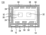
- 筐体と、
前記筐体内に設置され、電気回路が形成された回路基板と、
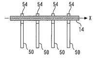
前記筐体内において互いに間隔をおいて並べられた複数の端子と、
を備え、
前記端子は、
前記筐体内で前記電気回路と電気的に接続される根元部と、
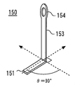
前記根元部の端において前記根元部から立ち上がるように前記根元部との間に折り目を付けて折り曲げられ、先端にプレスフィット部を有する胴体部と、
を有し、
前記折り目が前記根元部の長手方向軸に対して傾けられており、
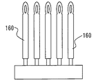
隣り合う前記端子同士で、それぞれの前記プレスフィット部がプレスフィットにより縮んだ状態から復元する方向が互いに逸らされた半導体装置。 - 複数のスルーホールを備え、前記複数のスルーホールそれぞれに前記複数の端子の前記プレスフィット部がはまり込むように前記回路基板に重ねられた他の基板と、
前記他の基板に形成された回路と電気的に接続し、前記筐体外に露出する主端子と、
を更に備える請求項1に記載の半導体装置。 - 前記複数の端子のプレスフィット部が、前記筐体の上面から前記筐体外へ突き出ている請求項1に記載の半導体装置。
- 前記電気回路は、半導体素子を含み、
前記半導体素子は、ワイドバンドギャップ半導体によって形成されている請求項1〜3のいずれか1項に記載の半導体装置。 - 少なくとも1つの半導体装置を備える電力変換装置であって、
前記半導体装置は、
筐体と、
前記筐体内に設置され、電気回路が形成された回路基板と、
前記筐体内において互いに間隔をおいて並べられた複数の端子と、
を備え、
前記端子は、
前記筐体内で前記電気回路と電気的に接続される根元部と、
前記根元部の端において前記根元部から立ち上がるように前記根元部との間に折り目を付けて折り曲げられ、先端にプレスフィット部を有する胴体部と、
を有し、
前記折り目が前記根元部の長手方向軸に対して傾けられており、
隣り合う前記端子同士で、それぞれの前記プレスフィット部がプレスフィットにより縮んだ状態から復元する方向が互いに逸らされた電力変換装置。 - 金属板を金型で打ち抜くことにより、根元部と前記根元部の端に接続した胴体部と前記胴体部の先端に設けられたプレスフィット部とを有し前記根元部の長手方向に対して前記胴体部の長手方向が傾けられた平板状のプレスフィット端子用板材を形成する工程と、
前記根元部の端において前記胴体部が前記根元部から立ち上がるように、かつ前記根元部の長手方向軸に対して折り目が傾くように、前記プレスフィット端子用板材の前記根元部と前記胴体部とを折り曲げることで、プレスフィット端子を形成する工程と、
を備えるプレスフィット端子の製造方法。 - 根元部と、
前記根元部の端において前記根元部から立ち上がるように前記根元部との間に折り目を付けて折り曲げられ、先端にプレスフィット部を有する胴体部と、
を有し、
前記折り目が前記根元部の長手方向軸に対して傾けられたプレスフィット端子。
Priority Applications (4)
| Application Number | Priority Date | Filing Date | Title |
|---|---|---|---|
| JP2015120421A JP6380244B2 (ja) | 2015-06-15 | 2015-06-15 | 半導体装置、電力変換装置 |
| US15/070,649 US9774112B2 (en) | 2015-06-15 | 2016-03-15 | Press-fit terminal, semiconductor device, power conversion apparatus and method of manufacturing press-fit terminal |
| DE102016209604.4A DE102016209604B4 (de) | 2015-06-15 | 2016-06-01 | Halbleitervorrichtung und Leistungswandlungsvorrichtung |
| CN201610424290.1A CN106252292B (zh) | 2015-06-15 | 2016-06-15 | 压接端子、半导体装置、电力变换装置及压接端子的制造方法 |
Applications Claiming Priority (1)
| Application Number | Priority Date | Filing Date | Title |
|---|---|---|---|
| JP2015120421A JP6380244B2 (ja) | 2015-06-15 | 2015-06-15 | 半導体装置、電力変換装置 |
Publications (2)
| Publication Number | Publication Date |
|---|---|
| JP2017005200A true JP2017005200A (ja) | 2017-01-05 |
| JP6380244B2 JP6380244B2 (ja) | 2018-08-29 |
Family
ID=57516290
Family Applications (1)
| Application Number | Title | Priority Date | Filing Date |
|---|---|---|---|
| JP2015120421A Active JP6380244B2 (ja) | 2015-06-15 | 2015-06-15 | 半導体装置、電力変換装置 |
Country Status (4)
| Country | Link |
|---|---|
| US (1) | US9774112B2 (ja) |
| JP (1) | JP6380244B2 (ja) |
| CN (1) | CN106252292B (ja) |
| DE (1) | DE102016209604B4 (ja) |
Families Citing this family (3)
| Publication number | Priority date | Publication date | Assignee | Title |
|---|---|---|---|---|
| US9979105B2 (en) * | 2015-05-15 | 2018-05-22 | Mitsubishi Electric Corporation | Power semiconductor device |
| JP7224272B2 (ja) * | 2019-10-30 | 2023-02-17 | 三菱電機株式会社 | パワー半導体装置 |
| KR102603439B1 (ko) * | 2022-03-07 | 2023-11-20 | 제엠제코(주) | 음각기판을 구비한 반도체 패키지 및 이의 제조방법 |
Citations (8)
| Publication number | Priority date | Publication date | Assignee | Title |
|---|---|---|---|---|
| US4393581A (en) * | 1980-01-22 | 1983-07-19 | Amp Incorporated | Method of forming leads on a lead frame |
| JPS63153548U (ja) * | 1987-03-27 | 1988-10-07 | ||
| US4906209A (en) * | 1987-10-01 | 1990-03-06 | Murata Manufacturing Co., Ltd. | Feed-through capacitor having a compliant pin terminal |
| JPH04131122U (ja) * | 1991-05-25 | 1992-12-02 | 古河電気工業株式会社 | 電気接続箱 |
| JPH0817501A (ja) * | 1994-06-30 | 1996-01-19 | Yamaichi Electron Co Ltd | 電気接触子 |
| JP2007329383A (ja) * | 2006-06-09 | 2007-12-20 | Toyota Industries Corp | 半導体モジュールの電極構造 |
| JP2010123415A (ja) * | 2008-11-20 | 2010-06-03 | Toyota Motor Corp | プレスフィット端子の挿入装置およびその方法と,プレスフィット端子と基板との結合品の製造方法 |
| WO2014132803A1 (ja) * | 2013-02-26 | 2014-09-04 | 三菱電機株式会社 | 電力用半導体装置 |
Family Cites Families (17)
| Publication number | Priority date | Publication date | Assignee | Title |
|---|---|---|---|---|
| US5144412A (en) * | 1987-02-19 | 1992-09-01 | Olin Corporation | Process for manufacturing plastic pin grid arrays and the product produced thereby |
| GB8706610D0 (en) * | 1987-03-19 | 1987-04-23 | Smith Ind Plc | Electrical components |
| JP3367078B2 (ja) * | 1996-10-22 | 2003-01-14 | ローム株式会社 | ホトインタラプタ |
| JP2001023715A (ja) * | 1999-07-12 | 2001-01-26 | Sumitomo Wiring Syst Ltd | 端子金具 |
| JP2004063688A (ja) * | 2002-07-26 | 2004-02-26 | Mitsubishi Electric Corp | 半導体装置及び半導体アセンブリモジュール |
| US7491897B2 (en) * | 2002-09-30 | 2009-02-17 | Fujitsu Ten Limited | Electronic equipment provided with wiring board into which press-fit terminals are press-fitted |
| EP1795496A2 (en) * | 2005-12-08 | 2007-06-13 | Yamaha Corporation | Semiconductor device for detecting pressure variations |
| JP4410242B2 (ja) * | 2006-12-27 | 2010-02-03 | 三菱電機株式会社 | 電子制御装置及びその製造方法 |
| JP4634498B2 (ja) * | 2008-11-28 | 2011-02-16 | 三菱電機株式会社 | 電力用半導体モジュール |
| DE102009025113A1 (de) * | 2009-06-11 | 2010-12-16 | Continental Teves Ag & Co. Ohg | Einpresskontakt zur Verbindung eines elektronischen Bauelementes mit einer Leiterplatte sowie Einpresswerkzeug |
| DE102010038727B4 (de) * | 2010-07-30 | 2015-07-16 | Infineon Technologies Ag | Leistungshaltleitermodul und Verfahren zur Herstellung eines Leistungshalbleitermoduls |
| US8581377B2 (en) * | 2010-09-16 | 2013-11-12 | Tessera, Inc. | TSOP with impedance control |
| JP5383621B2 (ja) * | 2010-10-20 | 2014-01-08 | 三菱電機株式会社 | パワー半導体装置 |
| JP5599328B2 (ja) | 2011-01-20 | 2014-10-01 | 三菱電機株式会社 | 電力用半導体装置とプリント配線板との接続機構 |
| JP5531974B2 (ja) * | 2011-01-21 | 2014-06-25 | 住友電装株式会社 | コネクタ及び端子整列部材 |
| US8742555B2 (en) * | 2011-08-30 | 2014-06-03 | Jian Wen | Lead frame having a flag with in-plane and out-of-plane mold locking features |
| WO2014110563A1 (en) | 2013-01-14 | 2014-07-17 | Vishay General Semiconductor Llc | Electrical press-fit pin for a semiconductor module |
-
2015
- 2015-06-15 JP JP2015120421A patent/JP6380244B2/ja active Active
-
2016
- 2016-03-15 US US15/070,649 patent/US9774112B2/en active Active
- 2016-06-01 DE DE102016209604.4A patent/DE102016209604B4/de active Active
- 2016-06-15 CN CN201610424290.1A patent/CN106252292B/zh active Active
Patent Citations (8)
| Publication number | Priority date | Publication date | Assignee | Title |
|---|---|---|---|---|
| US4393581A (en) * | 1980-01-22 | 1983-07-19 | Amp Incorporated | Method of forming leads on a lead frame |
| JPS63153548U (ja) * | 1987-03-27 | 1988-10-07 | ||
| US4906209A (en) * | 1987-10-01 | 1990-03-06 | Murata Manufacturing Co., Ltd. | Feed-through capacitor having a compliant pin terminal |
| JPH04131122U (ja) * | 1991-05-25 | 1992-12-02 | 古河電気工業株式会社 | 電気接続箱 |
| JPH0817501A (ja) * | 1994-06-30 | 1996-01-19 | Yamaichi Electron Co Ltd | 電気接触子 |
| JP2007329383A (ja) * | 2006-06-09 | 2007-12-20 | Toyota Industries Corp | 半導体モジュールの電極構造 |
| JP2010123415A (ja) * | 2008-11-20 | 2010-06-03 | Toyota Motor Corp | プレスフィット端子の挿入装置およびその方法と,プレスフィット端子と基板との結合品の製造方法 |
| WO2014132803A1 (ja) * | 2013-02-26 | 2014-09-04 | 三菱電機株式会社 | 電力用半導体装置 |
Also Published As
| Publication number | Publication date |
|---|---|
| US9774112B2 (en) | 2017-09-26 |
| CN106252292B (zh) | 2019-06-25 |
| JP6380244B2 (ja) | 2018-08-29 |
| CN106252292A (zh) | 2016-12-21 |
| US20160365662A1 (en) | 2016-12-15 |
| DE102016209604A1 (de) | 2017-01-12 |
| DE102016209604B4 (de) | 2023-03-30 |
Similar Documents
| Publication | Publication Date | Title |
|---|---|---|
| JP6316504B2 (ja) | 電力用半導体装置 | |
| CN107278322B (zh) | 电器件和用于制造电器件的方法 | |
| JP2004221052A (ja) | コンタクトシート及びその製造方法並びにソケット | |
| US9443818B2 (en) | Power semiconductor module | |
| US6532654B2 (en) | Method of forming an electrical connector | |
| JP2017139304A (ja) | 電極端子、半導体装置及び電力変換装置 | |
| CN108028479A (zh) | 半导体装置、金属电极部件及半导体装置的制造方法 | |
| JP6380244B2 (ja) | 半導体装置、電力変換装置 | |
| JP6406983B2 (ja) | 半導体装置およびその製造方法 | |
| JP4570092B2 (ja) | 半導体モジュール | |
| JP2005045237A (ja) | 等級分け可能な構造技術によるパワー半導体モジュール | |
| CN107622979B (zh) | 半导体装置以及半导体装置用壳体 | |
| JP2015026791A (ja) | 半導体装置及びリードフレーム | |
| JPH0636852A (ja) | プリント配線板への端子の接続法 | |
| JP2002009217A (ja) | 樹脂封止型半導体装置 | |
| JP2008294219A (ja) | 半導体装置及びその製造方法 | |
| KR101629470B1 (ko) | 전력용 반도체 모듈의 조립방법 및 이를 이용하여 제조된 전력용 반도체 모듈 | |
| KR101698431B1 (ko) | 반도체 파워 모듈 패키지 및 그의 제조방법 | |
| JP3163214U (ja) | 半導体装置 | |
| CN105848415B (zh) | 侧边具有表面黏着型接脚的电路模块以及电路板与系统 | |
| JP6381439B2 (ja) | ケーブル接続構造 | |
| JP2013069746A (ja) | 半導体装置および電極端子 | |
| JP2016018821A (ja) | 半導体装置の製造方法、半導体装置、及び、リードフレーム | |
| JP2006060106A (ja) | リード部材及び表面実装型半導体装置 | |
| JP4622646B2 (ja) | 半導体装置 |
Legal Events
| Date | Code | Title | Description |
|---|---|---|---|
| A621 | Written request for application examination |
Free format text: JAPANESE INTERMEDIATE CODE: A621 Effective date: 20170516 |
|
| A977 | Report on retrieval |
Free format text: JAPANESE INTERMEDIATE CODE: A971007 Effective date: 20180206 |
|
| A131 | Notification of reasons for refusal |
Free format text: JAPANESE INTERMEDIATE CODE: A131 Effective date: 20180213 |
|
| A521 | Request for written amendment filed |
Free format text: JAPANESE INTERMEDIATE CODE: A523 Effective date: 20180323 |
|
| TRDD | Decision of grant or rejection written | ||
| A01 | Written decision to grant a patent or to grant a registration (utility model) |
Free format text: JAPANESE INTERMEDIATE CODE: A01 Effective date: 20180703 |
|
| A61 | First payment of annual fees (during grant procedure) |
Free format text: JAPANESE INTERMEDIATE CODE: A61 Effective date: 20180716 |
|
| R150 | Certificate of patent or registration of utility model |
Ref document number: 6380244 Country of ref document: JP Free format text: JAPANESE INTERMEDIATE CODE: R150 |
|
| R250 | Receipt of annual fees |
Free format text: JAPANESE INTERMEDIATE CODE: R250 |
|
| R250 | Receipt of annual fees |
Free format text: JAPANESE INTERMEDIATE CODE: R250 |
|
| R250 | Receipt of annual fees |
Free format text: JAPANESE INTERMEDIATE CODE: R250 |
|
| R250 | Receipt of annual fees |
Free format text: JAPANESE INTERMEDIATE CODE: R250 |
|
| R250 | Receipt of annual fees |
Free format text: JAPANESE INTERMEDIATE CODE: R250 |