WO2014136473A1 - Dispositif d'oscillation à quartz - Google Patents
Dispositif d'oscillation à quartz Download PDFInfo
- Publication number
- WO2014136473A1 WO2014136473A1 PCT/JP2014/050428 JP2014050428W WO2014136473A1 WO 2014136473 A1 WO2014136473 A1 WO 2014136473A1 JP 2014050428 W JP2014050428 W JP 2014050428W WO 2014136473 A1 WO2014136473 A1 WO 2014136473A1
- Authority
- WO
- WIPO (PCT)
- Prior art keywords
- crystal
- substrate
- quartz
- conductive adhesive
- resonator
- Prior art date
- Legal status (The legal status is an assumption and is not a legal conclusion. Google has not performed a legal analysis and makes no representation as to the accuracy of the status listed.)
- Ceased
Links
Images



Classifications
-
- H—ELECTRICITY
- H03—ELECTRONIC CIRCUITRY
- H03H—IMPEDANCE NETWORKS, e.g. RESONANT CIRCUITS; RESONATORS
- H03H9/00—Networks comprising electromechanical or electro-acoustic elements; Electromechanical resonators
- H03H9/02—Details
- H03H9/05—Holders or supports
- H03H9/10—Mounting in enclosures
- H03H9/1007—Mounting in enclosures for bulk acoustic wave [BAW] devices
- H03H9/1014—Mounting in enclosures for bulk acoustic wave [BAW] devices the enclosure being defined by a frame built on a substrate and a cap, the frame having no mechanical contact with the BAW device
- H03H9/1021—Mounting in enclosures for bulk acoustic wave [BAW] devices the enclosure being defined by a frame built on a substrate and a cap, the frame having no mechanical contact with the BAW device the BAW device being of the cantilever type
-
- H—ELECTRICITY
- H03—ELECTRONIC CIRCUITRY
- H03H—IMPEDANCE NETWORKS, e.g. RESONANT CIRCUITS; RESONATORS
- H03H9/00—Networks comprising electromechanical or electro-acoustic elements; Electromechanical resonators
- H03H9/02—Details
- H03H9/05—Holders or supports
- H03H9/09—Elastic or damping supports
-
- H—ELECTRICITY
- H03—ELECTRONIC CIRCUITRY
- H03H—IMPEDANCE NETWORKS, e.g. RESONANT CIRCUITS; RESONATORS
- H03H9/00—Networks comprising electromechanical or electro-acoustic elements; Electromechanical resonators
- H03H9/15—Constructional features of resonators consisting of piezoelectric or electrostrictive material
- H03H9/17—Constructional features of resonators consisting of piezoelectric or electrostrictive material having a single resonator
- H03H9/19—Constructional features of resonators consisting of piezoelectric or electrostrictive material having a single resonator consisting of quartz
-
- H—ELECTRICITY
- H10—SEMICONDUCTOR DEVICES; ELECTRIC SOLID-STATE DEVICES NOT OTHERWISE PROVIDED FOR
- H10N—ELECTRIC SOLID-STATE DEVICES NOT OTHERWISE PROVIDED FOR
- H10N30/00—Piezoelectric or electrostrictive devices
- H10N30/80—Constructional details
- H10N30/87—Electrodes or interconnections, e.g. leads or terminals
-
- H—ELECTRICITY
- H03—ELECTRONIC CIRCUITRY
- H03H—IMPEDANCE NETWORKS, e.g. RESONANT CIRCUITS; RESONATORS
- H03H9/00—Networks comprising electromechanical or electro-acoustic elements; Electromechanical resonators
- H03H9/02—Details
- H03H9/125—Driving means, e.g. electrodes, coils
- H03H9/13—Driving means, e.g. electrodes, coils for networks consisting of piezoelectric or electrostrictive materials
- H03H9/132—Driving means, e.g. electrodes, coils for networks consisting of piezoelectric or electrostrictive materials characterized by a particular shape
Definitions
- the present invention relates to a crystal vibration device using a crystal resonator, and more particularly to a crystal vibration device in which a crystal resonator is mounted on a case substrate with a conductive adhesive.
- Patent Literature 1 discloses a piezoelectric device in which a crystal resonator is supported by a cantilever with respect to a base substrate. This crystal resonator is configured by using an AT-cut crystal resonator element whose main vibration is thickness shear vibration. The crystal resonator is fixed to the base substrate by a support mount.
- the support mount is made of epoxy resin or silicone resin.
- Patent Document 2 discloses a piezoelectric device using a crystal resonator.
- a quartz resonator is sealed in a substrate, a seal ring, a lid made of metal, and a package.
- This crystal unit is supported by a cantilever on the substrate.
- the crystal resonator is bonded to the substrate using a conductive adhesive.
- Patent Document 2 describes that the size of the conductive adhesive in the width direction of the crystal resonator is within a specific range.
- the support mount is constituted by an epoxy resin or a silicone resin.
- ESR equivalent series resistance
- Patent Document 2 although the dimensions of the conductive adhesive in the width direction of the crystal unit are described, the dimensions in the long side direction of the crystal unit are not described. Also in the piezoelectric device described in Patent Document 2, vibration may be damped depending on the application mode of the conductive adhesive bonding the crystal resonator. That is, good vibration characteristics could not be obtained with certainty.
- An object of the present invention is to provide a crystal vibration device in which deterioration of ESR characteristics due to a conductive adhesive hardly occurs.
- the crystal vibration device includes a case substrate, first and second attachment electrodes, a crystal resonator, and first and second conductive adhesive layers.
- the first and second attachment electrodes are formed on the upper surface of the case substrate.
- the crystal resonator is mounted on a case substrate and is formed using an AT cut crystal substrate.
- the first and second conductive adhesive layers electrically connect the crystal unit to the first and second attachment electrodes and support the crystal unit with a cantilever beam.
- the total bonding area S (mm 2 ) of the bonding portion where the crystal resonator is bonded to the case substrate by the first and second conductive adhesive layers is when the thickness of the crystal substrate is t ( ⁇ m). , S ⁇ ⁇ 0.001t + 0.22.
- the crystal substrate constituting the crystal resonator is supported by a cantilever at one end in the length direction, and the length direction of the crystal resonator is The direction is the X-axis direction.
- the X-axis direction is the length direction, it is supported by a cantilever on the short side. In that case, although the influence of vibration restraint by the support structure is large, the degradation of the ESR characteristic can be effectively suppressed according to the present invention.
- the conductive adhesive layer is made of an epoxy resin adhesive having an epoxy resin and a conductive material dispersed in the epoxy resin.
- the crystal unit can be firmly mechanically supported by the case substrate.
- the crystal resonator includes a first excitation electrode provided on an upper surface of a crystal substrate, a lower surface, and the first excitation electrode. It has the 2nd excitation electrode which overlaps, and the 1st, 2nd terminal electrode provided in the lower surface of the said quartz substrate electrically connected to the said 1st and 2nd excitation electrode.
- the junction area S is in the specific range, it is possible to effectively suppress the deterioration of the ESR characteristics. Therefore, it is possible to provide a crystal vibration device with good characteristics.
- FIG. 1 is an exploded perspective view of a quartz crystal vibration device according to an embodiment of the present invention.
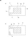
- FIGS. 2A and 2B are a plan view and a schematic plan view showing the electrode structure on the lower surface of the crystal resonator used in the crystal vibration device of one embodiment of the present invention.
- FIG. 3 is a schematic plan view for explaining the bonding area S in one embodiment of the present invention.
- FIG. 4 is a diagram showing the relationship between the junction area S and the equivalent series resistance ESR in a crystal resonator having an oscillation frequency of 24 MHz.
- FIG. 5 is a diagram showing the relationship between the junction area S and the equivalent series resistance ESR in the crystal vibration device having the oscillation frequency of 30 MHz.
- FIG. 6 is a diagram illustrating the relationship between the thickness t of the quartz substrate and the bonding area S in which ESR damping is suppressed.
- FIG. 1 is an exploded perspective view of a quartz crystal vibration device according to an embodiment of the present invention.
- the crystal vibration device 1 has a case substrate 2.
- the case substrate 2 is made of an appropriate insulating material. Examples of such an insulating material include insulating ceramics such as alumina and synthetic resins.
- First and second mounting electrodes 3 and 4 are formed on the upper surface of the case substrate 2.
- the first attachment electrode 3 is drawn out to one corner portion of the case substrate 2 by the wiring electrode 5.
- a first external electrode 6 is formed at the corner portion.
- the first external electrode 6 is provided on the inner peripheral surface of a recess provided by cutting out a corner portion.
- the second attachment electrode 4 is electrically connected to the second external electrode 8 by the wiring electrode 7.
- the second external electrode 8 is provided at a corner portion that is diagonal to the corner portion where the first external electrode 6 is formed.
- Dummy electrodes 9 and 10 connected to the ground potential are formed at the remaining two corners.
- the first and second mounting electrodes 3 and 4, the wiring electrodes 5 and 7, the first and second external electrodes 6 and 8, and the dummy electrodes 9 and 10 are made of an appropriate metal or alloy such as Al or Cu. Is formed.
- a crystal resonator 11 is joined by first and second conductive adhesive layers 12 and 13.
- the crystal unit 11 has an AT-cut crystal substrate 14.
- the AT-cut quartz crystal substrate 14 has a rectangular plate shape having a length direction.
- the length direction is the X-axis direction of the crystal.
- a first excitation electrode 15 is formed on the upper surface of the quartz substrate 14.
- a second excitation electrode 16 is formed on the lower surface of the quartz substrate 14.
- the first excitation electrode 15 and the second excitation electrode 16 are disposed so as to overlap with each other with the crystal substrate 14 interposed therebetween.
- the first and second excitation electrodes 15 and 16 are formed at the center of the upper surface and the lower surface of the quartz substrate 14. Therefore, the energy confinement type vibration part is configured using the first and second excitation electrodes 15 and 16.
- the planar shape of the quartz substrate 14 has a pair of opposing long sides 14a and 14b and a pair of opposing short sides 14c and 14d.
- the first excitation electrode 15 is connected to the extraction electrode 17.
- the extraction electrode 17 is extracted to a corner portion formed by the short side 14c and the long side 14b.
- the lead electrode 17 is electrically connected to the first terminal electrode 18 shown in FIG. That is, the lead electrode 17 obtains the side surface on the short side 14 c side at the corner portion of the quartz substrate 14, reaches the lower surface, and is electrically connected to the first terminal electrode 18 provided on the lower surface.
- the second excitation electrode 16 is connected to the extraction electrode 19 provided on the lower surface of the quartz substrate 14.
- the lead electrode 19 is electrically connected to a second terminal electrode 20 provided at a corner formed by the short side 14c and the long side 14a.
- the first and second terminal electrodes 18 and 20 are located on both sides of the short side 14 c on the lower surface of the quartz substrate 14.
- the first and second excitation electrodes 15 and 16, the extraction electrodes 17 and 19 and the first and second terminal electrodes 18 and 20 are also formed of an appropriate metal or alloy such as Al or Cu.
- the crystal resonator 11 includes the first and second terminal electrodes 18 and 20 shown in FIG. 2 through the first and second conductive adhesive layers 12 and 13.
- the second attachment electrodes 3 and 4 are electrically connected and mechanically joined. Accordingly, the crystal unit 11 is supported by a cantilever at one end in the length direction.
- the conductive adhesive layers 12 and 13 are formed of an epoxy resin adhesive having an epoxy resin and a conductive material such as a metal powder dispersed in the epoxy resin.
- the epoxy resin adhesive the hardness of the cured product is high. Therefore, the crystal unit 11 can be more firmly supported by the cantilever.
- the material constituting the conductive adhesive layer is not limited to the epoxy resin adhesive, but may be one using other synthetic resin such as silicone resin other than epoxy resin, polyid resin. .
- a thermosetting resin is preferable, but a resin other than the thermosetting resin may be used.
- an appropriate conductive material such as carbon powder can be used in addition to the metal powder.
- the feature of the quartz crystal vibrating device 1 is that the bonding area S by the first and second conductive adhesive layers 12 and 13 is S (mm 2 ) ⁇ ⁇ when the thickness of the quartz crystal substrate 14 is t ( ⁇ m). It is in the range of 0.001t + 0.22. Thereby, ESR damping can be effectively suppressed. This will be described with reference to FIGS.
- FIG. 3 is a schematic plan view for explaining the bonding area S.
- the crystal unit 11 is indicated by a broken line.
- the first and second conductive adhesive layers 12 and 13 are bonded to the lower surface of the crystal unit 11.
- FIG. 4 is a diagram showing a change in ESR when the crystal vibration device 1 having an oscillation frequency of 24 MHz is manufactured and the junction area S is variously changed.
- the ESR damping increases as the junction area S increases. It can also be seen that the ESR values vary considerably even when the junction areas S are equal. On the other hand, when S is less than 0.150 mm 2 , it can be seen that the value of ESR does not vary and the ESR is low and stable. That is, it can be seen that, in the crystal vibration device 1 having an oscillation frequency of 24 MHz, ESR damping can be suppressed by setting the junction area S to less than 0.150 mm 2 .
- FIG. 5 is a diagram showing changes in ESR when the junction area S is variously changed in the same manner for the crystal vibration device 1 having an oscillation frequency of 30 MHz. As can be seen from FIG. 5, when the oscillation frequency is 30 MHz, the junction area S should be less than 0.16 mm 2 .
- the inventors of the present application further changed the oscillation frequency and examined the relationship between the junction area S and ESR damping.
- the results are shown in FIG.
- junction area S was smaller than this straight line A, it discovered that ESR damping could be suppressed effectively like the stable area
- the frequency constant of a quartz substrate made of AT cut quartz is 1670 MHz ⁇ ⁇ m.
- the relationship of the above-described formula S ⁇ ⁇ 0.001t + 0.22 is based on the frequency constant of the AT cut crystal.
- junction area S is smaller than ⁇ 0.001t + 0.22, ESR damping can be effectively suppressed.
- the quartz substrate 14 is made of an AT-cut quartz substrate as described above, and its length direction is the X-axis direction of the quartz.
- the crystal unit 11 is supported by a cantilever on one end in the length direction, that is, supported on the short side. Therefore, the influence of restraint by mechanical support is great.
- the bonding area S is in a specific range, the influence of vibration restraint can be effectively suppressed. That is, ESR damping can be effectively suppressed.
- a cap 21 opened downward is fixed to the upper surface of the case substrate 2 so as to surround the crystal resonator 11.
- This fixing can be performed using an appropriate adhesive such as an epoxy resin adhesive.
- the cap 21 is made of metal and has a shape opened downward. Therefore, in the crystal device 1, since the package is configured using the cap 21, the size can be reduced.
- the crystal unit 11 may be sealed using another package material instead of the cap 21.
Landscapes
- Physics & Mathematics (AREA)
- Acoustics & Sound (AREA)
- Piezo-Electric Or Mechanical Vibrators, Or Delay Or Filter Circuits (AREA)
Abstract
L'invention concerne un dispositif d'oscillation à quartz par lequel un amortissement ESR est rendu minimal de manière efficace. Dans ce dispositif d'oscillation à quartz (1), un oscillateur à quartz (11) est porté de manière en porte-à-faux par des première et seconde couches conductrices (12, 13) sur un substrat de boîtier (2), l'oscillateur à quartz (11) étant électriquement connecté à des première et seconde électrodes fixes (3, 4). S ≤ -0,001t + 0,22, S (mm²) représentant la somme de la surface jointe des sections jointes dans lesquelles l'oscillateur à quartz (11) est joint au substrat de boîtier (2) par les première et seconde couches conductrices (12, 13), et t (µm) représentant l'épaisseur du substrat de quartz (14).
Priority Applications (2)
| Application Number | Priority Date | Filing Date | Title |
|---|---|---|---|
| JP2015504193A JP6075441B2 (ja) | 2013-03-07 | 2014-01-14 | 水晶振動装置 |
| US14/833,559 US9509275B2 (en) | 2013-03-07 | 2015-08-24 | Quartz vibrating device with conductive adhesive layers having specific bonding surface area |
Applications Claiming Priority (2)
| Application Number | Priority Date | Filing Date | Title |
|---|---|---|---|
| JP2013-045680 | 2013-03-07 | ||
| JP2013045680 | 2013-03-07 |
Related Child Applications (1)
| Application Number | Title | Priority Date | Filing Date |
|---|---|---|---|
| US14/833,559 Continuation US9509275B2 (en) | 2013-03-07 | 2015-08-24 | Quartz vibrating device with conductive adhesive layers having specific bonding surface area |
Publications (1)
| Publication Number | Publication Date |
|---|---|
| WO2014136473A1 true WO2014136473A1 (fr) | 2014-09-12 |
Family
ID=51491005
Family Applications (1)
| Application Number | Title | Priority Date | Filing Date |
|---|---|---|---|
| PCT/JP2014/050428 Ceased WO2014136473A1 (fr) | 2013-03-07 | 2014-01-14 | Dispositif d'oscillation à quartz |
Country Status (3)
| Country | Link |
|---|---|
| US (1) | US9509275B2 (fr) |
| JP (1) | JP6075441B2 (fr) |
| WO (1) | WO2014136473A1 (fr) |
Families Citing this family (2)
| Publication number | Priority date | Publication date | Assignee | Title |
|---|---|---|---|---|
| USD760230S1 (en) | 2014-09-16 | 2016-06-28 | Daishinku Corporation | Piezoelectric vibration device |
| KR101715183B1 (ko) * | 2015-06-01 | 2017-03-10 | 주식회사 성광이엔지 | 가축용 사료탱크의 사료배출장치 |
Citations (6)
| Publication number | Priority date | Publication date | Assignee | Title |
|---|---|---|---|---|
| JPH03175713A (ja) * | 1989-12-04 | 1991-07-30 | Murata Mfg Co Ltd | 圧電共振子とその製造方法 |
| JP2002100950A (ja) * | 2000-09-22 | 2002-04-05 | Kyocera Corp | 圧電デバイス |
| JP2006211089A (ja) * | 2005-01-26 | 2006-08-10 | Daishinku Corp | 圧電振動デバイス |
| JP2009188484A (ja) * | 2008-02-04 | 2009-08-20 | Epson Toyocom Corp | 圧電フィルタ |
| JP2010178184A (ja) * | 2009-01-30 | 2010-08-12 | Nippon Dempa Kogyo Co Ltd | 水晶振動子の製造方法 |
| JP2013027003A (ja) * | 2011-07-26 | 2013-02-04 | Nippon Dempa Kogyo Co Ltd | 圧電デバイス |
Family Cites Families (9)
| Publication number | Priority date | Publication date | Assignee | Title |
|---|---|---|---|---|
| JP2000138550A (ja) * | 1998-10-29 | 2000-05-16 | Toyo Commun Equip Co Ltd | 表面実装型圧電デバイス |
| JP2001077651A (ja) | 1999-08-31 | 2001-03-23 | Kyocera Corp | 圧電デバイス |
| JP4087186B2 (ja) * | 2002-06-25 | 2008-05-21 | 日本電波工業株式会社 | 水晶振動子の保持構造 |
| JP4222147B2 (ja) * | 2002-10-23 | 2009-02-12 | セイコーエプソン株式会社 | 圧電発振器及び圧電発振器を利用した携帯電話装置および圧電発振器を利用した電子機器 |
| JP2005197957A (ja) | 2004-01-06 | 2005-07-21 | Toyo Commun Equip Co Ltd | 圧電振動子、及び圧電発振器 |
| JP2011182155A (ja) | 2010-03-01 | 2011-09-15 | Seiko Epson Corp | 圧電デバイスと圧電デバイスの製造方法 |
| JP2013021667A (ja) * | 2011-03-23 | 2013-01-31 | Nippon Dempa Kogyo Co Ltd | 水晶デバイス |
| JP2012199861A (ja) * | 2011-03-23 | 2012-10-18 | Nippon Dempa Kogyo Co Ltd | 水晶デバイス及び水晶デバイスの検査方法 |
| JP5839146B2 (ja) * | 2013-04-08 | 2016-01-06 | 株式会社村田製作所 | 水晶振動装置 |
-
2014
- 2014-01-14 WO PCT/JP2014/050428 patent/WO2014136473A1/fr not_active Ceased
- 2014-01-14 JP JP2015504193A patent/JP6075441B2/ja active Active
-
2015
- 2015-08-24 US US14/833,559 patent/US9509275B2/en active Active
Patent Citations (6)
| Publication number | Priority date | Publication date | Assignee | Title |
|---|---|---|---|---|
| JPH03175713A (ja) * | 1989-12-04 | 1991-07-30 | Murata Mfg Co Ltd | 圧電共振子とその製造方法 |
| JP2002100950A (ja) * | 2000-09-22 | 2002-04-05 | Kyocera Corp | 圧電デバイス |
| JP2006211089A (ja) * | 2005-01-26 | 2006-08-10 | Daishinku Corp | 圧電振動デバイス |
| JP2009188484A (ja) * | 2008-02-04 | 2009-08-20 | Epson Toyocom Corp | 圧電フィルタ |
| JP2010178184A (ja) * | 2009-01-30 | 2010-08-12 | Nippon Dempa Kogyo Co Ltd | 水晶振動子の製造方法 |
| JP2013027003A (ja) * | 2011-07-26 | 2013-02-04 | Nippon Dempa Kogyo Co Ltd | 圧電デバイス |
Also Published As
| Publication number | Publication date |
|---|---|
| JPWO2014136473A1 (ja) | 2017-02-09 |
| US9509275B2 (en) | 2016-11-29 |
| JP6075441B2 (ja) | 2017-02-08 |
| US20150365068A1 (en) | 2015-12-17 |
Similar Documents
| Publication | Publication Date | Title |
|---|---|---|
| US11075615B2 (en) | Crystal vibration element, and crystal vibrator equipped with crystal vibration element | |
| KR101219211B1 (ko) | 진동편, 진동자, 발진기, 전자기기, 및 주파수 조정 방법 | |
| JP5756712B2 (ja) | 水晶デバイス | |
| JP5804825B2 (ja) | 水晶振動素子及び水晶デバイス | |
| JP5699809B2 (ja) | 圧電振動片 | |
| JP2015186196A (ja) | 圧電振動片及び圧電デバイス | |
| JP2013066109A (ja) | 圧電デバイス | |
| JP2017152943A (ja) | 水晶振動素子及び水晶振動デバイス | |
| JP6075441B2 (ja) | 水晶振動装置 | |
| WO2014178308A1 (fr) | Dispositif d'oscillation de cristal et procédé de fabrication associé | |
| US10985727B2 (en) | Piezoelectric vibrator | |
| JP5839146B2 (ja) | 水晶振動装置 | |
| JP6611524B2 (ja) | 圧電振動片および圧電振動子 | |
| WO2014162896A1 (fr) | Dispositif oscillateur à cristal | |
| JP5637868B2 (ja) | 圧電デバイス及び圧電デバイスの製造方法 | |
| JP6577791B2 (ja) | 水晶素板、水晶振動素子及び水晶デバイス | |
| JP6181904B1 (ja) | 圧電部品 | |
| JP6086950B2 (ja) | 水晶振動素子及び水晶デバイス | |
| JP2008005089A (ja) | 輪郭振動片、輪郭振動子 | |
| JP2005198193A (ja) | 圧電振動部品 | |
| JP2020072298A (ja) | 振動素子用の台座、振動子及び発振器 | |
| JP2011199333A (ja) | 圧電振動片および圧電デバイス | |
| JP2008278011A (ja) | 圧電振動部品 | |
| JP2008004991A (ja) | 輪郭振動片、輪郭振動子 | |
| JP2012186638A (ja) | 圧電振動片、圧電振動子、電子デバイス |
Legal Events
| Date | Code | Title | Description |
|---|---|---|---|
| 121 | Ep: the epo has been informed by wipo that ep was designated in this application |
Ref document number: 14759918 Country of ref document: EP Kind code of ref document: A1 |
|
| ENP | Entry into the national phase |
Ref document number: 2015504193 Country of ref document: JP Kind code of ref document: A |
|
| NENP | Non-entry into the national phase |
Ref country code: DE |
|
| 122 | Ep: pct application non-entry in european phase |
Ref document number: 14759918 Country of ref document: EP Kind code of ref document: A1 |