WO2014136726A1 - Appareil de transmission, appareil de réception, et système de communication - Google Patents
Appareil de transmission, appareil de réception, et système de communication Download PDFInfo
- Publication number
- WO2014136726A1 WO2014136726A1 PCT/JP2014/055311 JP2014055311W WO2014136726A1 WO 2014136726 A1 WO2014136726 A1 WO 2014136726A1 JP 2014055311 W JP2014055311 W JP 2014055311W WO 2014136726 A1 WO2014136726 A1 WO 2014136726A1
- Authority
- WO
- WIPO (PCT)
- Prior art keywords
- symbol
- signal
- unit
- data
- block
- Prior art date
- Legal status (The legal status is an assumption and is not a legal conclusion. Google has not performed a legal analysis and makes no representation as to the accuracy of the status listed.)
- Ceased
Links
Images






Classifications
-
- H—ELECTRICITY
- H04—ELECTRIC COMMUNICATION TECHNIQUE
- H04L—TRANSMISSION OF DIGITAL INFORMATION, e.g. TELEGRAPHIC COMMUNICATION
- H04L27/00—Modulated-carrier systems
- H04L27/26—Systems using multi-frequency codes
- H04L27/2601—Multicarrier modulation systems
- H04L27/2626—Arrangements specific to the transmitter only
- H04L27/2627—Modulators
- H04L27/2634—Inverse fast Fourier transform [IFFT] or inverse discrete Fourier transform [IDFT] modulators in combination with other circuits for modulation
- H04L27/2636—Inverse fast Fourier transform [IFFT] or inverse discrete Fourier transform [IDFT] modulators in combination with other circuits for modulation with FFT or DFT modulators, e.g. standard single-carrier frequency-division multiple access [SC-FDMA] transmitter or DFT spread orthogonal frequency division multiplexing [DFT-SOFDM]
-
- H—ELECTRICITY
- H04—ELECTRIC COMMUNICATION TECHNIQUE
- H04L—TRANSMISSION OF DIGITAL INFORMATION, e.g. TELEGRAPHIC COMMUNICATION
- H04L27/00—Modulated-carrier systems
- H04L27/26—Systems using multi-frequency codes
- H04L27/2601—Multicarrier modulation systems
- H04L27/2602—Signal structure
-
- H—ELECTRICITY
- H04—ELECTRIC COMMUNICATION TECHNIQUE
- H04L—TRANSMISSION OF DIGITAL INFORMATION, e.g. TELEGRAPHIC COMMUNICATION
- H04L27/00—Modulated-carrier systems
- H04L27/26—Systems using multi-frequency codes
- H04L27/2601—Multicarrier modulation systems
- H04L27/2626—Arrangements specific to the transmitter only
- H04L27/26265—Arrangements for sidelobes suppression specially adapted to multicarrier systems, e.g. spectral precoding
-
- H—ELECTRICITY
- H04—ELECTRIC COMMUNICATION TECHNIQUE
- H04L—TRANSMISSION OF DIGITAL INFORMATION, e.g. TELEGRAPHIC COMMUNICATION
- H04L27/00—Modulated-carrier systems
- H04L27/26—Systems using multi-frequency codes
- H04L27/2601—Multicarrier modulation systems
- H04L27/2626—Arrangements specific to the transmitter only
- H04L27/2627—Modulators
- H04L27/2644—Modulators with oversampling
-
- H—ELECTRICITY
- H04—ELECTRIC COMMUNICATION TECHNIQUE
- H04L—TRANSMISSION OF DIGITAL INFORMATION, e.g. TELEGRAPHIC COMMUNICATION
- H04L27/00—Modulated-carrier systems
- H04L27/26—Systems using multi-frequency codes
- H04L27/2601—Multicarrier modulation systems
- H04L27/2647—Arrangements specific to the receiver only
- H04L27/2655—Synchronisation arrangements
- H04L27/2668—Details of algorithms
- H04L27/2673—Details of algorithms characterised by synchronisation parameters
- H04L27/2676—Blind, i.e. without using known symbols
- H04L27/2678—Blind, i.e. without using known symbols using cyclostationarities, e.g. cyclic prefix or postfix
-
- H—ELECTRICITY
- H04—ELECTRIC COMMUNICATION TECHNIQUE
- H04L—TRANSMISSION OF DIGITAL INFORMATION, e.g. TELEGRAPHIC COMMUNICATION
- H04L1/00—Arrangements for detecting or preventing errors in the information received
- H04L1/004—Arrangements for detecting or preventing errors in the information received by using forward error control
- H04L1/0041—Arrangements at the transmitter end
-
- H—ELECTRICITY
- H04—ELECTRIC COMMUNICATION TECHNIQUE
- H04L—TRANSMISSION OF DIGITAL INFORMATION, e.g. TELEGRAPHIC COMMUNICATION
- H04L25/00—Baseband systems
- H04L25/02—Details ; arrangements for supplying electrical power along data transmission lines
- H04L25/0202—Channel estimation
- H04L25/0224—Channel estimation using sounding signals
- H04L25/0228—Channel estimation using sounding signals with direct estimation from sounding signals
- H04L25/023—Channel estimation using sounding signals with direct estimation from sounding signals with extension to other symbols
- H04L25/0232—Channel estimation using sounding signals with direct estimation from sounding signals with extension to other symbols by interpolation between sounding signals
Definitions
- the present invention relates to a transmission device, a reception device, and a communication system.
- transmission path frequency selectivity and time variation occur due to multipath fading caused by reflection of a transmission signal on a building or the like and Doppler fluctuation caused by movement of a terminal.
- the received signal is a signal that interferes with a transmitted symbol and a symbol that arrives after a delay time.
- a single carrier block transmission method has recently attracted attention in order to obtain the best reception characteristics (for example, see Non-Patent Document 1 below).
- the single carrier (SC) block transmission system has lower peak power than the OFDM (Orthogonal Frequency Division Multiplexing) transmission system (for example, see Non-Patent Document 2 below), which is a multiple carrier (MC) block transmission. can do.
- OFDM Orthogonal Frequency Division Multiplexing
- a transmitter that performs SC block transmission for example, the following transmission is performed to take measures against multipath fading.
- PSK Phase Shift Keying
- QAM Quadrature Amplitude Modulation
- the digital modulation signal is converted into a time domain signal by the precoder and IDFT (Inverse Discrete Fourier Transform) processing unit. Convert.
- IDFT Inverse Discrete Fourier Transform
- a CP is inserted in a CP (Cyclic Prefix) insertion unit.
- the CP insertion unit copies a predetermined number of samples after the time domain signal and adds them to the beginning of the transmission signal.
- ZP Zero Padding
- a transmitter that performs SC transmission generally performs DFT (Discrete Fourier Transform) processing in a precoder.
- DFT Discrete Fourier Transform
- the transmission peak power is suppressed while reducing the influence of multipath fading.
- the phase and amplitude between the SC blocks are discontinuous, and therefore, an out-of-band spectrum or out-of-band leakage occurs.
- the out-of-band spectrum becomes interference of adjacent channels. For this reason, out-of-band spectrum suppression is required.
- a spectrum mask is defined in a general communication system, and it is necessary to suppress the out-of-band spectrum so as to satisfy the mask.
- the present invention has been made in view of the above, and an object thereof is to obtain a transmission device, a reception device, and a communication system that can suppress out-of-band spectrum.
- the present invention is a transmission apparatus that transmits a block signal including a plurality of data symbols, and is similar to a data symbol generation unit that generates data symbols in a complex plane.
- a symbol arrangement unit that arranges the data symbol and the same quadrant symbol so as to generate a block symbol so that two or more same quadrant symbols serving as quadrant signal points are inserted at predetermined positions in the block signal;
- An interpolation unit that performs an interpolation process on the block symbol, and a CP insertion unit that generates a block signal by inserting a cyclic prefix into the signal after the interpolation process.
- the transmission device according to the present invention has an effect that the out-of-band spectrum can be suppressed.
- FIG. 1 is a diagram illustrating a functional configuration example of a transmission apparatus according to the first embodiment.
- FIG. 2 is a diagram illustrating an example in which the phase and amplitude between SC blocks are discontinuous in conventional SC block transmission.
- FIG. 3 is a diagram illustrating an example of CP insertion according to the first embodiment.
- FIG. 4 is a diagram illustrating an arrangement example of the fixed symbols A according to the embodiment.
- FIG. 5 is a diagram illustrating an example of a fixed symbol when a QPSK symbol is used as a data symbol.
- FIG. 6 is a diagram illustrating another example of the fixed symbol according to the first embodiment.
- FIG. 7 is a diagram illustrating a configuration example of the interpolation unit according to the first embodiment.
- FIG. 1 is a diagram illustrating a functional configuration example of a transmission apparatus according to the first embodiment.
- FIG. 2 is a diagram illustrating an example in which the phase and amplitude between SC blocks are discontinuous in conventional SC block transmission.
- FIG. 3
- FIG. 8 is a diagram illustrating a relationship between input and output of the DFT unit according to the first embodiment.
- FIG. 9 is a diagram illustrating an example of the fixed symbol arrangement according to the first embodiment.
- FIG. 10 is a diagram illustrating an output example of each unit when a fixed symbol is inserted between data symbols.
- FIG. 11 is a diagram illustrating a functional configuration example of the transmission apparatus according to the second embodiment.
- FIG. 12 is a diagram illustrating an arrangement example of data symbols (including fixed symbols) and pilot signals in the frequency domain.
- FIG. 13 is a diagram illustrating a specific arrangement example of data symbols and fixed symbols in the time domain.
- FIG. 14 is a diagram illustrating an example of a relationship between input and output of the DFT unit according to the second embodiment.
- FIG. 15 is a diagram illustrating an example of fixed symbol arrangement according to the second embodiment.
- FIG. 16 is a diagram illustrating an example of fixed symbol arrangement when a block including a pilot signal and a block not including the pilot signal coexist.
- FIG. 17 is a diagram illustrating a configuration example of a transmission apparatus when pilot signals are multiplexed in the time domain.
- FIG. 18 is a diagram illustrating a functional configuration example of the transmission apparatus according to the third embodiment.
- FIG. 19 is a diagram illustrating an example of the same quadrant mapping in the third embodiment.
- FIG. 20 is a diagram illustrating an example of the same quadrant mapping of 64QAM.
- FIG. 21 is a diagram illustrating an example of a symbol value when 64QAM same-quadrant mapping is performed.
- FIG. 22 is a diagram illustrating an example in which A (i) and B (i) are mapped within a predetermined range of one quadrant.
- FIG. 23 is a diagram illustrating a functional configuration example of the receiving apparatus according to the fourth embodiment.
- FIG. 24 is a diagram illustrating an example in which the first symbol of the next block is CP.
- FIG. 25 is a diagram illustrating a functional configuration example of the receiving apparatus according to the fifth embodiment.
- FIG. 26 is a diagram illustrating an arrangement example of fixed symbols according to the sixth embodiment.
- FIG. 27 is a diagram illustrating a specific example of the arrangement of fixed symbol sequences according to the sixth embodiment.
- FIG. 28 is a diagram illustrating another specific example of the arrangement of fixed symbol sequences according to the sixth embodiment.
- FIG. 29 is a diagram illustrating a configuration example and a processing example of the transmission apparatus according to the sixth embodiment.
- FIG. 30 is a diagram illustrating another processing example of the transmission device according to the sixth embodiment.
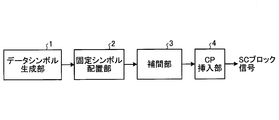
- FIG. 1 is a diagram illustrating a functional configuration example of a first embodiment of a transmission device according to the present invention.
- the transmission apparatus according to the present embodiment includes a data symbol generation unit 1, a fixed symbol arrangement unit (symbol arrangement unit) 2, an interpolation unit 3, and a CP insertion unit 4.
- the data symbol generator 1 generates data symbols (for example, PSK (Phase Shift Keying) symbols, QAM (Quadrature Amplitude Modulation) symbols, etc.).
- the fixed symbol arrangement unit 2 arranges predetermined fixed symbols at predetermined positions between data symbols to generate block symbols (symbols for one block composed of data symbols and fixed symbols).
- the interpolation unit 3 once converts the data symbols after the fixed symbol arrangement into frequency domain signals, and then converts them again into time domain signals.
- the CP insertion unit 4 inserts a CP into the time domain signal converted by the interpolation unit 3.
- the signal after CP insertion is transmitted as an SC block signal (block signal). 1 block symbol holds the N symbol, one frame is set to true by N F block symbols.
- FIG. 2 is a diagram illustrating an example in which the phase and amplitude between SC blocks are discontinuous in conventional SC block transmission.
- an out-of-band spectrum or out-of-band leakage occurs between the kth (k is an integer) th block and the (k + 1) th block.
- Such an out-of-band spectrum becomes interference of adjacent channels.
- the out-of-band spectrum is reduced by inserting fixed symbols between data symbols.
- N is an integer of 1 or more
- the data symbol generator 1 outputs N ⁇ x data symbols for each block.
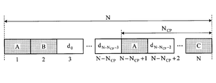
- FIG. 3 is a diagram illustrating an example of CP insertion according to the present embodiment.
- the CP insertion unit 4 copies the next N CP symbols among the input N symbols and inserts them before the N symbols.
- the horizontal axis indicates time
- L indicates an oversampling rate described later of the time domain signal output from the interpolation unit 3.
- FIG. 4 is a diagram illustrating an arrangement example of the fixed symbols A according to the present embodiment.
- x 2
- a fixed symbol A is inserted at the first and NN CP +1 symbol positions of the data symbols in one block.
- FIG. 5 is a diagram illustrating an example of a fixed symbol when a QPSK symbol is used as a data symbol.
- a data symbol is assigned to one of the four points shown as the QPSK constellation shown in the upper part of FIG. 5 according to the information to be transmitted.
- the 1st symbol and the NN CP + 1st symbol become fixed symbols and are fixed at 1 + j.
- the same fixed symbol is arranged at the same position in this way. There are no restrictions on the fixed symbols, and the present invention is not limited to the example of FIG.
- the fixed symbol indicates a symbol whose phase and amplitude are fixed, but a symbol in a specific quadrant may be used.
- two fixed symbols are inserted per block, but the number of fixed symbols is not limited to this.
- fixed symbols having the same or similar phase and amplitude are arranged in the first symbol and the NN CP + 1st symbol.
- FIG. 6 is a diagram illustrating another example of the fixed symbol according to the present embodiment. As shown in FIG. 6, a plurality of types of fixed symbols A, B, and C may be inserted. As shown in FIG. 6, an out-of-band spectrum suppression effect can be obtained by inserting a fixed symbol at the end of a block symbol.
- the interpolation unit 3 uses, for example, a signal interpolation formula described in “B. Porat,“ A Course in Digital Signal Processing ”, John Wiley and Sons Inc., 1997” (hereinafter referred to as the Porat document).
- An oversampling process (a process of increasing the sampling rate, that is, reducing the sampling interval) is performed. Oversampling is performed on the time domain signal input to the interpolation unit 3 so that there are L sampling points per symbol. That is, oversampling is performed so that the sampling rate is L times the input.
- the oversampling rate is a value indicating how many times the sampling rate after oversampling is higher than the input sampling rate.
- the interpolation unit 3 converts an input time domain signal into a frequency domain signal, performs zero insertion processing for inserting zeros into the frequency domain signal, and converts the signal into a time domain signal again. To do.
- oversampling processing can be performed using zero insertion processing.
- the oversampling process (interpolation process) in the interpolation unit 3 may use other interpolation methods. A method of performing interpolation (oversampling) without changing to a frequency domain signal may be used.
- the number of samples of the time domain signal output from the interpolation unit 3 is N ⁇ L, and the number of samples of the signal after CP insertion is (N + N CP ) ⁇ L.
- FIG. 7 is a diagram illustrating a configuration example of the interpolation unit 3 according to the present embodiment.
- the data symbol generation unit 1, the fixed symbol arrangement unit 2, and the CP insertion unit 4 shown in FIG. 7 are the same as the configuration example of FIG.
- the interpolation unit 3 shown in FIG. 1 includes a DFT unit (Fourier transform unit) 3-1, a waveform shaping filter 3-2, an oversampling process / IDFT (Inverse DFT) unit (inverse Fourier transform unit) 3- The example comprised by 3 is shown.
- DFT unit Frier transform unit
- IDFT Inverse DFT
- the DFT unit 3-1 performs N-point DFT processing and converts the input time domain signal into a frequency domain signal.
- the waveform shaping filter 3-2 performs a filtering process for removing signals other than the desired frequency domain from the frequency domain signal.
- this filtering processing for example, “T. S. Rappaport,” Wireless Communications “, 2 nd edition, Prentice Hall PTR, 2002” may be used processes such as Nyquist filtering that is described in.
- the filtering process is not limited to this.
- the oversampling process / IDFT unit 3-3 increases the number of samples by zero insertion or the like for the frequency domain signal after the filtering process (increase the number of samples corresponding to the oversampling rate L), and then the frequency domain signal IDFT processing is performed to generate a time domain signal.
- an oversampling processing unit that performs oversampling processing and an IDFT unit that performs IDFT processing may be provided. Since N-point DFT processing and L / N-point IDFT processing are performed using IFFT (Inverse Fast Fourier Transform) or FFT that requires a low amount of computation, N is 2 p (P is 1). It is desirable that L be an integer.
- the CP insertion unit 4 inserts a CP in the time domain and generates an SC block signal.
- the waveform shaping filter 3-2 does not change the number of samples of the signal
- the number of samples of the signal after CP insertion is (N + N CP ) ⁇ L as in the configuration example of FIG.
- sample points interpolated between symbols are added by the oversampling processing / IDFT unit 3-3. Due to the cyclic nature of the IDFT output explained in the above Porat document, the last symbol The interpolation point added after is an interpolated point between the last symbol and the first (first) symbol.
- the first symbol is a fixed symbol A
- the last sample (interpolated point) output from the oversampling / IDFT unit 3-3 has the phase and amplitude of the fixed symbol A. It has a continuously connected phase and amplitude (phase and amplitude close to the phase and amplitude of the fixed symbol A).
- phase and amplitude phase and amplitude close to the phase and amplitude of the fixed symbol A.
- the NN CP + 1st symbol is also the fixed symbol A
- the first symbol of the SC block output from the CP insertion unit 4 is the fixed symbol A.
- the arrangement of fixed symbols is common to all blocks, and the phase and amplitude of the last sample of the SC block and the first sample (fixed symbol) of the next SC block are smoothly connected. Therefore, continuity of phase and amplitude between blocks is maintained, and out-of-band spectrum suppression can be achieved.
- FIG. 8 is a diagram showing the relationship between the input and output of the DFT unit 3-1.
- FIG. 8 shows an example of input and output signals to the DFT unit 3-1, assuming the fixed symbol arrangement of FIG.
- FIG. 9 is a diagram illustrating an example of the fixed symbol arrangement according to the present embodiment.
- FIG. 9 shows that the fixed symbol arrangement of FIG. 4 is assumed in the block, and that this symbol arrangement is performed for all blocks.
- FIG. 10 is a diagram illustrating an output example of each unit when a fixed symbol is inserted between data symbols.
- FIG. 10 is a diagram for explaining the interpolation operation of the configuration example of FIG. 7 and uses one fixed symbol for simplicity.
- FIG. 10 shows an example in which three data symbols are generated, and the fixed symbol “ ⁇ 1” is set as the second symbol by the fixed symbol arrangement unit 2.
- the waveform shaping filter 3-2 performs waveform shaping filter processing by a rectangular window.
- the CP insertion unit 4 inserts the last two samples as a CP.
- the value of the fixed symbol arrangement (second symbol) before the DFT processing matches the value of the symbol position after the IDFT output (third sample at the double oversample point).
- An interpolation point is added between the first data symbol and the previous symbol.
- the first and second symbol interpolation has been described as an example.
- the interpolation point added after the last symbol is the last symbol and the first symbol. Is to be interpolated. Therefore, if the symbol arranged at the beginning of each block (that is, the beginning of the portion inserted as a CP) and the first symbol before CP insertion are the same or close, continuity between blocks is maintained.
- phase rotation and amplitude adjustment may be added to the fixed symbols in the block.
- the operation of the oversampling processing / IDFT unit 3-3 is not limited to the operation example shown in FIG. 10, and other zero insertion processing, signal replacement processing, and IDFT processing may be used.
- the phase continuity of the first and last samples of the output signal of the oversampling processing / IDFT section 3-3 is maintained, and the desired fixed symbol is output at the specified position. As described above, phase rotation and amplitude adjustment may be applied to each fixed symbol in the block.
- the number of data symbols including a fixed symbol is N.
- N D the number of symbols in one block
- N D the number of symbols in one block
- N D the number of symbols in one block
- the data signal input to the DFT unit 3-1 is represented by the following equation (1)
- the DFT-processed signal is represented by the following equation (2)
- the zero-inserted DFT output signal is represented by the following equation (3).
- d 0 f ⁇ c 0 ⁇ 1
- d ky f ⁇ c kx ⁇ 1
- N CP N ⁇ kx
- interpolation using the cyclic nature of the IDFT output is performed.
- the interpolation point between the last symbol of each block and the first symbol after CP insertion is the last of the block. Interpolation may be performed so as to be added as samples.
- a fixed symbol is inserted at a fixed position between data blocks, and for the data after the fixed symbol insertion, the last sample of each block is the first of each block after CP insertion. Interpolation was performed so that the phase and amplitude did not become discontinuous. For this reason, the continuity of the phase and amplitude between the blocks is maintained, and the out-of-band spectrum can be suppressed.
- FIG. FIG. 11 is a figure which shows the function structural example of Embodiment 2 of the transmitter concerning this invention.
- the transmission apparatus includes a data symbol generation unit 1-1, a fixed symbol arrangement unit 2-2, a DFT unit 3-1, an oversampling process / IDFT unit 3-3, and a waveform shaping.
- a filter 3-20, a waveform shaping filter 3-21, a frequency domain upper arrangement unit 5, a pilot signal generation unit 6, and a CP insertion unit 4 are provided.
- Components having the same functions as those in the first embodiment are denoted by the same reference numerals as those in the first embodiment, and redundant description is omitted.
- the oversampling process / IDFT unit 3-3 functions as an interpolation unit.
- a pilot signal may be used for transmission path estimation and synchronization processing, and an arrangement of pilot signals and DFT-processed data symbols is performed in the frequency domain.
- pilot signals are arranged in the frequency domain.
- the pilot signal generator 6 outputs a pilot signal as a frequency domain signal and a time domain signal of the pilot signal.
- a pilot signal as a frequency domain signal is input to a waveform shaping filter 3-21 and used for multiplexing.
- a pilot signal as a time domain signal including waveform shaping processing in the time domain is input to a fixed symbol arrangement unit 2-2. Used for fixed symbol calculation.
- the data symbol generation unit 1-1 generates data symbols in the same manner as the data symbol generation unit 1 of the first embodiment, but the number of data symbols generated per block is Nx ⁇ N P (N P is The number of pilot symbols per block).
- the fixed symbol arrangement unit 2-2 generates a fixed symbol based on a pilot signal (pilot symbol) as a time domain signal and arranges the fixed symbol at a predetermined position between data symbols.
- the DFT unit 3-1 performs DFT processing on the symbol output from the fixed symbol arrangement unit 2-2, converts the symbol into a frequency domain signal, and inputs the frequency domain signal to the waveform shaping filter 3-20.
- the waveform shaping filter 3-20 performs waveform shaping in the frequency domain on the input from the DFT unit 3-1, and outputs the processed signal to the frequency domain arrangement unit 5. Further, the waveform shaping filter 3-21 performs waveform shaping on the pilot signal as the frequency domain signal, and outputs the processed signal to the frequency domain arrangement unit 5.
- the frequency domain upper arrangement unit 5 arranges the frequency domain data symbols and fixed symbols output from the waveform shaping filter 3-20 and the frequency domain pilot signal output from the waveform shaping filter 3-21 in the frequency domain. And output to the oversampling process / IDFT unit 3-3.
- Oversampling processing / IDFT unit 3-3 performs oversampling processing and IDFT processing on the signal output from frequency domain arrangement unit 5 in the same manner as in the first embodiment, and outputs the result to CP insertion unit 4.
- the CP insertion unit 4 performs CP insertion processing on the input signal as in the first embodiment.
- FIG. 12 is a diagram showing an arrangement example of data symbols (including fixed symbols) and pilot signals under the above conditions.
- S 0, s 1, s 2 in Figure 12 ..., s N / 2-1 indicates the data symbols in the frequency domain (including a fixed symbol)
- p 0, p 1, p 2, ..., p N / 2-1 indicates a pilot signal.
- data symbols (including fixed symbols) and pilot signals are alternately arranged.
- FIG. 12 is an example, and the arrangement position and the number of pilot signals are not limited to the example of FIG.
- IDFT output time domain signal after IDFT processing by the oversampling / IDFT unit 3-3
- the pilot signal time domain signals are q 0, q 1, q 2, ...
- k ′ is a fixed symbol insertion position in the time domain
- b k ′ and c k ′ are predetermined IDFT output
- the values of b k ′ and c k ′ are determined by the pilot signal insertion position and fixed symbol arrangement position in the frequency domain.
- the time domain signal of the pilot signal is generated based on the arrangement position of the pilot signal.
- the pilot signal multiplexed in the frequency domain and the data signal to which DFT processing is added are expressed by the following formula (12), and the time domain signal is expressed by the following formula (13).
- N D + N T N, but when N D + N T ⁇ N, the same design method as in the first embodiment may be used to input a fixed signal in consideration of the time domain pilot signal. .
- N D N T
- the data symbol to which the pilot and DFT processing in the frequency domain are added is represented by the following equation (24)
- the DFT-processed signal is represented by the following equation (25). If 0 (bold) N is a vector composed of N zeros, the arrangement of pilot signals and data symbols in the frequency domain is expressed by the following equations (26) and (27), respectively.
- the time domain signal is expressed by the following formula (28), and the pilot symbol in the time domain is expressed by the following formula (29).
- the pilot signal multiplexed in the frequency domain and the data signal to which DFT processing is added are expressed by the following formula (30), and the time domain signal is expressed by the following formula (31).
- the value of fixed symbol A k ′ changes depending on the insertion position of the pilot signal or fixed symbol, and thus the above processing is performed for each block.
- a fixed insertion position of the pilot signal and the fixed symbols among the blocks once 'to previously obtain a subsequent A k already calculated' A k may be used.
- FIG. 13 is a diagram showing a specific arrangement example of data symbols and fixed symbols in the time domain when the number of pilot signal symbols is N / 2.
- the fixed symbol arrangement unit 2-2 arranges fixed symbols as shown in FIG.
- FIG. 14 is a diagram showing an example of the relationship between the input and output of the DFT unit 3-1 in the present embodiment.
- FIG. 15 is a diagram illustrating an example of the fixed symbol arrangement according to the present embodiment.
- FIG. 15 shows that the fixed symbol arrangement of FIG. 13 is assumed in the block, and that this symbol arrangement is performed for all blocks.
- the phase rotation or the fixed signal may be added to the fixed signal.
- FIG. 16 is a diagram illustrating an example of fixed symbol arrangement when a block including a pilot signal and a block not including the pilot signal coexist. In this case, in the configuration of the transmission apparatus shown in FIG.
- data symbol generation unit 1-1 and fixed symbol arrangement unit 2-2 function as data symbol generation unit 1 and fixed symbol arrangement unit 2 in Embodiment 1.
- the data symbol generation unit 1-1 and the fixed symbol arrangement unit 2-2 may operate in the same manner as in the first embodiment.
- the frequency domain arrangement unit 5 performs oversampling / IDFT unit 3-3 on the frequency domain data symbols and fixed symbols output from the waveform shaping filter 3-20 as they are. To the output.
- FIG. 17 is a diagram illustrating a configuration example of a transmission apparatus when pilot signals are multiplexed in the time domain.
- the pilot signal generation unit 6 generates a pilot signal as a time domain signal, and inputs the pilot signal to the fixed symbol arrangement unit 2-2 as in the configuration example of FIG.
- the fixed symbol arrangement unit 2-2 arranges fixed symbols as in the configuration example of FIG. 11, and outputs the data symbols and fixed symbols to the frequency / time domain conversion processing unit 7.
- the frequency / time domain conversion processing unit 7 converts the input symbol into the frequency domain, and converts it again into a time domain signal after the oversampling process. Then, the time domain multiplexing unit 8 multiplexes the output from the frequency / time domain conversion processing unit 7 and the pilot signal as the time domain signal and inputs the multiplexed signal to the CP insertion unit 4. For example, when the time domain multiplexing unit 8 uses s k as the time domain signal output from the frequency / time domain conversion processing unit 7 and q k as the pilot signal in the time domain, the time domain multiplexing signal y k becomes y. You may obtain
- require as k sk + qk.
- the fixed symbol after the pilot signals are multiplexed is set to a predetermined value at a predetermined position based on the pilot signal arrangement position.
- the fixed symbol arrangement unit 2-2 calculates the fixed symbols. For this reason, even when pilot signals are multiplexed, the continuity of phase and amplitude between blocks is maintained, and the out-of-band spectrum can be suppressed.
- FIG. 18 is a diagram illustrating a functional configuration example of the third embodiment of the transmission apparatus according to the present invention.
- the transmission apparatus of the present embodiment includes a data symbol generation unit 1-2 instead of the data symbol generation unit 1, and a quadrant mapping unit (symbol allocation unit) instead of the fixed symbol arrangement unit 2.
- a quadrant mapping unit symbol allocation unit
- 9 is the same as the configuration example of FIG.
- Components having the same functions as those in the first embodiment are denoted by the same reference numerals as those in the first embodiment, and redundant description is omitted.
- the example in which the fixed symbol is arranged at the predetermined position has been described.
- the fixed symbol not the fixed symbol but the symbol (hereinafter, referred to as a signal point in the same quadrant in the complex plane (IQ plane)).
- IQ plane complex plane
- the data symbol generation unit 1-2 generates N data symbols per block. However, among the N data symbols, data of a smaller number of bits (corresponding to lower-order data bits described later) is assigned to x symbols used as the same quadrant symbols.
- the data symbol generation unit 1-2 generates the same quadrant symbol by mapping the same quadrant symbol among the N data symbols so as to be in the same quadrant.
- the same quadrant mapping unit 9 generates a block symbol by arranging the same quadrant symbol at a predetermined position in the same manner as the fixed symbol of the first embodiment (one block symbol composed of a data symbol and the same quadrant symbol). .
- the mapping of the same quadrant symbol (generation of the same quadrant symbol) may be performed by the same quadrant mapping unit 9 by acquiring data bits from the data symbol generation unit 1-2.
- FIG. 19 is a diagram illustrating an example of the same quadrant mapping in the present embodiment.
- the first symbol A (i) and the NN CP +1 symbol B (i) are not necessarily the same, but A (i) and B (i) are in the same quadrant.
- a (i) and B (i) are mapped so as to be in the same quadrant between the blocks even though the symbols are not necessarily the same.
- data bits are not included, but in the present embodiment, data bits can be included in the same quadrant symbol, and data loss can be minimized.
- FIG. 20 is a diagram illustrating an example of the same quadrant mapping in the case of 64QAM.
- FIG. 20 shows a 64QAM constellation and a 6-bit value mapped to each point.
- a (i) and B (i) may be selected and mapped from the upper right quadrant.
- the first 2 bits of A (i) and B (i) are fixed to “00”, and the remaining lower 4 bits are arbitrary values.
- the lower 4 bits of A (i) and B (i) can be used as data bits.
- mapping processing is performed on all blocks so that the upper 2 bits of A (i) and B (i) are “00”.
- FIG. 20 shows an example in which A (i) and B (i) are mapped in the upper right quadrant.
- the present invention is not limited to this, and mapping is performed in any of the lower right, upper left, and lower left quadrants. It may be.
- FIG. 21 is a diagram illustrating an example of a symbol value when 64QAM same-quadrant mapping is performed.
- the upper 2 bits of the first and NN CP + 1st symbols are fixed to “11”.
- processing for fixing the upper 2 bits of the first and NN CP +1 symbols to “11” is performed.
- the number of data bits per block is 6N-4 bits.
- FIG. 22 is a diagram illustrating an example in which A (i) and B (i) are mapped within a predetermined range of one quadrant.
- a (i) and B (i) are mapped within a range including four signal points surrounded by dotted lines. That is, mapping may be performed so that the upper 4 bits of A (i) and B (i) are “0000”, and the lower 2 bits are data bits.
- mapping may be performed so that the upper 4 bits of A (i) and B (i) are “0000”, and the lower 2 bits are data bits.
- the description has been given using 64QAM, but any modulation method may be used.
- a k ′ (i) ′ c so that A (i) becomes the same quadrant symbol when k ′ is the same quadrant symbol insertion position as in the second embodiment.
- a symbol may be created by considering the pilot component as k ′ A (i) ⁇ b k ′ q k ′ .
- the operations of the present embodiment other than those described above are the same as those of the first embodiment.
- the fixed symbol of the first embodiment is one of the same quadrant symbols, and an example in which the predetermined range is narrowed to include only one signal point within the predetermined range can be considered.
- two symbols in the block are the same quadrant symbols, but three or more symbols may be set as the same quadrant symbols.
- phase rotation and amplitude adjustment may be performed on A (i) and B (i) so that the out-of-band spectrum is reduced.
- symbols in the same quadrant or a certain range symbols in which some bit values of all bits of the symbols are fixed values are used. Interpolation was performed as in 1. For this reason, the continuity of the phase and amplitude between blocks is maintained, the out-of-band spectrum can be suppressed, and data loss can be reduced.
- FIG. 23 is a diagram illustrating a functional configuration example of the fourth embodiment of the receiving device according to the present invention.
- the receiving apparatus according to the present embodiment receives the SC block signal transmitted by the transmitting apparatus described in the first and second embodiments.
- the synchronization processing unit 12 performs synchronization processing such as frame synchronization, frequency synchronization, symbol synchronization, and the like on the received signal (SC block signal).
- CP removing section 13 performs CP removal on the received signal after the synchronization processing.
- the DFT unit 14 performs DFT processing on the received signal from which the CP has been removed.
- the transmission path estimation unit 16 performs transmission path estimation based on the signal after DFT processing.
- the sampling processing unit 15 performs downsampling processing on the signal after DFT processing.
- the FDE unit (equalization processing unit) 17 performs FDE (Frequency Domain Equalizer) processing based on the downsampled signal and the transmission path estimation result.
- the IDFT unit 18 performs IDFT processing on the signal after the FDE processing.
- the fixed symbol removing unit 19 removes fixed symbols from the signal after the IDFT processing.
- the demodulation / decoding unit 20 performs demodulation / decoding processing on the signal after the fixed symbol is removed.
- FIG. 24 is a diagram illustrating an example in which the first symbol of the next block is CP.
- the receiving apparatus that receives the SC block signal transmitted by the transmitting apparatus described in the first and second embodiments is shown.
- the received signal is demodulated and decoded.
- FIG. FIG. 25 is a diagram illustrating an example of a functional configuration of the receiving apparatus according to the fifth embodiment of the present invention.
- the receiving apparatus according to the present embodiment receives the SC block signal transmitted by the transmitting apparatus described in the third embodiment.
- the receiving apparatus is different from the fixed symbol removing unit 19 and the demodulation / decoding unit 20 in that a demodulation / decoding / quadrant demapping unit (demodulation decoding processing unit) 19-1 is provided in the fourth embodiment. This is the same as the receiving apparatus. Components having the same functions as those in the fourth embodiment are denoted by the same reference numerals as those in the fourth embodiment, and redundant description is omitted.
- the demodulation / decoding / similar quadrant demapping unit 19-1 Based on the signal after the IDFT processing is performed by the IDFT unit 18, the demodulation / decoding / similar quadrant demapping unit 19-1 removes the fixed bits and removes the remaining fixed bits from the same quadrant symbols. Treat as data bits and perform decryption. For data symbols other than the same quadrant symbols, demodulation / decoding processing is performed as in the fourth embodiment.
- the receiving apparatus that receives the SC block signal transmitted by the transmitting apparatus described in the third embodiment is shown.
- this receiving apparatus a downsampling process is performed, and for a quadrant symbol, fixed bits are removed, and the remainder from which fixed bits are removed is treated as data bits to perform demodulation and decoding.
- the signal transmitted by the transmission apparatus described in Embodiment 3 can be demodulated and decoded.
- a guard interval other than the CP may be used.
- the data symbol and the guard interval may be arranged so that the fixed symbol (or the same quadrant symbol) is the beginning of the guard interval.
- Embodiment 6 FIG. Next, a transmission apparatus according to the sixth embodiment will be described.
- the first embodiment an example in which a plurality of types of fixed symbols are used has been described.
- a method for arranging fixed symbols that further suppresses out-of-band spectrum will be described as an extension thereof.
- FIG. 26 is a diagram illustrating an arrangement example of fixed symbols according to the present embodiment.
- blank portions where no characters are written indicate data symbols, and F i indicates a fixed symbol.
- N L + N R +1 out of N symbols in one block are fixed symbols.
- N R is X CP (X CP is the number of symbols corresponding to the portion copied as CP from the back.
- X CP N CP (CP The number of symbols to be copied)) indicates the number of continuous fixed symbols on the right side (rear side) with reference to the second, and N L is the number of fixed symbols on the left side of the reference.
- this N L + N R +1 fixed symbols are referred to as fixed symbol sequences.
- the fixed symbol sequence [F -NL, F -NL + 1 , F -NL + 2, ..., F -1, F 0, F 1, ..., F NR] denoted.
- NL and NR in the subscript indicate N L and N R , respectively.
- F i may use symbols such as M-PSK (M-ary-Phase Shift Keying) and M-QAM (M-ary Quadrature Amplitude Modulation), and some of F i may be zero. It may be set to. Further, a sequence described in “D. C. Chu,“ Polyphase Codes With Good Periodic Correlation Properties ”, IEEE Transactions on Information Theory, pp. 531-532, July 1972” may be used as a fixed symbol sequence.
- the same fixed symbol sequence is used in all blocks, and the same fixed symbols are arranged at the same position between blocks.
- the arrangement method of the fixed symbol series is as follows. F 0 of the fixed symbol series is arranged at the first position in the block and the X CP- th position from the back (N ⁇ X CP + 1-th position). Based on these positions, the order of the fixed symbol series is [F -NL , F -NL + 1 , F -NL + 2 , ..., F -1 , F 0 , F 1 , ..., F NR ].
- the fixed symbols are arranged on the left and right of the reference position so as to be arranged without changing the relative order as shown in FIG.
- F 0 is arranged at the NX CP + 1st position from the head in the block, and this F 0 position is taken as a reference position, and F 0 is continuous to the right of this reference position.
- [F 1 ,..., F NR ] and [F ⁇ NL , F ⁇ NL + 1 , F ⁇ NL + 2 ,..., F ⁇ 1 ] (first symbol group) ) Is arranged.
- F 0 is arranged at the first fixed symbol in the block, and [F 0 , F 1 ,..., F NR ] (second) after F 0 of the reference position (on the right side of the reference position and the reference position). Symbol group) is arranged.
- the part copied as CP is added before the first fixed symbol in FIG.
- the fixed symbols are arranged so that the last N L fixed symbols of the block signal are [F ⁇ NL , F ⁇ NL + 1 , F ⁇ NL + 2 ,..., F ⁇ 1 ].
- the first position in FIG. 26 is used as a reference position, and [F 1 ,..., F NR ] are arranged on the right side of this reference position in succession to F 0.
- [F ⁇ NL , F ⁇ NL + 1 , F ⁇ NL + 2 ,..., F ⁇ 1 ] are arranged.
- the interpolation point added after the last symbol is the last symbol.
- the point is to interpolate between F ⁇ 1 and the first (first) symbol F 0 .
- the head of the block signal after CP insertion is NX CP + 1st fixed symbol F 0 from the head of FIG. 26, the continuity of the phase and amplitude between the blocks can be maintained, and the out-of-band spectrum Can be suppressed. Further, by increasing N L and N R , further out-of-band spectrum suppression effect can be obtained.
- FIG. 27 is a diagram illustrating a specific example of the arrangement of fixed symbol sequences according to the present embodiment.
- FIG. 28 is a diagram showing another specific example of the arrangement of fixed symbol sequences according to the present embodiment.
- N-X CP, N -X CP + 1, N-X CP +2 th, and N are arranged fixed symbol sequence to 1, the second position.
- phase rotation is applied to the output symbol, but phase rotation may be applied to the fixed symbol sequence so that a desired phase appears in the time domain.
- FIG. 29 is a diagram illustrating a configuration example and a processing example of the transmission apparatus according to the present embodiment.
- the example of FIG. 29 is configured to include a zero insertion unit 3-4 and an IDFT unit 3-5 in place of the oversampling processing / IDFT unit 3-3, compared to the configuration example of FIG. 7 of the first embodiment.
- the waveform shaping filter 3-2 is omitted for simplification of the drawing, but a waveform shaping filter 3-2 may be provided.
- Data symbol generation unit 1, fixed symbol arrangement unit 2, CP insertion unit 4 and DFT unit 3-1 are the same as those in the first embodiment, but fixed symbol arrangement unit 2 uses the fixed symbol sequence described in the present embodiment. Generate and place As an example, FIG.
- FIG. 29 shows an example of performing interpolation by zero insertion and IDFT, and outputs [s 0 , s 1 ,... s N-1 ] is divided into two, and the zero insertion unit 3-4 inserts zeros (between s N / 2-1 and s N / 2 ) (N ⁇ (L ⁇ 1) zeros are inserted).
- L indicates the magnification in oversampling as in the first embodiment.
- the zero insertion method is the same as in the first embodiment.
- the IDFT unit 3-5 performs IDFT processing on the data after zero insertion.
- N ⁇ L signals [s 0 , s 1 ,..., S N / 2-1 , 0, 0,. , 0, s N / 2 , s N / 2 + 1 ,..., S N-1 ] are output.
- x N L + N R +1.
- FIG. 30 is a diagram illustrating another processing example of the transmission device according to the present embodiment.
- the configuration of the transmission apparatus in FIG. 30 is the same as the example in FIG. In the example of FIG. 30, a configuration example is shown in which the number of data points N D on which DFT is performed is larger than the number N of symbols in one block.
- the DFT unit 3-1 performs D- point DFT processing.
- N D point DFT processing for example, zero insertion or the like is performed in order to convert N data points to N D data, but there is no limitation on the D D point DFT processing method.
- the output from the DFT unit 3-1 is [s 0 , s 1 ,..., S ND-1 ].
- the fixed symbol series is the same between the blocks.
- the fixed symbol series may be configured to be the same quadrant symbol.
- the symbol arrangement example of FIG. 28 is used.
- the first two bits of the symbol number N ⁇ X CP and symbol number N are fixed to “00”
- pilot symbols are multiplexed as described in the second embodiment, the fixed symbol sequence of the present embodiment may be used.
- the same fixed symbol sequence is arranged in each block before and after the first position of the block symbol and the beginning of the portion copied by CP insertion as the reference position. I did it. For this reason, the continuity of the phase and amplitude between blocks can be maintained, and an out-of-band spectrum can be suppressed.
- the transmission device, the reception device, and the communication system according to the present invention are useful for a communication system that performs SC block transmission, and are particularly suitable for a communication system that performs CP insertion.
Landscapes
- Engineering & Computer Science (AREA)
- Computer Networks & Wireless Communication (AREA)
- Signal Processing (AREA)
- Physics & Mathematics (AREA)
- Discrete Mathematics (AREA)
- General Physics & Mathematics (AREA)
- Mathematical Physics (AREA)
- Spectroscopy & Molecular Physics (AREA)
- Digital Transmission Methods That Use Modulated Carrier Waves (AREA)
Abstract
Priority Applications (5)
| Application Number | Priority Date | Filing Date | Title |
|---|---|---|---|
| EP14760621.4A EP2966795B1 (fr) | 2013-03-04 | 2014-03-03 | Appareil de transmission, appareil de réception, et système de communication |
| JP2015504298A JP5951107B2 (ja) | 2013-03-04 | 2014-03-03 | 送信装置、受信装置および通信システム |
| US14/772,236 US9680681B2 (en) | 2013-03-04 | 2014-03-03 | Transmission apparatus, reception apparatus, and communication system |
| EP19188986.4A EP3584968B1 (fr) | 2013-03-04 | 2014-03-03 | Appareil de transmission |
| US15/466,189 US9866419B2 (en) | 2013-03-04 | 2017-03-22 | Transmission apparatus, reception apparatus, and communication system |
Applications Claiming Priority (2)
| Application Number | Priority Date | Filing Date | Title |
|---|---|---|---|
| JP2013041963 | 2013-03-04 | ||
| JP2013-041963 | 2013-03-04 |
Related Child Applications (2)
| Application Number | Title | Priority Date | Filing Date |
|---|---|---|---|
| US14/772,236 A-371-Of-International US9680681B2 (en) | 2013-03-04 | 2014-03-03 | Transmission apparatus, reception apparatus, and communication system |
| US15/466,189 Continuation US9866419B2 (en) | 2013-03-04 | 2017-03-22 | Transmission apparatus, reception apparatus, and communication system |
Publications (1)
| Publication Number | Publication Date |
|---|---|
| WO2014136726A1 true WO2014136726A1 (fr) | 2014-09-12 |
Family
ID=51491243
Family Applications (1)
| Application Number | Title | Priority Date | Filing Date |
|---|---|---|---|
| PCT/JP2014/055311 Ceased WO2014136726A1 (fr) | 2013-03-04 | 2014-03-03 | Appareil de transmission, appareil de réception, et système de communication |
Country Status (4)
| Country | Link |
|---|---|
| US (2) | US9680681B2 (fr) |
| EP (2) | EP3584968B1 (fr) |
| JP (1) | JP5951107B2 (fr) |
| WO (1) | WO2014136726A1 (fr) |
Cited By (6)
| Publication number | Priority date | Publication date | Assignee | Title |
|---|---|---|---|---|
| WO2015019964A1 (fr) * | 2013-08-06 | 2015-02-12 | 三菱電機株式会社 | Dispositif de transmission, dispositif de réception, et système de communication |
| WO2016136739A1 (fr) * | 2015-02-23 | 2016-09-01 | 三菱電機株式会社 | Appareil d'émission, appareil de réception et système de communication |
| JP2017157947A (ja) * | 2016-02-29 | 2017-09-07 | 三菱電機株式会社 | 送信装置、受信装置および通信システム |
| US9866419B2 (en) | 2013-03-04 | 2018-01-09 | Mitsubishi Electric Corporation | Transmission apparatus, reception apparatus, and communication system |
| JPWO2017081980A1 (ja) * | 2015-11-10 | 2018-08-23 | 三菱電機株式会社 | 送信装置、通信装置、送信信号生成方法、受信装置および復調方法 |
| JP2021530894A (ja) * | 2018-09-10 | 2021-11-11 | ミツビシ・エレクトリック・アールアンドディー・センター・ヨーロッパ・ビーヴィMitsubishi Electric R&D Centre Europe B.V. | 放出機によってサンプルのフローを受信機に転送する方法、デバイス及びコンピュータープログラム |
Families Citing this family (7)
| Publication number | Priority date | Publication date | Assignee | Title |
|---|---|---|---|---|
| EP2975790B1 (fr) | 2013-03-13 | 2019-02-20 | Mitsubishi Electric Corporation | Dispositif d'émission, dispositif de réception et système de communications |
| CN106605380B (zh) * | 2014-08-27 | 2019-05-07 | 三菱电机株式会社 | 发送装置、发送方法、接收装置以及接收方法 |
| US10454739B2 (en) * | 2015-01-23 | 2019-10-22 | Texas Instruments Incorporated | Transmission scheme for SC-FDMA with two DFT-precoding stages |
| EP3326342B1 (fr) * | 2015-07-20 | 2019-09-25 | Telefonaktiebolaget LM Ericsson (publ) | Architecture émetteur-récepteur qui soutient le temps hérité par insertion et retrait de préfixe cyclique au taux d'échantillonnage hérité |
| KR102333180B1 (ko) * | 2015-08-05 | 2021-11-30 | 삼성전자주식회사 | 플렉서블 디스플레이 장치를 구비한 전자 장치 |
| CN107370704A (zh) * | 2016-05-13 | 2017-11-21 | 财团法人工业技术研究院 | 无线通信设备及无线信号产生方法 |
| JP6735948B2 (ja) * | 2018-02-27 | 2020-08-05 | 三菱電機株式会社 | 無線送信装置、無線受信装置、無線通信システム、制御回路および記憶媒体 |
Citations (8)
| Publication number | Priority date | Publication date | Assignee | Title |
|---|---|---|---|---|
| JPH10308713A (ja) * | 1997-05-02 | 1998-11-17 | Sony Corp | 受信装置および受信方法 |
| JP2000269919A (ja) * | 1999-03-16 | 2000-09-29 | Matsushita Electric Ind Co Ltd | Ofdm通信装置 |
| JP2004201286A (ja) * | 2002-12-04 | 2004-07-15 | Matsushita Electric Ind Co Ltd | データ送信方法とデータ受信方法およびそれらを用いた送信装置と受信装置 |
| JP2007329588A (ja) * | 2006-06-06 | 2007-12-20 | Fujitsu Ltd | 送信機及び送信方法 |
| JP2008136055A (ja) * | 2006-11-29 | 2008-06-12 | Kyocera Corp | 無線通信システム、無線通信装置及び無線通信方法 |
| WO2010055639A1 (fr) * | 2008-11-13 | 2010-05-20 | パナソニック株式会社 | Appareil modulateur et procédé de modulation |
| JP2012209703A (ja) * | 2011-03-29 | 2012-10-25 | Fujitsu Semiconductor Ltd | 送信機 |
| JP2013201549A (ja) * | 2012-03-23 | 2013-10-03 | Fujitsu Semiconductor Ltd | 送信器 |
Family Cites Families (20)
| Publication number | Priority date | Publication date | Assignee | Title |
|---|---|---|---|---|
| US7106689B1 (en) | 1999-03-02 | 2006-09-12 | Matsushita Electric Industrial Co., Ltd. | OFDM transmission/reception apparatus |
| US7543009B2 (en) | 2002-12-24 | 2009-06-02 | Stmicroelectronics Belgium Nv | Fractional fourier transform convolver arrangement |
| US7680213B2 (en) | 2004-04-14 | 2010-03-16 | Nokia Corporation | Generating higher order modulation using QPSK modulations |
| BRPI0519274A2 (pt) | 2004-12-28 | 2009-01-06 | Matsushita Electric Industrial Co Ltd | aparelho de comunicaÇço sem fio e mÉtodo de comunicaÇço sem fio |
| WO2007049760A1 (fr) | 2005-10-28 | 2007-05-03 | Matsushita Electric Industrial Co., Ltd. | Dispositifs et procedes d’emission et de reception, et systeme de communication sans fil |
| TW201308928A (zh) * | 2005-12-21 | 2013-02-16 | Interdigital Tech Corp | 基魚ofdma演進utra下鏈同步頻道 |
| US7948868B2 (en) | 2006-08-18 | 2011-05-24 | Telefonaktiebolaget Lm Ericsson (Publ) | Method and arrangement relating to the insertion of pilot tones in the frequency domain in SC-FDMA |
| WO2008065901A1 (fr) | 2006-11-29 | 2008-06-05 | Kyocera Corporation | Système de communication radio, dispositif de communication radio, et procédé de communication radio |
| JP4342565B2 (ja) * | 2007-03-08 | 2009-10-14 | 株式会社東芝 | 送信機および受信機 |
| US8213538B2 (en) | 2007-05-29 | 2012-07-03 | Qualcomm Incorporated | Methods and apparatus for improved utilization of air link resources in a wireless communications system |
| EP2180603B1 (fr) | 2007-08-17 | 2015-01-21 | Panasonic Intellectual Property Corporation of America | Dispositif de communication radio et procédé de communication radio |
| JP2010041687A (ja) | 2008-08-08 | 2010-02-18 | Fujitsu Ltd | 無線通信装置および無線通信制御方法 |
| WO2010048451A2 (fr) | 2008-10-22 | 2010-04-29 | Zte (Usa) Inc. | Signalisation d'accusé de réception de liaison inverse |
| WO2011151662A1 (fr) | 2010-06-02 | 2011-12-08 | Nokia Corporation | Procédé et appareil de limitation des émissions dans les canaux adjacents en fonction d'une synchronisation de récepteur brouillé |
| JP5691380B2 (ja) | 2010-10-20 | 2015-04-01 | ソニー株式会社 | 受信装置、受信方法、およびプログラム |
| CN103004164B (zh) | 2011-05-18 | 2017-09-05 | 松下知识产权经营株式会社 | 接收装置、集成电路、接收方法及程序 |
| WO2012168926A2 (fr) * | 2011-06-10 | 2012-12-13 | Technion R&D Foundation | Récepteur, émetteur et procédé pour le traitement numérique de plusieurs sous-bandes |
| WO2013068562A1 (fr) | 2011-11-11 | 2013-05-16 | Fraunhofer-Gesellschaft zur Förderung der angewandten Forschung e.V. | Codage de partition de wedgelet efficace |
| WO2014136726A1 (fr) | 2013-03-04 | 2014-09-12 | 三菱電機株式会社 | Appareil de transmission, appareil de réception, et système de communication |
| US10299136B2 (en) | 2013-10-30 | 2019-05-21 | Mitsubishi Electric Corporation | Transmission apparatus, reception apparatus, and communication system |
-
2014
- 2014-03-03 WO PCT/JP2014/055311 patent/WO2014136726A1/fr not_active Ceased
- 2014-03-03 JP JP2015504298A patent/JP5951107B2/ja active Active
- 2014-03-03 US US14/772,236 patent/US9680681B2/en active Active
- 2014-03-03 EP EP19188986.4A patent/EP3584968B1/fr active Active
- 2014-03-03 EP EP14760621.4A patent/EP2966795B1/fr active Active
-
2017
- 2017-03-22 US US15/466,189 patent/US9866419B2/en active Active
Patent Citations (8)
| Publication number | Priority date | Publication date | Assignee | Title |
|---|---|---|---|---|
| JPH10308713A (ja) * | 1997-05-02 | 1998-11-17 | Sony Corp | 受信装置および受信方法 |
| JP2000269919A (ja) * | 1999-03-16 | 2000-09-29 | Matsushita Electric Ind Co Ltd | Ofdm通信装置 |
| JP2004201286A (ja) * | 2002-12-04 | 2004-07-15 | Matsushita Electric Ind Co Ltd | データ送信方法とデータ受信方法およびそれらを用いた送信装置と受信装置 |
| JP2007329588A (ja) * | 2006-06-06 | 2007-12-20 | Fujitsu Ltd | 送信機及び送信方法 |
| JP2008136055A (ja) * | 2006-11-29 | 2008-06-12 | Kyocera Corp | 無線通信システム、無線通信装置及び無線通信方法 |
| WO2010055639A1 (fr) * | 2008-11-13 | 2010-05-20 | パナソニック株式会社 | Appareil modulateur et procédé de modulation |
| JP2012209703A (ja) * | 2011-03-29 | 2012-10-25 | Fujitsu Semiconductor Ltd | 送信機 |
| JP2013201549A (ja) * | 2012-03-23 | 2013-10-03 | Fujitsu Semiconductor Ltd | 送信器 |
Non-Patent Citations (6)
| Title |
|---|
| B. PORAT: "A Course in Digital Signal Processing", 1997, JOHN WILEY AND SONS INC. |
| D. C. CHU: "Polyphase Codes With Good Periodic Correlation Properties", IEEE TRANSACTIONS ON INFORMATION THEORY, July 1972 (1972-07-01), pages 531 - 532, XP003015230, DOI: doi:10.1109/TIT.1972.1054840 |
| FUMIHIRO HASEGAWA: "A Novel Out-Of-Band Power Suppression Method for SC-OFDM", PROCEEDINGS OF THE 2013 IEICE GENERAL CONFERENCE TSUSHIN 1, 5 March 2013 (2013-03-05), pages 537, B-5 - 127, XP008180944 * |
| FUMIHIRO HASEGAWA: "A Novel Out-of-Band Spectrum Suppression Method without Data Loss", IEICE TECHNICAL REPORT, vol. 113, no. 194, 22 August 2013 (2013-08-22), pages 57 - 62, XP008180947 * |
| J. A. C. BINGHAM: "Multicarrier Modulation for Data Transmission: An idea Whose Time Has Come", IEEE COMMUN. MAG., vol. 28, no. 5, May 1990 (1990-05-01), pages 5 - 14, XP000132491, DOI: doi:10.1109/35.54342 |
| N. BENVENUTO; R. DINIS; D. FALCONER; S. TOMASIN: "Single Carrier Modulation With Nonlinear Frequency Domain Equalization: An Idea Whose Time Has Come-Again", PROCEEDING OF THE IEEE, vol. 98, no. 1, January 2010 (2010-01-01), pages 69 - 96, XP011286582, DOI: doi:10.1109/JPROC.2009.2031562 |
Cited By (10)
| Publication number | Priority date | Publication date | Assignee | Title |
|---|---|---|---|---|
| US9866419B2 (en) | 2013-03-04 | 2018-01-09 | Mitsubishi Electric Corporation | Transmission apparatus, reception apparatus, and communication system |
| WO2015019964A1 (fr) * | 2013-08-06 | 2015-02-12 | 三菱電機株式会社 | Dispositif de transmission, dispositif de réception, et système de communication |
| US9800445B2 (en) | 2013-08-06 | 2017-10-24 | Mitsubishi Electric Corporation | Transmission apparatus, reception apparatus, and communication system |
| WO2016136739A1 (fr) * | 2015-02-23 | 2016-09-01 | 三菱電機株式会社 | Appareil d'émission, appareil de réception et système de communication |
| JPWO2016136739A1 (ja) * | 2015-02-23 | 2017-07-13 | 三菱電機株式会社 | 受信装置 |
| US10193715B2 (en) | 2015-02-23 | 2019-01-29 | Mitsubishi Electric Corporation | Transmission apparatus, reception apparatus, and communication system |
| JPWO2017081980A1 (ja) * | 2015-11-10 | 2018-08-23 | 三菱電機株式会社 | 送信装置、通信装置、送信信号生成方法、受信装置および復調方法 |
| JP2017157947A (ja) * | 2016-02-29 | 2017-09-07 | 三菱電機株式会社 | 送信装置、受信装置および通信システム |
| JP2021530894A (ja) * | 2018-09-10 | 2021-11-11 | ミツビシ・エレクトリック・アールアンドディー・センター・ヨーロッパ・ビーヴィMitsubishi Electric R&D Centre Europe B.V. | 放出機によってサンプルのフローを受信機に転送する方法、デバイス及びコンピュータープログラム |
| JP7145987B2 (ja) | 2018-09-10 | 2022-10-03 | ミツビシ・エレクトリック・アールアンドディー・センター・ヨーロッパ・ビーヴィ | 放出機によってサンプルのフローを受信機に転送する方法、デバイス及びコンピュータープログラム |
Also Published As
| Publication number | Publication date |
|---|---|
| EP2966795B1 (fr) | 2019-11-13 |
| US9866419B2 (en) | 2018-01-09 |
| EP2966795A1 (fr) | 2016-01-13 |
| US20160013963A1 (en) | 2016-01-14 |
| US9680681B2 (en) | 2017-06-13 |
| EP3584968A1 (fr) | 2019-12-25 |
| US20170195156A1 (en) | 2017-07-06 |
| JPWO2014136726A1 (ja) | 2017-02-09 |
| EP3584968B1 (fr) | 2023-09-13 |
| JP5951107B2 (ja) | 2016-07-13 |
| EP2966795A4 (fr) | 2017-01-04 |
Similar Documents
| Publication | Publication Date | Title |
|---|---|---|
| JP5951107B2 (ja) | 送信装置、受信装置および通信システム | |
| JP6918157B2 (ja) | 送信装置 | |
| JP6026006B2 (ja) | 送信装置、受信装置および通信システム | |
| JP6025987B2 (ja) | 送信装置、受信装置および通信システム | |
| JP6214822B2 (ja) | 送信装置、受信装置および通信システム | |
| WO2016031496A1 (fr) | Appareil de transmission, procédé de transmission, appareil de réception et procédé de réception |
Legal Events
| Date | Code | Title | Description |
|---|---|---|---|
| 121 | Ep: the epo has been informed by wipo that ep was designated in this application |
Ref document number: 14760621 Country of ref document: EP Kind code of ref document: A1 |
|
| ENP | Entry into the national phase |
Ref document number: 2015504298 Country of ref document: JP Kind code of ref document: A |
|
| WWE | Wipo information: entry into national phase |
Ref document number: 14772236 Country of ref document: US |
|
| NENP | Non-entry into the national phase |
Ref country code: DE |
|
| WWE | Wipo information: entry into national phase |
Ref document number: 2014760621 Country of ref document: EP |