WO2014136882A1 - Dispositif de source de lumière et projecteur - Google Patents
Dispositif de source de lumière et projecteur Download PDFInfo
- Publication number
- WO2014136882A1 WO2014136882A1 PCT/JP2014/055794 JP2014055794W WO2014136882A1 WO 2014136882 A1 WO2014136882 A1 WO 2014136882A1 JP 2014055794 W JP2014055794 W JP 2014055794W WO 2014136882 A1 WO2014136882 A1 WO 2014136882A1
- Authority
- WO
- WIPO (PCT)
- Prior art keywords
- light
- wavelength
- light quantity
- band
- measuring means
- Prior art date
- Legal status (The legal status is an assumption and is not a legal conclusion. Google has not performed a legal analysis and makes no representation as to the accuracy of the status listed.)
- Ceased
Links
Images



Classifications
-
- H—ELECTRICITY
- H04—ELECTRIC COMMUNICATION TECHNIQUE
- H04N—PICTORIAL COMMUNICATION, e.g. TELEVISION
- H04N9/00—Details of colour television systems
- H04N9/12—Picture reproducers
- H04N9/31—Projection devices for colour picture display, e.g. using electronic spatial light modulators [ESLM]
- H04N9/3141—Constructional details thereof
- H04N9/315—Modulator illumination systems
- H04N9/3155—Modulator illumination systems for controlling the light source
-
- G—PHYSICS
- G03—PHOTOGRAPHY; CINEMATOGRAPHY; ANALOGOUS TECHNIQUES USING WAVES OTHER THAN OPTICAL WAVES; ELECTROGRAPHY; HOLOGRAPHY
- G03B—APPARATUS OR ARRANGEMENTS FOR TAKING PHOTOGRAPHS OR FOR PROJECTING OR VIEWING THEM; APPARATUS OR ARRANGEMENTS EMPLOYING ANALOGOUS TECHNIQUES USING WAVES OTHER THAN OPTICAL WAVES; ACCESSORIES THEREFOR
- G03B21/00—Projectors or projection-type viewers; Accessories therefor
- G03B21/14—Details
- G03B21/20—Lamp housings
- G03B21/2006—Lamp housings characterised by the light source
- G03B21/2033—LED or laser light sources
-
- G—PHYSICS
- G03—PHOTOGRAPHY; CINEMATOGRAPHY; ANALOGOUS TECHNIQUES USING WAVES OTHER THAN OPTICAL WAVES; ELECTROGRAPHY; HOLOGRAPHY
- G03B—APPARATUS OR ARRANGEMENTS FOR TAKING PHOTOGRAPHS OR FOR PROJECTING OR VIEWING THEM; APPARATUS OR ARRANGEMENTS EMPLOYING ANALOGOUS TECHNIQUES USING WAVES OTHER THAN OPTICAL WAVES; ACCESSORIES THEREFOR
- G03B21/00—Projectors or projection-type viewers; Accessories therefor
- G03B21/14—Details
- G03B21/20—Lamp housings
- G03B21/208—Homogenising, shaping of the illumination light
-
- G—PHYSICS
- G03—PHOTOGRAPHY; CINEMATOGRAPHY; ANALOGOUS TECHNIQUES USING WAVES OTHER THAN OPTICAL WAVES; ELECTROGRAPHY; HOLOGRAPHY
- G03B—APPARATUS OR ARRANGEMENTS FOR TAKING PHOTOGRAPHS OR FOR PROJECTING OR VIEWING THEM; APPARATUS OR ARRANGEMENTS EMPLOYING ANALOGOUS TECHNIQUES USING WAVES OTHER THAN OPTICAL WAVES; ACCESSORIES THEREFOR
- G03B33/00—Colour photography, other than mere exposure or projection of a colour film
- G03B33/06—Colour photography, other than mere exposure or projection of a colour film by additive-colour projection apparatus
-
- H—ELECTRICITY
- H01—ELECTRIC ELEMENTS
- H01S—DEVICES USING THE PROCESS OF LIGHT AMPLIFICATION BY STIMULATED EMISSION OF RADIATION [LASER] TO AMPLIFY OR GENERATE LIGHT; DEVICES USING STIMULATED EMISSION OF ELECTROMAGNETIC RADIATION IN WAVE RANGES OTHER THAN OPTICAL
- H01S5/00—Semiconductor lasers
- H01S5/06—Arrangements for controlling the laser output parameters, e.g. by operating on the active medium
- H01S5/068—Stabilisation of laser output parameters
- H01S5/0683—Stabilisation of laser output parameters by monitoring the optical output parameters
-
- H—ELECTRICITY
- H04—ELECTRIC COMMUNICATION TECHNIQUE
- H04N—PICTORIAL COMMUNICATION, e.g. TELEVISION
- H04N9/00—Details of colour television systems
- H04N9/12—Picture reproducers
- H04N9/31—Projection devices for colour picture display, e.g. using electronic spatial light modulators [ESLM]
- H04N9/3179—Video signal processing therefor
- H04N9/3182—Colour adjustment, e.g. white balance, shading or gamut
-
- H—ELECTRICITY
- H04—ELECTRIC COMMUNICATION TECHNIQUE
- H04N—PICTORIAL COMMUNICATION, e.g. TELEVISION
- H04N9/00—Details of colour television systems
- H04N9/12—Picture reproducers
- H04N9/31—Projection devices for colour picture display, e.g. using electronic spatial light modulators [ESLM]
- H04N9/3191—Testing thereof
- H04N9/3194—Testing thereof including sensor feedback
-
- H—ELECTRICITY
- H05—ELECTRIC TECHNIQUES NOT OTHERWISE PROVIDED FOR
- H05B—ELECTRIC HEATING; ELECTRIC LIGHT SOURCES NOT OTHERWISE PROVIDED FOR; CIRCUIT ARRANGEMENTS FOR ELECTRIC LIGHT SOURCES, IN GENERAL
- H05B45/00—Circuit arrangements for operating light-emitting diodes [LED]
- H05B45/20—Controlling the colour of the light
-
- H—ELECTRICITY
- H05—ELECTRIC TECHNIQUES NOT OTHERWISE PROVIDED FOR
- H05B—ELECTRIC HEATING; ELECTRIC LIGHT SOURCES NOT OTHERWISE PROVIDED FOR; CIRCUIT ARRANGEMENTS FOR ELECTRIC LIGHT SOURCES, IN GENERAL
- H05B45/00—Circuit arrangements for operating light-emitting diodes [LED]
- H05B45/20—Controlling the colour of the light
- H05B45/22—Controlling the colour of the light using optical feedback
-
- G—PHYSICS
- G03—PHOTOGRAPHY; CINEMATOGRAPHY; ANALOGOUS TECHNIQUES USING WAVES OTHER THAN OPTICAL WAVES; ELECTROGRAPHY; HOLOGRAPHY
- G03B—APPARATUS OR ARRANGEMENTS FOR TAKING PHOTOGRAPHS OR FOR PROJECTING OR VIEWING THEM; APPARATUS OR ARRANGEMENTS EMPLOYING ANALOGOUS TECHNIQUES USING WAVES OTHER THAN OPTICAL WAVES; ACCESSORIES THEREFOR
- G03B21/00—Projectors or projection-type viewers; Accessories therefor
- G03B21/14—Details
- G03B21/20—Lamp housings
- G03B21/2053—Intensity control of illuminating light
Definitions
- the present invention relates to a light source device using light emitting elements such as semiconductor lasers of a plurality of different wavelength bands that can be used in an optical device such as a projector.
- HID lamps high-intensity discharge lamps
- TM DLP
- TM liquid crystal projectors
- photomask exposure apparatuses photomask exposure apparatuses.
- FIG. 7 is a diagram for explaining one form of a part of a conventional projector related to the projector of the present invention (reference: Japanese Patent Application Laid-Open No. 2004-252112, etc.).
- a light condensing means (not shown) composed of a concave reflecting mirror, a lens, or the like.
- FmA is input to the incident end (PmiA) and output from the exit end (PmoA).
- a light guide can be used, which is also called a name such as a rod integrator or a light tunnel, and is a light transmissive material such as glass or resin.
- the light homogenizing means (FmiA) repeats total reflection on the side surface of the light homogenizing means (FmA). FmA) so that the illuminance on the exit end (PmoA) is sufficiently uniform even if the distribution of light input to the entrance end (PmiA) is uneven. Function.
- a hollow square tube the inner surface of which is a reflecting mirror
- the illumination lens (Ej1A) is arranged so that a square image of the emission end (PmoA) is formed on the two-dimensional light amplitude modulation element (DmjA), and is output from the emission end (PmoA).
- the two-dimensional light amplitude modulation element (DmjA) is illuminated with light.
- a mirror (MjA) is arranged between the illumination lens (Ej1A) and the two-dimensional light amplitude modulation element (DmjA).
- the two-dimensional light amplitude modulation element (DmjA) modulates the light so that it is directed to the direction in which the light is incident on the projection lens (Ej2A) for each pixel or in the direction not to be incident, according to the video signal.
- An image is displayed on the screen (Tj).
- the two-dimensional light amplitude modulation element as described above is sometimes called a light valve.
- the DMD (TM) digital
- DmjA two-dimensional light amplitude modulation element
- Micromirror devices are often used.
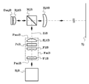
- FIG. 8 is a diagram for explaining one form of a kind (reference: Japanese Patent Application Laid-Open No. 2001-142141, etc.).
- the light from the light source (SjB) composed of a high-intensity discharge lamp or the like is made into a uniform light beam by a fly-eye integrator with the help of collimator means (not shown) composed of a concave reflecting mirror or lens.
- the light uniformizing means (FmB) is configured by a combination of an incident-side front stage fly-eye lens (F1B), an exit-side rear stage fly-eye lens (F2B), and an illumination lens (Ej1B).
- Both the front fly-eye lens (F1B) and the rear fly-eye lens (F2B) are formed by arranging a large number of rectangular lenses having the same focal length and the same shape in the vertical and horizontal directions.
- Each lens of the front-stage fly-eye lens (F1B) and the corresponding lens of the rear-stage fly-eye lens (F2B) in the subsequent stage constitute an optical system called Koehler illumination.
- a large number of optical systems are arranged vertically and horizontally.
- the Kohler illumination optical system is composed of two lenses.
- the front lens collects light and illuminates the target surface, the front lens does not form a light source image on the target surface, but the center of the rear lens.
- a light source image is formed on this surface, and the rear lens is arranged so as to form an image of the quadrangle of the outer shape of the front lens on the target surface (surface to be illuminated), thereby uniformly illuminating the target surface.
- the function of the latter lens is to prevent the phenomenon that the illuminance around the square of the target surface falls depending on the size when the light source is not a perfect point light source but has a finite size if it is not
- the rear lens can make the illuminance uniform to the periphery of the square of the target surface without depending on the size of the light source.
- the front stage fly-eye lens (F1B) and the rear stage fly-eye lens ( The distance from F2B) is set to be equal to the focal length thereof, so that an image of the target surface of uniform illumination as the Kohler illumination optical system is generated at infinity.
- the illumination lens (Ej1B) is arranged at the rear stage of the rear fly-eye lens (F2B), the target surface is drawn onto the focal plane of the illumination lens (Ej1B) from infinity.
- the output light beams are also substantially axially symmetric. Because of the nature of the lens, that is, the Fourier transform of the lens, all rays incident on the lens surface at the same angle are refracted toward the same point on the focal plane regardless of the incident position on the lens surface.
- the output of the Koehler illumination optical system is imaged on the same target surface on the focal plane of the illumination lens (Ej1B).
- a polarizing beam splitter (MjB) is disposed between the illumination lens (Ej1B) and the two-dimensional light amplitude modulation element (DmjB), so that light is transmitted to the two-dimensional light amplitude modulation element ( DmjB) is reflected.
- the two-dimensional light amplitude modulation element (DmjB) rotates the polarization direction of light by 90 degrees for each pixel according to the video signal, or modulates and reflects the light so that only the rotated light is reflected. Then, the light passes through the polarizing beam splitter (MjB) and is incident on the projection lens (Ej3B) to display an image on the screen (Tj).
- LCOS silicon liquid crystal device
- DmjB two-dimensional light amplitude modulation element
- a transmissive liquid crystal device (LCD) is also used with an optical arrangement suitable for it (reference: 10-133303).
- a dynamic color filter such as a color wheel is disposed after the light uniformizing means, and R, G, B (red and green, blue)
- the two-dimensional light amplitude modulation element is illuminated as a color sequential light beam, and color display is realized by time division, or a dichroic mirror or dichroic prism is arranged at the subsequent stage of the light uniformizing means, and R, G, B
- a dichroic mirror or dichroic prism to perform color synthesis of modulated light beams of the three primary colors R, G, and B
- the high-intensity discharge lamp described above has drawbacks such as low conversion efficiency from input power to optical power, that is, large heat loss or short life.
- solid light sources such as LEDs and semiconductor lasers have attracted attention as alternative light sources that have overcome these drawbacks.
- the LED has a smaller heat loss and a longer life than the discharge lamp, but the emitted light has no directivity like the discharge lamp.
- the light use efficiency is low.
- the semiconductor laser has a drawback that speckle is generated due to its high coherence, but it can be overcome by various technical improvements such as using a diffusion plate.
- Advantages of high light utilization efficiency even in applications where only light in a specific direction can be used, such as the projectors and exposure apparatuses described above, because of low heat loss, long life, and high directivity There is.
- the high directivity makes it possible to perform optical transmission with high efficiency, so it is possible to separate the installation location of the semiconductor laser from the location where the light is used, such as a projector. The degree of freedom can be increased.
- the emission wavelength and emission intensity of the semiconductor laser change due to a temperature increase due to environmental temperature change or self-heating and further deterioration due to an increase in accumulated energization time.
- a semiconductor laser is used as part of or all of the R, G, and B3 primary colors as the light source of the projector, the color and brightness of the entire image change due to such changes. Therefore, when applying a semiconductor laser to a high-fidelity projector, it is necessary to stabilize the color, that is, the white balance and the brightness.
- the inclination of the spectral sensitivity characteristic is a direction in which the light emission wavelength becomes longer by performing light amount detection using a positive light sensor and a negative light sensor in the light emission wavelength band of the light source. Or the direction of shortening or no change, and based on the result, the reference level of the input power control of the R, G, B color light sources is determined. The technology to increase or decrease is described.
- this technology detects and controls only the direction of temporal change in the emission wavelength, so it corrects relatively fast color changes due to temperature changes due to the heat generated by the light source itself immediately after the light source is turned on. Although it may be possible, there is a problem that it cannot cope with a very slow environmental temperature change or a color change accompanying a deterioration of a light source over a long period of time. Further, it remains unsolved how to control the input power for each color light source when multiple color light sources cause color changes independently at the same time.
- the angle of the dichroic mirror is changed based on the output from the LED light source and the detection result of the light detection sensor for detecting the color, and an inconvenient wavelength component in the light emission from the LED is detected.
- a technique for correcting the color by discarding is described, it has been low in efficiency because unnecessary light is discarded, and a method for realizing a light detection sensor for detecting a color has not been solved.
- the problem to be solved by the present invention is to quantitatively measure the hue of the output light beam using a simple filter without incorporating a high-cost chromaticity meter equipped with a filter having precise spectral characteristics.
- An object of the present invention is to provide a light source device and a projector that can maintain a target hue by back control.
- the light source device includes a light emitting element (Y1a, Y1b,%) That emits light in a narrow wavelength band and a drive circuit (P1a, P1b,%) That drives the light emitting elements (Y1a, Y1b,.
- a light source device that radiates to The light emitting elements (Y1a, Y1b,..., Y2a, Y2b,...) Include elements whose emission wavelengths belong to a plurality of different wavelength bands, Further, the light source device receives an amount of light that correlates with the amount of light of the output light beam (Fo, Fo1, Fo2,%) In order to measure the total light of the output light beam (Fo, Fo1, Fo2,).
- the control circuit (Mc) at least intermittently acquires band light characteristic measurement data generated by the band light characteristic measuring means to generate the emission intensity instruction value and the wavelength deviation instruction value, and the control circuit (Mc) generates a hue instruction value that correlates with the overall light color of the output light beam (Fo, Fo1, Fo2,%), And reduces the difference between the hue instruction value and its target value.
- the drive circuits (P1a, P1b,..., P2a, P2b,...) are feedback-controlled, and the control circuit (Mc) has the same color necessary for calculating the chromaticity when generating the hue instruction value.
- the control circuit (Mc) has the same color necessary for calculating the chromaticity when generating the hue instruction value.
- local band color matching function information consisting of the function value at the reference wavelength and the change rate of the function with respect to the wavelength change, that is, the slope of the function value change at the time of the wavelength change, for each of the wavelength bands described above
- the hue instruction value is calculated based on an amount correlated with chromaticity coordinates using the wavelength deviation instruction value and the local band color matching function information for each of the wavelength bands described above.
- the band light characteristic measuring means for at least one of the wavelength bands is a first light quantity measuring means (A1R, A1G, A1B) having a first spectral sensitivity characteristic for the spectral sensitivity characteristic of the wavelength band.
- the second light quantity measuring means (A2R, A2G, A2B) having the second spectral sensitivity characteristic, and the first spectral sensitivity characteristic and the second spectral sensitivity characteristic described above ,
- the rate of change of sensitivity with respect to wavelength change that is, the slope of the sensitivity change at the time of wavelength change is different
- the control circuit (Mc) has a sensitivity value at a reference wavelength and a sensitivity to a change in the wavelength of each of the first spectral sensitivity characteristic and the second spectral sensitivity characteristic in the wavelength band.
- the control circuit (Mc) has a first light amount measuring means (A1R, A1G, A1B) which is the band light characteristic measurement data and has local band spectral sensitivity information including a change rate.
- the first light quantity measurement data (Sh1R, Sh1G, Sh1B) and the second light quantity measurement data (Sh2R, H2G is characterized in that obtained by generating a wavelength deviation instruction value the emission intensity readings described above from the SH2B).
- the control circuit (Mc) includes the hue instruction value correlated with the overall light color of the output light beam (Fo, Fo1, Fo2,%), A brightness instruction value correlated with the overall light brightness of the output light beam (Fo, Fo1, Fo2,%) Is generated, and in addition to the difference between the hue instruction value and its target value, the brightness instruction value and its target value.
- the drive circuits (P1a, P1b,..., P2a, P2b,...) Are feedback-controlled so as to reduce the difference.
- the control circuit (Mc) determines the amount of change in the hue instruction value when the emission intensity instruction value for each of the wavelength bands is slightly changed. Using the amount of change of the emission intensity instruction value determined, a coefficient when expressed by the linear calculation is determined, and the amount of change of the emission intensity instruction value for each of the wavelength bands described above is determined via the coefficient. The above-described feedback control is performed.
- the first light quantity measuring means (A1R, A1G, A1B) and the second light quantity measuring means (A2R, A2G, A2B) are respectively optical sensors (C1R, C1G, C1B), and characteristic filters (Et1, Et2) are provided on at least one front surface of the photosensors (C1R, C1G, C1B).
- the first light quantity measuring means (A1R, A1G, A1B) and the second light quantity measuring means (A2R, A2G, A2B) are alternately arranged with respect to the same light quantity measuring means.
- the first light quantity measuring means (A1R, A1G, A1B) and the second light quantity measuring means (A2R, A2G, A2B) are optical sensors.
- a characteristic filter (Et1, Et2) different from that used as the first light quantity measuring means (A1R, A1G, A1B) is used. It is characterized by providing. *
- At least one of the optical sensors of the first light quantity measuring means (A1R, A1G, A1B) and the second light quantity measuring means (A2R, A2G, A2B) is an image sensor. It is characterized by being.
- a projector according to a seventh aspect of the present invention is characterized in that an image is projected and displayed using the light source device according to the first to sixth aspects.
- the hue of the output light beam is quantitatively measured using a simple filter without incorporating a high-cost chromaticity meter equipped with a filter having precise spectral characteristics, and a target is obtained by food back control. It is possible to provide a light source device and a projector that can maintain the hue as described above.
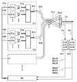
- the block diagram which simplifies and shows the light source device of this invention is represented.
- the block diagram which simplifies and shows the light source device of this invention is represented.
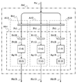
- the block diagram which simplifies and shows a part of light source device of this invention is represented.
- the schematic of the concept relevant to the technique of the light source device of this invention is represented.
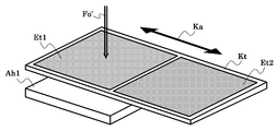
- the schematic diagram which simplifies and shows a part of light source device of this invention is represented.
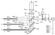
- the figure which simplifies and shows one form of the Example of the light source device of this invention is represented.
- the figure explaining one form of one part of the kind of the conventional projector concerning the projector of this invention is represented.
- the figure explaining one form of one part of the kind of the conventional projector concerning the projector of this invention is represented.
- FIG. 1 is a block diagram which simplifies and shows the light source device of this invention.
- At least one light emitting element (Y1a, Y1b,%) Provided in the element light source (U1) is driven by a drive circuit (P1a, P1b,%) To emit light.
- a drive circuit P1a, P1b, etc.
- a semiconductor laser or a radiated light of the semiconductor laser is utilized by utilizing a nonlinear optical phenomenon such as harmonic generation or an optical parametric effect.
- a light source for wavelength conversion, etc. which can be driven by one drive circuit (P1a, P1b,...) By connecting a plurality of such light sources in series, in parallel, or in series-parallel connection. It is said.
- the drive circuits (P1a, P1b,...) are DC / DC converters configured by a circuit of a system such as a step-down chopper or a step-up chopper, which is fed by a DC power supply (not shown). It is assumed that prescribed power can be input to the light emitting elements (Y1a, Y1b,).
- the control circuit (Mc) is controlled independently for each of the drive circuits (P1a, P1b,..., P2a, P2b,%) Via drive circuit control signals (J1a, J1b,..., J2a, J2b, etc.
- Each light emitting element (Y1a, Y1b,..., Y2a, Y2b,%) Can be supplied with a prescribed power.
- the light source device of the present invention has a plurality of element light sources similar to the element light source (U1), and the light emitting elements (Y1a, Y1b,..., Y2a, Y2b, etc Included therein emit light. Wavelengths belonging to a plurality of different narrow wavelength bands are included, and the included wavelength bands are the three primary colors R, G, and B here. Therefore, in order to measure the overall light characteristics of the output light beams (Fo1, Fo2,%) Of these element light sources (U1, U2,7), The output light beams (Fo1, Fo2,.
- a measurement output light beam (Fo ′, Fo ′′) consisting of an amount of light correlated with the light amount of the output light beam (Fo1, Fo2,. The light is incident on the band light characteristic measuring means provided for each.
- the total light characteristic means that the output light beams (Fo1, Fo2,%) Are mixed and output light in the wavelength bands of R, G, and B.
- image information is put on light by two-dimensional light amplitude modulation for each wavelength band, and finally, Assuming a state where all of the output light beams (Fo1, Fo2,%) Are mixed, the light content by wavelength band and the respective wavelength bands in the entire output light beam (Fo1, Fo2,%) The characteristics of the output light beam (Fo1, Fo2,%) Such as the color of the light.
- Correlation with the amount of light of the output light beam means that if the measurement output light beam (Fo ', Fo ") is measured, the light amount and hue of each of the output light beams (Fo1, Fo2, ...) are estimated. In this case, even if the correlation magnification (correlation coefficient) is different for each wavelength band, it does not matter because it can be measured and corrected in advance. There may be a difference in the correlation magnification between the measurement output light beams (Fo ′, Fo ′′).
- the band light characteristic measuring means is for measuring an emission intensity instruction value correlated with light intensity and a wavelength deviation instruction value correlated with a deviation from a reference wavelength.
- the band light characteristic measuring means for at least one of the measured wavelength bands includes a first light quantity measuring means having a first spectral sensitivity characteristic for a spectral sensitivity characteristic of the wavelength band, and a second spectral sensitivity characteristic.
- the band light characteristic measuring means having other configurations that are not as described above can be used, which will be described later.
- the measurement output light beam (Fo ′) is input to the first light quantity measuring means (A1R, A1G, A1B) provided for each of the wavelength bands described above, and the measurement is performed.
- the output light beam (Fo ′′) is input to the second light quantity measuring means (A2R, A2G, A2B) provided for each of the wavelength bands described above.
- the first light quantity measuring means (A1R, A1G, A1B) in the R, G, B wavelength bands are grouped to form a first light quantity measuring means group (Ax1), and each of the R, G, B wavelengths.
- the second light quantity measuring means (A2R, A2G, A2B) in the band are grouped and drawn as a second light quantity measuring means group (Ax2) for convenience of convenience.
- the measurement means and the second light quantity measurement means are grouped, the G color first light quantity measurement means and the second light quantity measurement means are grouped, and the B color first light quantity measurement means and the second light quantity measurement means are grouped together. You may make it group.
- the measurement output light beam (Fo ′, Fo ′′) is formed by collecting the light beams extracted one by one from the output light beam (Fo1, Fo2,...) In each wavelength band.
- the measurement output light beam for each wavelength band may be individually input to the band light characteristic measurement means for each wavelength band.
- the output light beam (Fo1, Fo2,%) Illuminates a two-dimensional light amplitude modulation element provided separately for each color of R, G, and B, and a dichroic mirror, A method of arranging the dichroic prism to synthesize the modulated light beams of the three primary colors of R, G, and B, or mixing all of the output light beams (Fo1, Fo2,%), For example, as white light. It can be used as an alternative to light from a light source (SjA) comprising a luminance discharge lamp or the like.
- FIG. 2 is a block diagram showing the light source device of the present invention in a simplified manner
- the light emitted from the light emitting elements (Y1a, Y1b,..., Y2a, Y2b,...) Is collected from, for example, a lens.
- the light is condensed on the incident ends (Ei1, Ei2,%) Of the optical fibers (Ef1, Ef2,%) By the optical optical system (Ec1, Ec2,%) And propagates through the cores of the optical fibers (Ef1, Ef2,. It is also possible to radiate from the emission ends (Eo1, Eo2,).
- the radiated light from the emission ends (Eo1, Eo2,%) Of the optical fibers (Ef1, Ef2,%) Of the element light sources (U1, U2,%) are combined into one output light beam (Fo).
- Output from the light source device As a comprehensive method of radiated light from a plurality of emission ends (Eo1, Eo2,%), The simplest method is to align the emission ends (Eo1, Eo2,%) On the same plane. This can be realized by bundling the emission ends of the optical fibers (Ef1, Ef2,). A part of the emitted light from the emission end (Eo1, Eo2,%) So that the amount correlated with the amount of the output light beam (Fo) guided by each of the optical fibers (Ef1, Ef2,%) Can be measured.
- the group (Ax1) and the second light quantity measuring means (A2R, A2G, A2B) may be input to the second light quantity measuring means group (Ax2) grouped.
- all the output ends of the optical fibers (Ef1, Ef2,...) Are bundled to generate an output light beam (Fo) of white light.
- the output ends (Eo1, Eo2,%) May be separately bundled to generate output light fluxes for each wavelength band, and each may be individually input to the band light characteristic measuring means.
- the measurement output light beam (Fo ′) is The measurement output light beam (Ft1) input to the characteristic filter (Et1) and passed therethrough passes through the R, G, B3 color band filters (Et1R, Et1G, Et1B), respectively, and the optical sensor (C1R, C1G and C1B) receive light.
- the light detection signals (Sg1R, Sg1G, Sg1B) from the photosensors (C1R, C1G, C1B) are subjected to necessary processing such as amplification and AD conversion by a light quantity measurement circuit (H1R, H1G, H1B), and R, G , B, first light quantity measurement data (Sh1R, Sh1G, Sh1B) including information on the quantity of light in each wavelength band is generated.
- the spectral sensitivity characteristics of the first light quantity measuring means (A1R, A1G, A1B) include the light caused by the characteristic filter (Et1) and the bandpass filters (Et1R, Et1G, Et1B).
- the characteristic filter (Et1) is described as being configured to provide a common one for each of the first light quantity measurement means (A1R, A1G, A1B), the first light quantity measurement means ( A1R, A1G, and A1B) may be individually provided.
- the light quantity measurement circuit (H1R, H1G, H1B) is configured to provide a separate signal for each of the light detection signals (Sg1R, Sg1G, Sg1B), a selection signal is described.
- an analog multiplexer for selecting one of the light detection signals (Sg1R, Sg1G, Sg1B) according to the above, and a common one for each of the light detection signals (Sg1R, Sg1G, Sg1B) May be.
- a characteristic filter (Et2) having a different spectral sensitivity characteristic is provided.
- An optical sensor circuit comprising the band filter (Et1R, Et1G, Et1B) of the single light quantity measuring means (A1R, A1G, A1B), the optical sensor (C1R, C1G, C1B), and the light quantity measuring circuit (H1R, H1G, H1B).
- the second light quantity measurement data (Sh2R, Sh2G, Sh2B) may be generated by using the same part (Ah1).
- the control circuit (Mc) can read the first light quantity measurement data (Sh1R, Sh1G, Sh1B) and the second light quantity measurement data (Sh2R, Sh2G, Sh2B).
- the band filter (Et1R, Et1G, Et1B) is not divided into the characteristic filter (Et1) and the bandpass filter (Et1R, Et1G, Et1B) of the first light quantity measuring means (A1R, A1G, A1B).
- Each may also be configured to have the function of the characteristic filter (Et1).
- the band filters of the second light quantity measuring means (A2R, A2G, A2B) may be transparent.
- the optical sensor when the output luminous flux (Fo1, Fo2,%) Is divided into R, G, and B colors and used independently for each color, the optical sensor ( Each of C1R, C1G, and C1B) may be configured as a separate body instead of being mounted together in the single optical sensor circuit portion (Ah1).
- the second spectral sensitivity characteristic of A2B) is only required to realize a state in which the rate of change in sensitivity with respect to a change in wavelength, that is, the slope of the change in sensitivity at the time of wavelength change is different in each wavelength band.
- the spectral sensitivity characteristic means a set of a spectral sensitivity characteristic in the R color wavelength band, a spectral sensitivity characteristic in the G color wavelength band, and a spectral sensitivity characteristic in the B color wavelength band in this case.
- the difference in sensitivity change rate with respect to wavelength change in one wavelength band is that one is positive and the other is negative, or one is substantially zero and the other is non-zero (finite value).
- the aforementioned bandwidth is usually Is only a few nanometers to about 10 nanometers, but for each of the first spectral sensitivity characteristic and the second spectral sensitivity characteristic, the change in the rate of change of sensitivity with respect to the change in wavelength within this bandwidth. It is desirable that there are few.
- the control circuit (Mc) determines the sensitivity value at the reference wavelength and the sensitivity value for each of the R, G, and B wavelength bands for each of the first spectral sensitivity characteristic and the second spectral sensitivity characteristic. Possesses local band spectral sensitivity information consisting of the rate of change of sensitivity with respect to changes in wavelength. Therefore, as will be described later, the control circuit (Mc) reads the first light quantity measurement read from the first light quantity measurement means (A1R, A1G, A1B) and the second light quantity measurement means (A2R, A2G, A2B).
- the local band spectral sensitivity information is used for each of the R, G, B wavelength bands. It is possible to approximately calculate the emission intensity instruction value correlating with the intensity and the wavelength deviation instruction value correlating with the deviation from the reference wavelength.
- the color of light emitted from a light source or the like is represented by chromaticity coordinates based on the XYZ color system that is established by CIE.
- CIE Color Engineering Laboratory
- the tristimulus values X, Y, Z of the light beam to be measured represented by the spectrum S ( ⁇ ) with the wavelength ⁇ as a parameter are the color matching functions xe ( ⁇ ), ye ( ⁇ ), ze () defined by the CIE.
- FIG. 4A is a schematic diagram of the concept related to the technology of the light source device of the present invention.
- FIG. 4A is a schematic diagram of the concept related to the technology of the light source device of the present invention. .
- the color matching function uses a symbol with a horizontal bar on each letter of x, y, z. However, in this specification, it is described as described above for convenience.
- the control circuit (Mc) determines the function value and wavelength at the reference wavelength for each of the color matching functions xe ( ⁇ ), ye ( ⁇ ), and ze ( ⁇ ) for each of the R, G, and B wavelength bands. It has local band color matching function information consisting of the rate of change of the function with respect to the change. Therefore, as will be described later, the control circuit (Mc) performs the local band color matching function based on the emission intensity instruction value and the wavelength deviation instruction value calculated for each of the R, G, and B wavelength bands. Using the information, the tristimulus values X, Y, Z or the chromaticity coordinates x, y as the hue instruction values can be approximately calculated.
- FIG. 4B is a schematic diagram showing what is called a chromaticity diagram showing the relationship between chromaticity coordinates and colors. All colors that can be expressed in this color system are shown on the dotted line in the figure. Alternatively, the approximate positions of red (R), green (G), blue (B), and white (W) are described. Note that monochromatic light such as laser light is located on the dotted line in the figure. (However, the straight line from R to B, the so-called pure purple locus is excluded.) The pure white chromaticity coordinates are 1/3 and 1/3. In the figure, when the white position is taken as a reference, R is generally located on the right side, G is located on the upper side, and B is located on the lower side. Therefore, in the chromaticity coordinates of white light, as the R component is increased, the x value increases and the G component Increasing the value increases the y value, and increasing the B component decreases the y value.
- the control circuit (Mc) includes the first light quantity measurement data (Sh1R, Sh1G, Sh1B) from the first light quantity measurement means (A1R, A1G, A1B) and the second light quantity measurement means (A2R, A2G, A2B). ) And the second light quantity measurement data (Sh2R, Sh2G, Sh2B) to calculate chromaticity coordinates, and compare the respective values x, y of the calculated chromaticity coordinates with their respective target values To do. For example, if x is larger than the target value, the total output power of the driving circuit (P1a, P1b,..., P2a, P2b,...) Driving the light emitting element in the R wavelength band is reduced by p%.
- the increase and decrease operations in the above description are reversed.
- the values p and q should be small enough not to cause a sudden change in the color of the light, but the magnitude of the value p relative to the magnitude of the difference between the value x and the target value, and the value y
- the relationship of the magnitude of the value q to the magnitude of the difference between the target value and the target value may be determined experimentally.
- the increase / decrease in the output power based on the value p and the increase / decrease in the output power based on the value q may be performed alternately, or after both the values p and q are determined, both values are reflected.
- the output power may be increased or decreased.
- the method based on the values p and q is not necessarily a method of going to the target value by the shortest path but a method of strong trial and error factors. However, since the system state can be gradually changed toward the target value by feedback control, the above-described method is sufficiently practical. Note that how to reach the target value on the shortest path will be described later.
- the target chromaticity coordinates are not necessarily those corresponding to pure white. This is because, for example, when the light source device is applied to a projector, the light use efficiency of the optical system of the projector main body is not necessarily the same for each of the R, G, and B colors. For example, if the use efficiency of B color is low in an optical system of a projector main body, the target chromaticity coordinate will be blue with a large B color component. Therefore, the target chromaticity coordinates may be determined according to the output of the apparatus using the light source device, not the color of the output light beam (Fo, Fo1, Fo2,...) Of the light source device.
- the total output power of the drive circuit that drives the light emitting element in one wavelength band and the light intensity of the component in that wavelength band are approximately proportionally correlated (in this specification, the amount of power proportional to the amount of power). More specifically, among the drive circuits (P1a, P1b,..., P2a, P2b,...), The total output power Pr of the light emitting elements in the R wavelength band and the wavelength of G The sum of the output powers of the light emitting elements driving the band Pg and the sum of the output powers of the light emitting elements driving the wavelength band of P Pb, respectively, with respect to the light intensity of the components in the R, G, B wavelength bands However, as a precondition, the light emission efficiency of the light emitting elements (Y1a, Y1b,..., Y2a, Y2b,...) Is different between the light emitting elements having different emission colors.
- the power setting for the drive circuit is limited in its fineness, for example, 256 gradations if the setting data length is 8 bits. Therefore, when the power is increased by a minimum unit, the power setting of all the drive circuits is not increased by 1 LSB at the same time. For example, the power setting of the first drive circuit is increased by 1 LSB, and then the second drive.
- the power setting of the circuit is increased by 1 LSB, the number of drive circuits is increased separately, and the power setting of the last drive circuit is increased by 1 LSB, then the power setting of the first drive circuit is increased by 1 LSB again. ..,..., There is an advantage that the number of gradations for power setting can be increased by a factor of the number of drive circuits.
- the XYZ color system that is the establishment of the above CIE is configured such that the value of Y in the above-described formula 1 represents the brightness of light that combines all of the included wavelength bands. Therefore, in addition to the hue instruction value correlated with the color of light, the control circuit (Mc) calculates when stabilizing the brightness of light combining all the R, G, and B wavelength bands.
- the Y value is used as a brightness instruction value and compared with the target value. If Y is larger than the target value, the drive circuit (P1a, P1b,... P2a, P2b,...)) That drive the light emitting elements in the R wavelength band, and the total output power Pr of those that drive the light emitting elements in the G wavelength band.
- the light output is changed by controlling the drive circuit control signals (J1a, J1b,..., J2a, J2b,...) So that the total output power Pb of the light emitting elements is decreased by Q%. Do not let the light That as the by the difference between the target value is a feedback control in a direction to be smaller, it is possible to stabilize the brightness of the light.
- the increase and decrease operations in the above description are reversed.
- the value Q should be small enough not to cause a sudden change in the brightness of the light, but the relationship between the value Q and the magnitude of the difference between the value Y and the target value is experimental. It is good to decide it.
- the increase / decrease in output power for stabilization of light brightness and the increase / decrease in output power for stabilization of light color described above may be performed alternately or as described above. After each of the values p, q, and Q is determined, the output power that reflects these three values may be increased or decreased.
- the values x, y and Y are set to R, Since a guideline for quantitatively determining the amount of change in the output power of the drive circuit corresponding to each of the G and B wavelength bands has not been shown, it has been unavoidable to perform trial and error feedback control.
- a guideline for realizing feedback control in which this point is improved is shown.
- the control circuit (Mc) includes the first light quantity measurement data (Sh1R, Sh1G, Sh1B) and the second light quantity measurement data (Sh2R, Based on (Sh2G, Sh2B), the emission intensity instruction value correlated with the light intensity is measured.
- the light intensity correlates with the optical power of all the light emitting elements (Y1a, Y1b,..., Y2a, Y2b,...) Belonging to one wavelength band, Is irrelevant.
- the brightness of light is the brightness perceived by humans, even if the light power (density) is the same, the size changes due to the influence of human visual sensitivity if the wavelength changes.
- the control circuit (Mc) changes the amount of change that occurs in the tristimulus values or chromaticity coordinates as the hue instruction values when the emission intensity instruction values of the R, G, and B wavelength bands are slightly changed. Using the amount of change in the emission intensity instruction value described above, a coefficient when expressed by the linear calculation is determined using the emission intensity instruction value and the wavelength deviation instruction value in each of the R, G, and B wavelength bands. To do.
- a change amount for minutely changing the emission intensity instruction value of each wavelength band of R, G, B is determined, and based on this, the control circuit (Mc)
- the control circuit By setting the output power of the drive circuits (P1a, P1b,..., P2a, P2b,...) Via the drive circuit control signals (J1a, J1b,..., J2a, J2b,.
- Feedback control can be performed so that X, Y, Z or chromaticity coordinates x, y and light brightness Y are maintained at their target values.
- the emission intensity instruction values of the R, G, and B wavelength bands are in the drive circuit (P1a, P1b,..., P2a, P2b,%) Sum of output powers Pr for driving light emitting elements in the R wavelength band, and sum of output powers Pg for driving light emitting elements in the G wavelength band, and sum of output powers for driving light emitting elements in the B wavelength band It may be considered that each Pb is proportional to each other independently. For example, when the emission intensity indication values of the R, G, and B wavelength bands are all increased by 1%, if the total output power is 200 W, 300 W, and 100 W, respectively, 202 W, 303 W, 101W may be used.
- the first light quantity measuring means (A1R, A1G, A1B) has spectral sensitivity characteristics rm ( ⁇ ), gm ( ⁇ ), bm ( ⁇ ) in the R, G, B wavelength bands, the first light quantity measurement.
- the light quantity measurement data values Rm, Gm, and Bm in the R, G, and B wavelength bands included in the data (Sh1R, Sh1G, Sh1B) are expressed by the following equations (Equation 3).
- the measured light beam S ( ⁇ ) is composed of three primary colors of R, G, and B
- equation (Equation 5) is obtained using the delta function ⁇ ( ⁇ ).
- S ( ⁇ ) Sr ⁇ ⁇ ( ⁇ ro ⁇ r) + Sg ⁇ ⁇ ( ⁇ - ⁇ go - ⁇ g) + Sb ⁇ ⁇ ( ⁇ - ⁇ bo - ⁇ b)
- the reference wavelengths of R, G, and B are ⁇ ro, ⁇ go, and ⁇ bo
- deviations from the reference wavelength that are the wavelength deviation instruction values are ⁇ r, ⁇ g, ⁇ b, and R, G, and B wavelength bands, respectively.
- the emission intensity instruction values of Sr, Sg, and Sb were used.
- Local band spectral sensitivity information on the first light quantity measuring means that is, spectral sensitivity characteristics rm ( ⁇ ), gm ( ⁇ ) at the reference wavelengths ⁇ ro, ⁇ go, ⁇ bo of the R, G, B wavelength bands.
- the light quantity measurement data values Rm, Gm, Bm by the first light quantity measurement means (A1R, A1G, A1B) and the light quantity measurement data values Rn, Gn, Bn by the second light quantity measurement means (A2R, A2G, A2B) are obtained. If it is obtained, the light emission intensity instruction values Sr, Sg, Sb and the deviations ⁇ r, ⁇ g, from the reference wavelength as the wavelength deviation instruction values can be easily obtained by solving the equations consisting of the above-described Expressions 8, 9, and 10. ⁇ b can be obtained.
- the light quantity measurement data values Rm, Gm, Bm measured using the first light quantity measurement means (A1R, A1G, A1B) and the light quantity measured using the second light quantity measurement means (A2R, A2G, A2B).
- the ratios of the respective emission intensity instruction values Sr, Sg, Sb obtained by solving Equations 8, 9, and 10 to the aforementioned Pr, Pg, Pb From the above, it is possible to determine the proportionality coefficient kr, kg, kb ⁇ of the above-described equation (11).
- the emission intensity instruction values Sr, Pr, Pg, and Pb that will give rise to appropriately defined safe initial target values Srp, Sgp, and Sbp for Sg and Sb are tentatively determined by Equation 11 above.
- the light quantity measurement data values Rm, Gm, Bm and the light quantity measurement data values Rn, Gn, Bn when the light emitting element is actually driven with the values of Pr, Pg, Pb Expressions 8 and 9 are similarly applied.
- Equation 10 is used to calculate the proportionality factors kr, kg, kb by using the ratios of the respective emission intensity instruction values Sr, Sg, Sb and the target values Srp, Sgp, Sbp from which they are derived.
- the equal sign of each expression in Expression 12 is expressed in accordance with the notation of a calculation instruction in a general programming language, for example, C in the sense that the calculation result on the right side is assigned to the variable on the left side.
- This correction is performed by repeating the feedback control loop and determining the minute changes ⁇ Sr, ⁇ Sg, ⁇ Sb of Sr, Sg, Sb as will be described later.
- the target values Srp, Sgp, Sbp are updated according to the above, and the power is reset according to the above-described equation 11, and is performed each time the light quantity measurement data values Rm, Gm, Bm and the light quantity measurement data values Rn, Gn, Bn are measured. I can do that.
- the tristimulus values X, Y are obtained by using the emission intensity instruction values Sr, Sg, Sb ⁇ specifically obtained and the deviations ⁇ r, ⁇ g, ⁇ b from the reference wavelength as the wavelength deviation instruction values.
- Z is maintained at its target value, or in order to perform feedback control so that the chromaticity coordinates x, y and light brightness Y ⁇ are maintained at the target values, the emission intensity instruction values Sr, Sg, A method for determining the amount of change r ⁇ Sr, ⁇ Sg, ⁇ Sb when Sb is slightly changed will be described.
- the chromaticity coordinates x, y as the hue indication value correlated with the color of light
- Y as the brightness indication value correlated with the brightness of the light
- the stabilization control thereof the system of x, y, Y and the system of X, Y, Z are the above-mentioned formula 2 and the following formula (formula 14)
- the tristimulus value is an amount that correlates to the chromaticity coordinate. Therefore, either the chromaticity coordinate or the tristimulus value is adopted as the hue indication value that correlates to the color of light. Can do.
- Hxb xe ( ⁇ bo) + Fxbo ⁇ ⁇ b
- Y Sr ⁇ [ye (
- Equation 21 the values of ⁇ X, ⁇ Y, and ⁇ Z are determined by the above equation, Equation 21 can be regarded as an elementary ternary linear equation relating to ⁇ Sr, ⁇ Sg, and ⁇ Sb, and all the coefficients are determined.
- the minute change amounts ⁇ Sr, ⁇ Sg, ⁇ Sb of the emission intensity instruction value can be obtained.
- the calculated ⁇ Sr, ⁇ Sg, and ⁇ Sb are added to the original Sr, Sg, and Sb to calculate new target values Srp, Sgp, and Sbp of the luminescence intensity instruction values.
- the electric power Pr, Pg, Pb of the drive circuits (P1a, P1b,..., P2a, P2b,...) Can be updated.
- Equation 21 represents the change amount of the hue instruction value using the change amount of the light emission intensity instruction value.
- the values of the coefficients Hxr, Hxg, Hxb, Hyr, Hyg, Hyb, Hzr, Hzg, and Hzb are prepared in advance according to Equations 18, 19, and 20.
- the control circuit (Mc) determines appropriate initial target values Srp, Sgp, Sbp for the emission intensity instruction values Sr, Sg, Sb of the respective R, G, B wavelength bands, and proportional coefficients.
- Sh2G, Sh2B ie, Rm, Gm, Bm and Rn, Gn, Bn. This is applied to the above-described equations 8, 9, and 10, and the emission intensity instruction values Sr, Sg, Sb obtained by solving them are applied to the original target values Srp, Sgp, Sbp to equation 12.
- Equation 22 The tristimulus values X, Y, Z and the target values Xp, Yp, Zp calculated through Equations 18, 19, and 20 based on the obtained emission intensity instruction values Sr, Sg, Sb are expressed in Equation 22.
- the left side of Equation 21 is determined. This is interpreted as a ternary simultaneous linear equation, and the values of minute change amounts ⁇ Sr, ⁇ Sg, ⁇ Sb of the light emission intensity instruction values are obtained.
- the control circuit (Mc) applies the ⁇ Sr, ⁇ Sg, ⁇ Sb thus obtained to the current values Sr, Sg, Sb of the emission intensity instruction value to the equation 13 to obtain a new target value Srp, Sgp and Sbp are calculated, and the electric power Pr, Pg, and Pb of the drive circuits (P1a, P1b,..., P2a, P2b,...) Are updated according to Equation 11. Then, the operation returns to the operation of reading the first light quantity measurement data (Sh1R, Sh1G, Sh1B) and the second light quantity measurement data (Sh2R, Sh2G, Sh2B), and thereafter the sequence described above is repeated, thereby returning the feedback control loop. Is built.
- the above-described damping coefficient has the effect of reducing ⁇ Sr, ⁇ Sg, and ⁇ Sb as a whole, and reducing the feedback control change rate to prevent unstable phenomena such as overshoot and oscillation, as the damping coefficient is reduced.
- a suitable value may be determined experimentally.
- the target values Xp, Yp, Zp of the tristimulus values are determined. Cannot be satisfied, and it is necessary to give up giving up the brightness of the light and change the control mode so that the color of the light is kept at the target.
- Sr is a predetermined value while maintaining the light color target.
- chromaticity coordinates x, y that are hue instruction values correlated with the color of light and Y, which is a lightness instruction value correlated with the brightness of light are controlled, and x, y, Y are the target values xp. If it is possible to realize a control method that maintains, yp, Yp, for example, it is possible to perform feedback control that maintains only the chromaticity coordinates x, y at the target values while keeping the value of Sr unchanged. In the following, a case will be described in which control objects are x, y, and Y, and control is performed so that these are maintained at the target values xp, yp, and Yp.
- Equation 27 can be regarded as an elementary ternary linear equation relating to ⁇ Sr, ⁇ Sg, ⁇ Sb, and all the coefficients are determined.
- the minute change amounts ⁇ Sr, ⁇ Sg, ⁇ Sb of the emission intensity instruction value can be obtained.
- the control circuit (Mc) determines appropriate initial target values Srp, Sgp, Sbp for the emission intensity instruction values Sr, Sg, Sb of the respective R, G, B wavelength bands, and proportional coefficients.
- Sh2G, Sh2B ie, Rm, Gm, Bm and Rn, Gn, Bn. This is applied to the above-described equations 8, 9, and 10, and the emission intensity instruction values Sr, Sg, Sb obtained by solving them are applied to the original target values Srp, Sgp, Sbp to equation 12.
- the emission intensity instruction values Sr, Sg, Sb obtained by solving the equations consisting of Equations 8, 9, and 10 and the values of deviations ⁇ r, ⁇ g, ⁇ b from the reference wavelength as the wavelength deviation instruction values are obtained.
- the tristimulus values X are obtained through the auxiliary coefficients Hxr, Hxg, Hxb and Hyr, Hyg, Hyb and Hzr, Hzg, Hzb and Ir, Ig, and Ib.
- Y and T can be determined, and these can be applied to the above-described equation 24 to determine the values of the chromaticity coordinates x, y.
- the control circuit (Mc) applies the ⁇ Sr, ⁇ Sg, ⁇ Sb thus obtained to the current values Sr, Sg, Sb of the emission intensity instruction value to the equation 13 to obtain a new target value Srp, Sgp and Sbp are calculated, and the electric power Pr, Pg, and Pb of the drive circuits (P1a, P1b,..., P2a, P2b,...) Are updated according to Equation 11. Then, the operation returns to the operation of reading the first light quantity measurement data (Sh1R, Sh1G, Sh1B) and the second light quantity measurement data (Sh2R, Sh2G, Sh2B), and thereafter the sequence described above is repeated, thereby returning the feedback control loop. Is built.
- the target values xp, yp, Yp of the feedback control As described above, various approximate calculations are performed on the assumption that the purpose of calculation of chromaticity coordinates and the like in this light source device is not to determine an accurate absolute value. For this reason, even if the target values xp, yp, Yp are given numerically, it is unclear whether or not the state achieved by the feedback control becomes a desired one, and such usage is not appropriate. For example, in the case of application to a projector, this light source device is actually mounted on the actual projector, and an image that should be white is projected on the screen with feedback control stopped so that a desired white color can be obtained.
- the light intensity of each of R, G, and B of the light source device is manually adjusted, and when the adjustment is completed, the measured values of x, y, Y by the light source device itself are set to the target values xp, yp, Yp. It is good to memorize as. The actual value of the stored target value may be neglected, and thereafter, a state in which a desired white color is obtained is achieved by executing feedback control.
- xp, yp, Yp here is the same for the target values Xp, Yp, Zp of the tristimulus values.
- Equations 8, 9, and 10 are solved to obtain deviations ⁇ r, ⁇ g, ⁇ b from the reference wavelength, and the tristimulus values X, Y, Z and chromaticity coordinates at that time are used by using these values.
- x, y we have described calculating x, y. Further, the coefficients Hxr, Hxg, Hxb, Hyr, Hyg, Hyb, Hzr, Hzg, Hzb, and Jxr, Jxg, Jxb, Jyr, Jyg, Jyb of the above-mentioned equations 21 and 27, which are linear equations for feedback control, are used.
- Hyro ye ( ⁇ ro)
- Hygo ye ( ⁇ go)
- Hybo ye ( ⁇ bo)
- Equation 31 the following equation (Equation 31) is used as an equation to be solved in the feedback control loop.
- the values of ⁇ X, ⁇ Y, ⁇ Z on these left sides are calculated by the above-described equation 22 based on the target values Xp, Yp, Zp of the tristimulus values and the tristimulus values X, Y, Z at that time. do it.
- the tristimulus values X, Y, and Z are the light quantity measurement data values Rm, Gm, Bm by the first light quantity measuring means (A1R, A1G, A1B) and the second light quantity measuring means (A2R, A2G, A2B).
- the values corresponding to Ir, Ig, Ib and Equation 26 in the above-described equation 23 regarding the chromaticity coordinates x, y are the deviation ⁇ r from the reference wavelength.
- the values of ⁇ x, ⁇ y, ⁇ Y on the left side are based on the chromaticity coordinates, the target values xp, yp, Yp of the lightness instruction value Y, and the values of x, y, Y at that time, the above-mentioned formula 28 It may be calculated by Naturally, even in the case of performing an approximation in which the deviation from the reference wavelength is set to zero in this way, by using the same method as described with reference to the above-described equation 29, the emission intensity instruction values Sr, Sg, Sb Can be excluded from the equation 34, and feedback control can be performed to maintain only the chromaticity coordinates x, y at the target values.
- the control circuit (Mc) receives the first light quantity measurement data (A2R, A2G, A2B) from the first light quantity measurement means (A1R, A1G, A1B) and the second light quantity measurement means (A2R, A2G, A2B).
- Sh1R, Sh1G, Sh1B Sh1R, Sh1G, Sh1B
- the second light quantity measurement data Sh2R, Sh2G, Sh2B
- Rm, Gm, Bm and Rn, Gn, Bn are read.
- This is applied to the above-described equations 8, 9, and 10
- the emission intensity instruction values Sr, Sg, Sb obtained by solving them are applied to the original target values Srp, Sgp, Sbp to equation 12.
- the control circuit (Mc) obtains the current values Sr, Sg, Sb of the emission intensity instruction values.
- Equation 13 new target values Srp, Sgp, Sbp of the emission intensity instruction values, and according to Equation 11, the drive circuits (P1a, P1b,..., P2a, P2b,...)
- the electric power Pr, Pg, and Pb are updated.
- the operation returns to the operation of reading the first light quantity measurement data (Sh1R, Sh1G, Sh1B) and the second light quantity measurement data (Sh2R, Sh2G, Sh2B), and thereafter the sequence described above is repeated, thereby returning the feedback control loop. Is built.
- the values of the tristimulus values X, Y, Z on the left side of the expression 30 are the light amount measurement data values Rm, Gm, by the first light amount measuring means (A1R, A1G, A1B).
- Bm and the light quantity measurement data values Rn, Gn, Bn obtained by the second light quantity measuring means (A2R, A2G, A2B) are obtained to solve the equations consisting of the above-mentioned formulas 8, 9, and 10, and the emission intensity instruction
- the values Sr, Sg, Sb and the deviations ⁇ r, ⁇ g, ⁇ b from the reference wavelength, which are the wavelength deviation instruction values are calculated and calculated by the above-described equations 18, 19, and 20, respectively.
- the emission intensity instruction values Sr, Sg, Sb for application to Equations 12 and 13 it is also possible to use the values obtained by solving the Equation 30 as an equation.
- the example in which the first light quantity measuring means (A1R, A1G, A1B) and the second light quantity measuring means (A2R, A2G, A2B) are configured separately is described above.
- the means (A1R, A1G, A1B) and the second light quantity measuring means (A2R, A2G, A2B) can also be realized by time division by giving a characteristic change to the same light quantity measuring means alternately.
- the first light quantity measurement means (A1R, A1G, A1B) and the second light quantity measurement means (A2R, A2G, A2B) share an optical sensor, and the second light quantity measurement means (A2R, In the case of functioning as A2G, A2B), characteristic filters (Et1, Et2) different from the case of functioning as the first light quantity measuring means (A1R, A1G, A1B) may be provided.
- a characteristic filter (Ah1) is formed on the front surface of the same optical sensor circuit portion (Ah1) as that described with reference to FIG.
- the filter frame (Kt) to which Et1, Et2) is mounted is disposed, and the filter frame (Kt) is moved as indicated by an arrow (Ka), so that the characteristic filter (Ah1) is placed on the front surface of the optical sensor circuit unit (Ah1).
- Et1 When Et1) is located, it works as the first light quantity measuring means (A1R, A1G, A1B), and when the characteristic filter (Et2) is located, it works as the second light quantity measuring means (A2R, A2G, A2B).
- the characteristic filter (Et1, Et2) is described as reciprocating. However, a disk-shaped frame in which the characteristic filter (Et1, Et2) is arranged may be provided and rotated.
- the light source device of the present invention has spectral sensitivity characteristics of the characteristic filters (Et1, Et2) of the first light quantity measuring means (A1R, A1G, A1B) and the second light quantity measuring means (A2R, A2G, A2B). Since the light emission intensity instruction value and the wavelength deviation instruction value are calculated based on the difference between the light detection signals with respect to the light of the same wavelength, the first light quantity measurement means (A1R, A1G, A1B), If each of the second light quantity measuring means (A2R, A2G, A2B) has a different sensitivity change due to a change such as a change with time or a temperature drift, the light emission intensity instruction value and the wavelength deviation instruction value An error may occur in the calculation.
- Et1, Et22 characteristic filters
- the optical sensor is shared in this way, the light quantity measurement is performed by switching between the first light quantity measuring means (A1R, A1G, A1B) and the second light quantity measuring means (A2R, A2G, A2B).
- the time interval is sufficiently shorter than the time scale of the above-mentioned variation, an advantage that the influence of the above-described variation can be avoided can be obtained.
- the optical sensor not only an optical sensor that detects the amount of light but also an image sensor can be used.
- At least one of the optical sensors included in the image sensor can be an imaging device.
- an image pickup device for color photography has an advantage that the band filters (Et1R, Et1G, Et1B) are unnecessary because R, G, B color filters are provided in the pixels.
- the configuration for transmitting light using an optical fiber has been described with reference to FIG. 2, but since the optical fiber is made of fragile glass such as quartz, there is a drawback that there is a risk of breakage.
- the optical fiber breaks, the optical power leaks from the breakage point and is absorbed by the coating material provided to mechanically protect the optical fiber, and the coating material may burn out. If it happens, it will be necessary to take a safety measure to detect it and turn off the light emitting element.
- dividing the light of the same color into a plurality of optical fibers is advantageous from the standpoint of safety and configuration of the optical system. It is desirable not only to monitor the total light amount from all the optical fibers, but also to monitor the light amount of each optical fiber and detect breakage individually.
- each optical fiber can be identified and the amount of light can be monitored, and the breakage can be detected individually. It becomes possible.
- the light sensor circuit unit (Ah1) is configured by summing the light amounts of the images of all the optical fibers that transmit the same color projected onto the image sensor for the respective colors R, G, and B. It can also serve as a function.
- FIG. 6 is a diagram showing a simplified form of an embodiment of the light source device of the present invention
- the light source device of the present invention is used as a mode for carrying out the present invention.
- the light source device corresponds to the R, G, B3 primary colors, and a plurality of optical fibers of each color, that is, R-color light source optical fibers (EfR1, EfR2,...), G-color light source optical fibers (EfG1, EfG2,.
- B-color light source optical fibers (EfB1, EfB2,...) are configured as fiber bundles that are bundled with their output ends aligned, and the output ends of these three fiber bundles are respectively connected to collimator lenses (EsR,
- EsG, EsB The luminous flux converted into an image at infinity by EsG, EsB) is color-combined using a mirror (HuR) and a dichroic mirror (HuG, HuB) to generate an output luminous flux (Fo) of the light source device. It is.
- the output light beam (Fo) is input to the condenser lens (Eu), and the incident end (Pmi) of the light uniformizing means (Fm) by the rod integrator is passed through the diffusion element (Edm) for removing speckle. ).
- the optical system after the emission end (Pmo) of the light uniformizing means (Fm) is the same as that described above with reference to FIG.
- the light source device of the present invention can also be used in the projector described above with reference to FIG. 8 using light uniformizing means by a fly eye integrator.
- the dichroic mirror (HuB) is formed so as to transmit as much R / G color light as possible and reflect as much B color light as possible. There are a lot of transmitted light of B and B colors, and these lights are usually discarded as stray light.
- an output light beam (Fo ′) for measurement is obtained by utilizing this effectively. It is.
- the measurement output light beam (Fo ′) is incident on an imaging optical system (Ea) including a lens, and the R emission end (EoR1, EoR2,...) And the G emission end (EoG1, EoG2,...) Of the fiber bundle.
- a real image conjugate with the B-color emitting end (EoB1, EoB2,...) Is formed on the imaging surface of the color image sensor (C).
- the image signals (Sg) of these images taken by the color image sensor (C) are the first light quantity measurement data (Sh1R, Sh1G, Sh1B) and the second light quantity measurement data (Sh2R, Sh2G, Sh2B).
- a filter frame (Kt) equipped with characteristic filters (Et1, Et2) is arranged before or after the imaging optical system (Ea), as in the case shown in FIG. 5, and a moving mechanism (Km) such as a solenoid.
- the characteristic filter (Et1, Et2) can be switched.
- the control circuit (Mc) operates the moving mechanism (Km), selects the characteristic filter (Et1, Et2), and alternately turns the color image pickup device (C) into first light quantity measuring means (A1R, A1G, A1B) and the second light quantity measurement means (A2R, A2G, A2B) are used to obtain first light quantity measurement data (Sh1R, Sh1G, Sh1B) and second light quantity measurement data (Sh2R, Sh2G, Sh2B). Further, based on the image of the color image pickup device (C), the R color emission end (EoR1, EoR2,...), The G color emission end (EoG1, EoG2,%), The B color emission end (EoB1,. EoB2,7) Each light quantity is measured separately, and it is monitored whether any abnormality in the light quantity reduction occurs.
- the first light quantity measurement in which the band light characteristic measuring means in all the R, G, and B wavelength bands in the wavelength band described above has the first spectral sensitivity characteristic for the spectral sensitivity characteristic in the wavelength band.
- the means (A1R, A1G, A1B) and the second light quantity measuring means (A2R, A2G, A2B) having the second spectral sensitivity characteristic
- the measurement of the emission intensity instruction values Sr, Sg, Sb and the deviations ⁇ r, ⁇ g, ⁇ b from the reference wavelength, which is the wavelength deviation instruction value has been described using Equation 10, the light source device of the present invention
- an alternative band optical characteristic measuring means having a configuration different from that described above can be used for some of the wavelength bands described above.
- the measurement output light beam (Fo ') is dispersed by a wavelength dispersive optical element such as a diffraction grating, and this light is received by an imaging element such as a one-dimensional image sensor.
- a wavelength dispersive optical element such as a diffraction grating
- an imaging element such as a one-dimensional image sensor.
- a sensor is provided, a wavelength deviation indication value correlated with a deviation from the reference wavelength is obtained based on the measurement temperature, and an optical sensor insensitive to a wavelength change having sensitivity in the wavelength band is provided, and the measurement is performed.
- What measures the light quantity of the output light beam (Fo ') and obtains the emission intensity instruction value correlated with the light intensity can be used as an alternative band light characteristic measuring means.
- the wavelength band using the above-described alternative band light characteristic measuring means for example, if it is B color, the calculation according to the band light characteristic measuring means instead of the above-described equation 10
- the emission intensity instruction value Sb and the wavelength deviation instruction value ⁇ b are obtained.
- the wavelength band is correlated with the light intensity. It is only necessary to obtain only the emission intensity instruction value to be calculated and set the value of the wavelength deviation instruction values ⁇ r, ⁇ g, ⁇ b in the equations 15 to 20 corresponding to the wavelength band to 0.
- the wavelength band is G color
- a light sensor having sensitivity in the wavelength band is provided, and the emission intensity instruction value Sg obtained by measuring the light amount of the measurement output light beam (Fo ′),
- the present invention can be used in industries that design and manufacture light source devices using light emitting elements such as semiconductor lasers of a plurality of different wavelength bands that can be used in optical devices such as projectors.
- A1B 1st light quantity measurement means A1G 1st light quantity measurement means A1R 1st light quantity measurement means A2B 2nd light quantity measurement means A2G 2nd light quantity measurement means A2R 2nd light quantity measurement means Ah1 Photosensor circuit part Ax1 1st light quantity measurement means group Ax2 1st 2 light quantity measuring means group B blue C color image pickup device C1B optical sensor C1G optical sensor C1R optical sensor DmjA two-dimensional optical amplitude modulation element DmjB two-dimensional optical amplitude modulation element Ea imaging optical system Ec1 condensing optical system Ec2 condensing optical system System Edm Diffusing element Ef1 Optical fiber Ef2 Optical fiber EfB1 Optical fiber for B-color light source EfB2 Optical fiber for B-color light source EfG1 Optical fiber for G-color light source EfG2 Optical fiber for G-color light source EfR1 Optical fiber for R-color light source EfR2 For R
Landscapes
- Physics & Mathematics (AREA)
- General Physics & Mathematics (AREA)
- Engineering & Computer Science (AREA)
- Multimedia (AREA)
- Signal Processing (AREA)
- Optics & Photonics (AREA)
- Condensed Matter Physics & Semiconductors (AREA)
- Electromagnetism (AREA)
- Projection Apparatus (AREA)
- Circuit Arrangement For Electric Light Sources In General (AREA)
Abstract
Priority Applications (3)
| Application Number | Priority Date | Filing Date | Title |
|---|---|---|---|
| JP2014541461A JP5729522B2 (ja) | 2013-03-06 | 2014-03-06 | 光源装置およびプロジェクタ |
| CN201480001065.6A CN104247574B (zh) | 2013-03-06 | 2014-03-06 | 光源装置及投影机 |
| US14/846,552 US9615069B2 (en) | 2013-03-06 | 2015-09-04 | Light source unit and projector |
Applications Claiming Priority (6)
| Application Number | Priority Date | Filing Date | Title |
|---|---|---|---|
| JP2013043656 | 2013-03-06 | ||
| JP2013-043656 | 2013-03-06 | ||
| JP2013092601 | 2013-04-25 | ||
| JP2013-092601 | 2013-04-25 | ||
| JP2014011249 | 2014-01-24 | ||
| JP2014-011249 | 2014-01-24 |
Related Child Applications (1)
| Application Number | Title | Priority Date | Filing Date |
|---|---|---|---|
| US14/846,552 Continuation US9615069B2 (en) | 2013-03-06 | 2015-09-04 | Light source unit and projector |
Publications (1)
| Publication Number | Publication Date |
|---|---|
| WO2014136882A1 true WO2014136882A1 (fr) | 2014-09-12 |
Family
ID=51491390
Family Applications (1)
| Application Number | Title | Priority Date | Filing Date |
|---|---|---|---|
| PCT/JP2014/055794 Ceased WO2014136882A1 (fr) | 2013-03-06 | 2014-03-06 | Dispositif de source de lumière et projecteur |
Country Status (4)
| Country | Link |
|---|---|
| US (1) | US9615069B2 (fr) |
| JP (1) | JP5729522B2 (fr) |
| CN (1) | CN104247574B (fr) |
| WO (1) | WO2014136882A1 (fr) |
Cited By (3)
| Publication number | Priority date | Publication date | Assignee | Title |
|---|---|---|---|---|
| WO2015008829A1 (fr) * | 2013-07-19 | 2015-01-22 | ウシオ電機株式会社 | Dispositif source de lumière et projecteur |
| WO2016047464A1 (fr) * | 2014-09-25 | 2016-03-31 | ソニー株式会社 | Dispositif d'éclairage, procédé de commande de source de lumière et dispositif d'affichage de type par projection |
| JP2017015526A (ja) * | 2015-06-30 | 2017-01-19 | 日置電機株式会社 | 測定装置および測定方法 |
Families Citing this family (5)
| Publication number | Priority date | Publication date | Assignee | Title |
|---|---|---|---|---|
| JP5900806B2 (ja) * | 2014-08-08 | 2016-04-06 | ウシオ電機株式会社 | 光源装置およびプロジェクタ |
| US20180085014A1 (en) * | 2016-09-23 | 2018-03-29 | Panasonic Intellectual Property Management Co., Ltd. | Pulse wave measuring apparatus, method for measuring pulse waves, and recording medium |
| CN108093164A (zh) * | 2016-11-22 | 2018-05-29 | 努比亚技术有限公司 | 一种实现图像处理的方法及装置 |
| CN109752907B (zh) * | 2019-03-22 | 2024-10-01 | 深圳市当智科技有限公司 | 一种投影光机自动配置最优化白平衡的系统及方法 |
| EP4733839A2 (fr) * | 2019-05-31 | 2026-04-29 | Barco n.v. | Procédé et système d'étalonnage de point de couleur d'un projecteur à source de lumière |
Citations (5)
| Publication number | Priority date | Publication date | Assignee | Title |
|---|---|---|---|---|
| JP2004184852A (ja) * | 2002-12-05 | 2004-07-02 | Olympus Corp | 表示装置、光源装置、及び照明装置 |
| JP2007141738A (ja) * | 2005-11-21 | 2007-06-07 | Sharp Corp | 照明装置、液晶表示装置、照明装置の制御方法、照明装置制御プログラム、および記録媒体 |
| JP2009500786A (ja) * | 2005-06-29 | 2009-01-08 | コーニンクレッカ フィリップス エレクトロニクス エヌ ヴィ | Led照明器具の光出力を制御する制御システム |
| JP2009518799A (ja) * | 2005-12-09 | 2009-05-07 | コーニンクレッカ フィリップス エレクトロニクス エヌ ヴィ | 照明ユニットの特徴を決定する装置 |
| JP2011196951A (ja) * | 2010-03-23 | 2011-10-06 | Mitsubishi Electric Corp | 環境情報取得装置及び設備制御システム |
Family Cites Families (26)
| Publication number | Priority date | Publication date | Assignee | Title |
|---|---|---|---|---|
| JP3690006B2 (ja) | 1996-10-31 | 2005-08-31 | ソニー株式会社 | 映像投射装置 |
| JP2001142141A (ja) | 1999-11-15 | 2001-05-25 | Ricoh Co Ltd | プロジェクタ |
| JP4013657B2 (ja) * | 2002-06-03 | 2007-11-28 | セイコーエプソン株式会社 | 画像表示装置、画像表示方法および画像表示プログラムが記録されたコンピュータ読み取り可能な記録媒体 |
| DE10244821A1 (de) * | 2002-09-26 | 2004-04-01 | Philips Intellectual Property & Standards Gmbh | Projektionssystem |
| JP2004252112A (ja) | 2003-02-19 | 2004-09-09 | Nec Viewtechnology Ltd | 映像投射装置及びこれに用いられる照明装置 |
| JP4016876B2 (ja) * | 2003-04-23 | 2007-12-05 | セイコーエプソン株式会社 | プロジェクタ |
| US7289090B2 (en) * | 2003-12-10 | 2007-10-30 | Texas Instruments Incorporated | Pulsed LED scan-ring array for boosting display system lumens |
| JP4665402B2 (ja) * | 2004-02-04 | 2011-04-06 | セイコーエプソン株式会社 | 投射型表示装置および投射型表示装置の制御方法、並びに投射型表示装置の制御プログラム |
| JP2006252777A (ja) | 2005-03-08 | 2006-09-21 | Matsushita Electric Ind Co Ltd | 映像表示装置 |
| US7377657B2 (en) * | 2005-06-01 | 2008-05-27 | Jabil Circuit, Inc. | Image presentation device with light source controller |
| JP2006349731A (ja) * | 2005-06-13 | 2006-12-28 | Olympus Corp | 画像投影装置 |
| US7404645B2 (en) * | 2005-06-20 | 2008-07-29 | Digital Display Innovations, Llc | Image and light source modulation for a digital display system |
| JP2007156211A (ja) | 2005-12-07 | 2007-06-21 | Matsushita Electric Ind Co Ltd | 映像表示装置 |
| CN101326860A (zh) * | 2005-12-09 | 2008-12-17 | 皇家飞利浦电子股份有限公司 | 用于确定照明单元特性的设备 |
| JP4984851B2 (ja) | 2006-11-28 | 2012-07-25 | 株式会社Jvcケンウッド | 投射型表示装置 |
| JP5286772B2 (ja) * | 2007-12-18 | 2013-09-11 | セイコーエプソン株式会社 | 画像表示装置 |
| JP2009193008A (ja) * | 2008-02-18 | 2009-08-27 | Sharp Corp | 画像表示装置 |
| JP5120000B2 (ja) * | 2008-03-19 | 2013-01-16 | 船井電機株式会社 | 画像表示装置 |
| JP4743318B2 (ja) * | 2008-11-27 | 2011-08-10 | カシオ計算機株式会社 | 投影装置、投影方法及びプログラム |
| US8585213B2 (en) * | 2009-05-28 | 2013-11-19 | Transpacific Image, Llc | Projection-type display and control thereof |
| US20100328611A1 (en) * | 2009-06-25 | 2010-12-30 | Silverstein Barry D | Leakage light intensity sensing in light projector |
| JP5056921B2 (ja) * | 2010-08-24 | 2012-10-24 | カシオ計算機株式会社 | 半導体光源装置、半導体光源制御方法及び投影装置 |
| US9478193B2 (en) * | 2011-03-14 | 2016-10-25 | Dolby Laboratories Licensing Corporation | Local dimming of a laser light source for projectors and other lighting devices including cinema, entertainment systems and displays |
| JP5849479B2 (ja) * | 2011-07-12 | 2016-01-27 | ソニー株式会社 | 照明装置および表示装置 |
| DE102011079985A1 (de) * | 2011-07-28 | 2013-01-31 | Osram Ag | Projektionsvorrichtung |
| JP2013182142A (ja) * | 2012-03-02 | 2013-09-12 | Mitsubishi Electric Corp | マルチ画面表示装置 |
-
2014
- 2014-03-06 JP JP2014541461A patent/JP5729522B2/ja active Active
- 2014-03-06 WO PCT/JP2014/055794 patent/WO2014136882A1/fr not_active Ceased
- 2014-03-06 CN CN201480001065.6A patent/CN104247574B/zh not_active Expired - Fee Related
-
2015
- 2015-09-04 US US14/846,552 patent/US9615069B2/en not_active Expired - Fee Related
Patent Citations (5)
| Publication number | Priority date | Publication date | Assignee | Title |
|---|---|---|---|---|
| JP2004184852A (ja) * | 2002-12-05 | 2004-07-02 | Olympus Corp | 表示装置、光源装置、及び照明装置 |
| JP2009500786A (ja) * | 2005-06-29 | 2009-01-08 | コーニンクレッカ フィリップス エレクトロニクス エヌ ヴィ | Led照明器具の光出力を制御する制御システム |
| JP2007141738A (ja) * | 2005-11-21 | 2007-06-07 | Sharp Corp | 照明装置、液晶表示装置、照明装置の制御方法、照明装置制御プログラム、および記録媒体 |
| JP2009518799A (ja) * | 2005-12-09 | 2009-05-07 | コーニンクレッカ フィリップス エレクトロニクス エヌ ヴィ | 照明ユニットの特徴を決定する装置 |
| JP2011196951A (ja) * | 2010-03-23 | 2011-10-06 | Mitsubishi Electric Corp | 環境情報取得装置及び設備制御システム |
Cited By (7)
| Publication number | Priority date | Publication date | Assignee | Title |
|---|---|---|---|---|
| WO2015008829A1 (fr) * | 2013-07-19 | 2015-01-22 | ウシオ電機株式会社 | Dispositif source de lumière et projecteur |
| JP2015022137A (ja) * | 2013-07-19 | 2015-02-02 | ウシオ電機株式会社 | 光源装置およびプロジェクタ |
| US10031407B2 (en) | 2013-07-19 | 2018-07-24 | Ushio Denki Kabushiki Kaisha | Light source unit and projector |
| WO2016047464A1 (fr) * | 2014-09-25 | 2016-03-31 | ソニー株式会社 | Dispositif d'éclairage, procédé de commande de source de lumière et dispositif d'affichage de type par projection |
| JPWO2016047464A1 (ja) * | 2014-09-25 | 2017-08-03 | ソニー株式会社 | 照明装置および光源制御方法、ならびに投射型表示装置 |
| US10073331B2 (en) | 2014-09-25 | 2018-09-11 | Sony Corporation | Illumination device and light source control method, and projection display apparatus |
| JP2017015526A (ja) * | 2015-06-30 | 2017-01-19 | 日置電機株式会社 | 測定装置および測定方法 |
Also Published As
| Publication number | Publication date |
|---|---|
| JPWO2014136882A1 (ja) | 2017-02-16 |
| US9615069B2 (en) | 2017-04-04 |
| JP5729522B2 (ja) | 2015-06-03 |
| CN104247574B (zh) | 2016-01-06 |
| CN104247574A (zh) | 2014-12-24 |
| US20150380898A1 (en) | 2015-12-31 |
Similar Documents
| Publication | Publication Date | Title |
|---|---|---|
| JP5790811B2 (ja) | 光源装置およびプロジェクタ | |
| JP5729522B2 (ja) | 光源装置およびプロジェクタ | |
| JP5900806B2 (ja) | 光源装置およびプロジェクタ | |
| US9509967B2 (en) | Light source device and projector | |
| JP5884887B2 (ja) | 光源装置およびプロジェクタ | |
| JP6519970B2 (ja) | 画像表示装置、プロジェクター及びその制御方法 | |
| CN103297734A (zh) | 多画面显示装置 | |
| US9749603B2 (en) | Projector light source unit having intensity controller | |
| JP5822007B2 (ja) | 光源装置およびプロジェクタ | |
| US10031407B2 (en) | Light source unit and projector | |
| JP2014187465A (ja) | 光源装置およびプロジェクタ | |
| JP2016061866A (ja) | 光源装置およびプロジェクタ | |
| JP6300129B2 (ja) | 光源装置およびプロジェクタ | |
| JP2014157184A (ja) | 光源装置およびプロジェクタ | |
| JP2015125834A (ja) | 光源装置およびプロジェクタ | |
| WO2016039104A1 (fr) | Dispositif de source lumineuse et projecteur | |
| JP2016128871A (ja) | 光源装置および投写型表示装置 | |
| JP2018061149A (ja) | 画像投射装置 |
Legal Events
| Date | Code | Title | Description |
|---|---|---|---|
| WWE | Wipo information: entry into national phase |
Ref document number: 201480001065.6 Country of ref document: CN |
|
| ENP | Entry into the national phase |
Ref document number: 2014541461 Country of ref document: JP Kind code of ref document: A |
|
| 121 | Ep: the epo has been informed by wipo that ep was designated in this application |
Ref document number: 14760025 Country of ref document: EP Kind code of ref document: A1 |
|
| NENP | Non-entry into the national phase |
Ref country code: DE |
|
| 122 | Ep: pct application non-entry in european phase |
Ref document number: 14760025 Country of ref document: EP Kind code of ref document: A1 |