WO2014141455A1 - Circuit de matrice prédiffusée programmable par l'utilisateur - Google Patents
Circuit de matrice prédiffusée programmable par l'utilisateur Download PDFInfo
- Publication number
- WO2014141455A1 WO2014141455A1 PCT/JP2013/057341 JP2013057341W WO2014141455A1 WO 2014141455 A1 WO2014141455 A1 WO 2014141455A1 JP 2013057341 W JP2013057341 W JP 2013057341W WO 2014141455 A1 WO2014141455 A1 WO 2014141455A1
- Authority
- WO
- WIPO (PCT)
- Prior art keywords
- circuit
- circuits
- output
- signal processing
- fpga
- Prior art date
- Legal status (The legal status is an assumption and is not a legal conclusion. Google has not performed a legal analysis and makes no representation as to the accuracy of the status listed.)
- Ceased
Links
Images


Classifications
-
- H—ELECTRICITY
- H03—ELECTRONIC CIRCUITRY
- H03K—PULSE TECHNIQUE
- H03K19/00—Logic circuits, i.e. having at least two inputs acting on one output; Inverting circuits
- H03K19/02—Logic circuits, i.e. having at least two inputs acting on one output; Inverting circuits using specified components
- H03K19/173—Logic circuits, i.e. having at least two inputs acting on one output; Inverting circuits using specified components using elementary logic circuits as components
- H03K19/177—Logic circuits, i.e. having at least two inputs acting on one output; Inverting circuits using specified components using elementary logic circuits as components arranged in matrix form
- H03K19/17748—Structural details of configuration resources
- H03K19/17756—Structural details of configuration resources for partial configuration or partial reconfiguration
-
- G—PHYSICS
- G06—COMPUTING OR CALCULATING; COUNTING
- G06F—ELECTRIC DIGITAL DATA PROCESSING
- G06F11/00—Error detection; Error correction; Monitoring
- G06F11/07—Responding to the occurrence of a fault, e.g. fault tolerance
- G06F11/14—Error detection or correction of the data by redundancy in operations
- G06F11/1402—Saving, restoring, recovering or retrying
- G06F11/1415—Saving, restoring, recovering or retrying at system level
- G06F11/142—Reconfiguring to eliminate the error
-
- G—PHYSICS
- G06—COMPUTING OR CALCULATING; COUNTING
- G06F—ELECTRIC DIGITAL DATA PROCESSING
- G06F11/00—Error detection; Error correction; Monitoring
- G06F11/07—Responding to the occurrence of a fault, e.g. fault tolerance
- G06F11/16—Error detection or correction of the data by redundancy in hardware
- G06F11/18—Error detection or correction of the data by redundancy in hardware using passive fault-masking of the redundant circuits
- G06F11/183—Error detection or correction of the data by redundancy in hardware using passive fault-masking of the redundant circuits by voting, the voting not being performed by the redundant components
-
- H—ELECTRICITY
- H03—ELECTRONIC CIRCUITRY
- H03K—PULSE TECHNIQUE
- H03K19/00—Logic circuits, i.e. having at least two inputs acting on one output; Inverting circuits
- H03K19/02—Logic circuits, i.e. having at least two inputs acting on one output; Inverting circuits using specified components
- H03K19/173—Logic circuits, i.e. having at least two inputs acting on one output; Inverting circuits using specified components using elementary logic circuits as components
- H03K19/177—Logic circuits, i.e. having at least two inputs acting on one output; Inverting circuits using specified components using elementary logic circuits as components arranged in matrix form
- H03K19/17748—Structural details of configuration resources
- H03K19/17768—Structural details of configuration resources for security
-
- H—ELECTRICITY
- H03—ELECTRONIC CIRCUITRY
- H03K—PULSE TECHNIQUE
- H03K19/00—Logic circuits, i.e. having at least two inputs acting on one output; Inverting circuits
- H03K19/20—Logic circuits, i.e. having at least two inputs acting on one output; Inverting circuits characterised by logic function, e.g. AND, OR, NOR, NOT circuits
- H03K19/23—Majority or minority circuits, i.e. giving output having the state of the majority or the minority of the inputs
Definitions
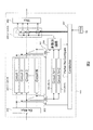
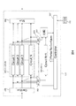
- the majority circuit 204 compares the three input signals and notifies the control unit 207 of the comparison result.
- the control unit 207 controls the selectors 202, 203, and 205-1 to 205-N.
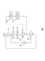
- the circuit configuration information of the FPGA is reset (written) and repaired by the above operation.
- the N signal processing circuits are sequentially inspected, if a problem occurs in the signal processing circuit 201-1 to 201-N circuit configuration information, the signal processing is performed until the inspection order comes around. Although there is a possibility that a problem occurs in the result, the time is shorter than the conventional technique described in Non-Patent Document 1, and higher reliability can be secured.
- control unit 207 when the control unit 207, the majority circuit 204, and the comparison circuit 208 are mounted in the FPGA in the first and second embodiments described above, the configuration information of these circuits may be destroyed. Therefore, it is also preferable to reset (write) the circuit configuration information of these circuits following the procedures 308, 309, and 310.
Landscapes
- Engineering & Computer Science (AREA)
- Physics & Mathematics (AREA)
- Mathematical Physics (AREA)
- General Engineering & Computer Science (AREA)
- Theoretical Computer Science (AREA)
- Computer Hardware Design (AREA)
- Computing Systems (AREA)
- Quality & Reliability (AREA)
- General Physics & Mathematics (AREA)
- Computer Security & Cryptography (AREA)
- Hardware Redundancy (AREA)
- Logic Circuits (AREA)
Abstract
La présente invention résout le problème consistant à éviter, dans un circuit de matrice prédiffusée programmable par l'utilisateur (FPGA) qui traite des signaux parallélisés, une réduction de fiabilité causée par la destruction d'informations de configuration de circuit, avec un petit accroissement de l'échelle du circuit. Le problème est résolu par un circuit configuré au moyen d'une FPGA caractérisée en ce qu'elle a un circuit de majorité qui prend une décision de majorité au moyen de la sortie d'au moins deux circuits et d'un signal sélectionné parmi la sortie d'une pluralité de circuits. La pluralité de circuits dispersent et effectuent le même processus, et les au moins deux circuits sélectionnent et entrent un signal d'entrée dans la pluralité de circuits, et effectuent le même processus. La FPGA est caractérisée en outre en ce que : quand toutes les entrées dans le circuit de majorité correspondent à un temps prédéfini, des signaux d'entrée entrés dans les au moins deux circuits qui ont été sélectionnés sont commutés à d'autres signaux d'entrée ; et quand une divergence dans les entrées du circuit de majorité est détectée, des informations de configuration de circuit pour les au moins deux circuits ou la pluralité de circuits qui produisent un signal de sortie sont réinitialisées.
Priority Applications (1)
| Application Number | Priority Date | Filing Date | Title |
|---|---|---|---|
| PCT/JP2013/057341 WO2014141455A1 (fr) | 2013-03-15 | 2013-03-15 | Circuit de matrice prédiffusée programmable par l'utilisateur |
Applications Claiming Priority (1)
| Application Number | Priority Date | Filing Date | Title |
|---|---|---|---|
| PCT/JP2013/057341 WO2014141455A1 (fr) | 2013-03-15 | 2013-03-15 | Circuit de matrice prédiffusée programmable par l'utilisateur |
Publications (1)
| Publication Number | Publication Date |
|---|---|
| WO2014141455A1 true WO2014141455A1 (fr) | 2014-09-18 |
Family
ID=51536150
Family Applications (1)
| Application Number | Title | Priority Date | Filing Date |
|---|---|---|---|
| PCT/JP2013/057341 Ceased WO2014141455A1 (fr) | 2013-03-15 | 2013-03-15 | Circuit de matrice prédiffusée programmable par l'utilisateur |
Country Status (1)
| Country | Link |
|---|---|
| WO (1) | WO2014141455A1 (fr) |
Cited By (2)
| Publication number | Priority date | Publication date | Assignee | Title |
|---|---|---|---|---|
| WO2016075800A1 (fr) * | 2014-11-14 | 2016-05-19 | 株式会社日立製作所 | Circuit programmable |
| JP6490316B1 (ja) * | 2018-02-28 | 2019-03-27 | 三菱電機株式会社 | 出力判定回路 |
Citations (2)
| Publication number | Priority date | Publication date | Assignee | Title |
|---|---|---|---|---|
| JP2012253657A (ja) * | 2011-06-06 | 2012-12-20 | Nec Engineering Ltd | 多数決回路を使用した半導体集積回路及び多数決方法 |
| WO2013027482A1 (fr) * | 2011-08-24 | 2013-02-28 | 株式会社日立製作所 | Dispositif programmable, procédé permettant de reconfigurer un dispositif programmable et dispositif électronique |
-
2013
- 2013-03-15 WO PCT/JP2013/057341 patent/WO2014141455A1/fr not_active Ceased
Patent Citations (2)
| Publication number | Priority date | Publication date | Assignee | Title |
|---|---|---|---|---|
| JP2012253657A (ja) * | 2011-06-06 | 2012-12-20 | Nec Engineering Ltd | 多数決回路を使用した半導体集積回路及び多数決方法 |
| WO2013027482A1 (fr) * | 2011-08-24 | 2013-02-28 | 株式会社日立製作所 | Dispositif programmable, procédé permettant de reconfigurer un dispositif programmable et dispositif électronique |
Cited By (2)
| Publication number | Priority date | Publication date | Assignee | Title |
|---|---|---|---|---|
| WO2016075800A1 (fr) * | 2014-11-14 | 2016-05-19 | 株式会社日立製作所 | Circuit programmable |
| JP6490316B1 (ja) * | 2018-02-28 | 2019-03-27 | 三菱電機株式会社 | 出力判定回路 |
Similar Documents
| Publication | Publication Date | Title |
|---|---|---|
| EP2492917B1 (fr) | Circuit de détection et de correction d'erreurs | |
| KR101519491B1 (ko) | 누적 테스트를 위한 반도체 메모리 장치 및 이를 포함하는 시스템 | |
| US9437323B2 (en) | Shift register circuit for preventing malfunction due to clock skew and memory device including the same | |
| JPWO2008023577A1 (ja) | 故障予測回路と方法及び半導体集積回路 | |
| US9583216B2 (en) | MBIST device for use with ECC-protected memories | |
| US10665316B2 (en) | Memory device | |
| US9575862B1 (en) | Integrated circuits with error handling capabilities | |
| US20130305000A1 (en) | Signal processing circuit | |
| KR20090012499A (ko) | 실장테스트회로를 구비하는 반도체 메모리 장치 및실장테스트방법 | |
| JP2020048022A (ja) | 半導体集積回路及び再構成半導体システム | |
| US8522091B1 (en) | Prioritized detection of memory corruption | |
| CN112988476A (zh) | 包含安全装置的三重寄存器 | |
| US10318376B2 (en) | Integrated circuit and programmable device | |
| WO2014141455A1 (fr) | Circuit de matrice prédiffusée programmable par l'utilisateur | |
| KR102076770B1 (ko) | 반도체 장치 | |
| US11715544B2 (en) | System and method for low power memory test | |
| US8516336B2 (en) | Latch arrangement for an electronic digital system, method, data processing program, and computer program product for implementing a latch arrangement | |
| US10018675B1 (en) | Testing an integrated circuit in user mode using partial reconfiguration | |
| JPWO2015068207A1 (ja) | プログラマブルデバイス | |
| CN110827878B (zh) | 存储器装置 | |
| US8458545B2 (en) | Method and apparatus for testing of a memory with redundancy elements | |
| JP5612249B2 (ja) | 半導体記憶装置 | |
| JP6194679B2 (ja) | データ補正回路及びデータ補正方法 | |
| JP2015201813A (ja) | プログラマブルゲートアレイ | |
| US9208040B2 (en) | Repair control logic for safe memories having redundant elements |
Legal Events
| Date | Code | Title | Description |
|---|---|---|---|
| 121 | Ep: the epo has been informed by wipo that ep was designated in this application |
Ref document number: 13877969 Country of ref document: EP Kind code of ref document: A1 |
|
| NENP | Non-entry into the national phase |
Ref country code: DE |
|
| 122 | Ep: pct application non-entry in european phase |
Ref document number: 13877969 Country of ref document: EP Kind code of ref document: A1 |
|
| NENP | Non-entry into the national phase |
Ref country code: JP |