WO2014141668A1 - Dispositif magnétique - Google Patents
Dispositif magnétique Download PDFInfo
- Publication number
- WO2014141668A1 WO2014141668A1 PCT/JP2014/001319 JP2014001319W WO2014141668A1 WO 2014141668 A1 WO2014141668 A1 WO 2014141668A1 JP 2014001319 W JP2014001319 W JP 2014001319W WO 2014141668 A1 WO2014141668 A1 WO 2014141668A1
- Authority
- WO
- WIPO (PCT)
- Prior art keywords
- substrate
- patterns
- surface layer
- heat
- heat radiation
- Prior art date
- Legal status (The legal status is an assumption and is not a legal conclusion. Google has not performed a legal analysis and makes no representation as to the accuracy of the status listed.)
- Ceased
Links
Images


Classifications
-
- H—ELECTRICITY
- H01—ELECTRIC ELEMENTS
- H01F—MAGNETS; INDUCTANCES; TRANSFORMERS; SELECTION OF MATERIALS FOR THEIR MAGNETIC PROPERTIES
- H01F37/00—Fixed inductances not covered by group H01F17/00
-
- H—ELECTRICITY
- H01—ELECTRIC ELEMENTS
- H01F—MAGNETS; INDUCTANCES; TRANSFORMERS; SELECTION OF MATERIALS FOR THEIR MAGNETIC PROPERTIES
- H01F27/00—Details of transformers or inductances, in general
- H01F27/08—Cooling; Ventilating
- H01F27/22—Cooling by heat conduction through solid or powdered fillings
-
- H—ELECTRICITY
- H01—ELECTRIC ELEMENTS
- H01F—MAGNETS; INDUCTANCES; TRANSFORMERS; SELECTION OF MATERIALS FOR THEIR MAGNETIC PROPERTIES
- H01F27/00—Details of transformers or inductances, in general
- H01F27/28—Coils; Windings; Conductive connections
- H01F27/2804—Printed windings
-
- H—ELECTRICITY
- H05—ELECTRIC TECHNIQUES NOT OTHERWISE PROVIDED FOR
- H05K—PRINTED CIRCUITS; CASINGS OR CONSTRUCTIONAL DETAILS OF ELECTRIC APPARATUS; MANUFACTURE OF ASSEMBLAGES OF ELECTRICAL COMPONENTS
- H05K1/00—Printed circuits
- H05K1/02—Details
- H05K1/0201—Thermal arrangements, e.g. for cooling, heating or preventing overheating
- H05K1/0203—Cooling of mounted components
- H05K1/0204—Cooling of mounted components using means for thermal conduction connection in the thickness direction of the substrate
-
- H—ELECTRICITY
- H01—ELECTRIC ELEMENTS
- H01F—MAGNETS; INDUCTANCES; TRANSFORMERS; SELECTION OF MATERIALS FOR THEIR MAGNETIC PROPERTIES
- H01F27/00—Details of transformers or inductances, in general
- H01F27/28—Coils; Windings; Conductive connections
- H01F27/2804—Printed windings
- H01F2027/2819—Planar transformers with printed windings, e.g. surrounded by two cores and to be mounted on printed circuit
-
- H—ELECTRICITY
- H05—ELECTRIC TECHNIQUES NOT OTHERWISE PROVIDED FOR
- H05K—PRINTED CIRCUITS; CASINGS OR CONSTRUCTIONAL DETAILS OF ELECTRIC APPARATUS; MANUFACTURE OF ASSEMBLAGES OF ELECTRICAL COMPONENTS
- H05K1/00—Printed circuits
- H05K1/16—Printed circuits incorporating printed electric components, e.g. printed resistors, capacitors or inductors
- H05K1/165—Printed circuits incorporating printed electric components, e.g. printed resistors, capacitors or inductors incorporating printed inductors
-
- H—ELECTRICITY
- H05—ELECTRIC TECHNIQUES NOT OTHERWISE PROVIDED FOR
- H05K—PRINTED CIRCUITS; CASINGS OR CONSTRUCTIONAL DETAILS OF ELECTRIC APPARATUS; MANUFACTURE OF ASSEMBLAGES OF ELECTRICAL COMPONENTS
- H05K2201/00—Indexing scheme relating to printed circuits covered by H05K1/00
- H05K2201/08—Magnetic details
- H05K2201/083—Magnetic materials
- H05K2201/086—Magnetic materials for inductive purposes, e.g. printed inductor with ferrite core
-
- H—ELECTRICITY
- H05—ELECTRIC TECHNIQUES NOT OTHERWISE PROVIDED FOR
- H05K—PRINTED CIRCUITS; CASINGS OR CONSTRUCTIONAL DETAILS OF ELECTRIC APPARATUS; MANUFACTURE OF ASSEMBLAGES OF ELECTRICAL COMPONENTS
- H05K2201/00—Indexing scheme relating to printed circuits covered by H05K1/00
- H05K2201/10—Details of components or other objects attached to or integrated in a printed circuit board
- H05K2201/10227—Other objects, e.g. metallic pieces
- H05K2201/10409—Screws
-
- H—ELECTRICITY
- H05—ELECTRIC TECHNIQUES NOT OTHERWISE PROVIDED FOR
- H05K—PRINTED CIRCUITS; CASINGS OR CONSTRUCTIONAL DETAILS OF ELECTRIC APPARATUS; MANUFACTURE OF ASSEMBLAGES OF ELECTRICAL COMPONENTS
- H05K3/00—Apparatus or processes for manufacturing printed circuits
- H05K3/0058—Laminating printed circuit boards onto other substrates, e.g. metallic substrates
- H05K3/0061—Laminating printed circuit boards onto other substrates, e.g. metallic substrates onto a metallic substrate, e.g. a heat sink
Definitions
- the present invention relates to a magnetic device such as a choke coil or a transformer including a core made of a magnetic material and a substrate on which a coil pattern is formed.
- a switching power supply device such as a DC-DC converter (DC-DC converter) that switches a high-voltage direct current to a alternating current after switching to a low-voltage direct current.
- the switching power supply device uses a magnetic device such as a choke coil or a transformer.
- Patent Documents 1 to 6 disclose a magnetic device including a coil pattern in which a coil winding is formed on a substrate.
- a core made of a magnetic material penetrates the substrate.
- the substrate is made of an insulator and has a plurality of layers.
- a coil pattern is formed on each layer so as to be wound around the core.
- Coil patterns of different layers are connected by through holes or the like.
- the coil pattern and the through hole are made of a conductor such as copper.
- a substrate is composed of a pair of insulating layers and a magnetic layer sandwiched between the insulating layers.
- a coil pattern made of a conductor is formed on the magnetic layer. The coil pattern is wound a plurality of times in the plate surface direction and the thickness direction of the substrate.
- Patent Document 1 When a current flows through the coil pattern, heat is generated from the coil pattern and the substrate temperature rises.
- the coil pattern is spread over almost the entire area of each layer of the substrate.
- patent document 3 the width
- Patent Document 6 a heat-dissipating conductor layer is provided on the inner side of the coil pattern, the heat-transmitting penetrating conductor penetrating the magnetic layer and the lower insulating layer, and connected to the heat-transmitting penetrating conductor on the lower surface of the substrate. Is provided.
- JP 2008-205350 A Japanese Unexamined Patent Publication No. 7-38262 JP-A-7-86755 Reissue WO2010 / 026690 JP-A-8-69935 JP 2008-177516 A
- An object of the present invention is to provide a magnetic device that can easily dissipate heat from a substrate provided with a coil pattern without increasing the size.
- a magnetic device includes a core made of a magnetic material, a substrate made of an insulator, through which the core penetrates, and a conductor provided on the substrate including a coil pattern wound around the core. .
- a radiator is provided on the back side of the substrate, and the area of the conductor provided on the back layer of the substrate is larger than the area of the conductor provided on the surface layer of the substrate.
- the heat of the substrate on which the coil pattern is provided can be easily transferred from the conductor having a large area provided on the back surface layer to the radiator, so that the substrate can be easily dissipated.
- the width of the coil pattern does not have to be increased over the entire length of the coil pattern so that the amount of generated heat is reduced, and the magnetic device can be prevented from being enlarged.
- the conductor provided on the front surface layer and the back surface layer of the substrate may include a coil pattern and a heat radiation pattern formed integrally or separately from the coil pattern. Good.
- the substrate and the radiator may be fixed with screws in a region where no conductor exists on the surface layer of the substrate.
- an insulating sheet having heat conductivity may be sandwiched between the substrate and the radiator.
- the present invention it is possible to provide a magnetic device that can easily dissipate heat from a substrate provided with a coil pattern without increasing its size.
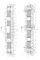
- FIG. 1 is an exploded perspective view of a magnetic device according to a first embodiment of the present invention. It is a top view of each layer of the board
- FIG. 1 is a configuration diagram of the switching power supply device 100.
- the switching power supply device 100 is a DC-DC converter for an electric vehicle (or a hybrid car), which switches a high voltage direct current to an alternating current and then converts it to a low voltage direct current. This will be described in detail below.
- the high voltage battery 50 is connected to the input terminals T1 and T2 of the switching power supply apparatus 100.
- the voltage of the high voltage battery 50 is, for example, DC 220V to DC 400V.
- the DC voltage Vi of the high-voltage battery 50 input to the input terminals T1 and T2 is applied to the switching circuit 52 after noise is removed by the filter circuit 51.
- the switching circuit 52 is formed of a known circuit having, for example, an FET (Field Effect Transistor).
- the FET is turned on / off based on a PWM (Pulse Width Modulation: pulse width modulation) signal from the PWM drive unit 58 to perform a switching operation on the DC voltage.
- PWM Pulse Width Modulation: pulse width modulation
- the pulse voltage is given to the rectifier circuit 54 via the transformer 53.
- the rectifier circuit 54 rectifies the pulse voltage by a pair of diodes D1 and D2.
- the voltage rectified by the rectifier circuit 54 is input to the smoothing circuit 55.
- the smoothing circuit 55 smoothes the rectified voltage by the filtering action of the choke coil L and the capacitor C, and outputs the smoothed voltage to the output terminals T3 and T4 as a low DC voltage.
- the low voltage battery 60 connected to the output terminals T3 and T4 is charged to, for example, DC12V.
- the DC voltage of the low-voltage battery 60 is supplied to various on-vehicle electrical components (not shown).
- the output voltage Vo of the smoothing circuit 55 is detected by the output voltage detection circuit 59 and then output to the PWM drive unit 58.
- the PWM drive unit 58 calculates the duty ratio of the PWM signal based on the output voltage Vo, generates a PWM signal corresponding to the duty ratio, and outputs the PWM signal to the gate of the FET of the switching circuit 52. As a result, feedback control is performed to keep the output voltage constant.
- the control unit 57 controls the operation of the PWM drive unit 58.
- a power source 56 is connected to the output side of the filter circuit 51.
- the power supply 56 steps down the voltage of the high voltage battery 50 and supplies a power supply voltage (for example, DC 12 V) to the control unit 57.
- magnetic devices 1 and 1 'described later are used as the choke coil L of the smoothing circuit 55.
- a large current of, for example, DC 150A flows through the choke coil L.
- terminals 6i and 6o for power input / output are provided.
- FIG. 2 is an exploded perspective view of the magnetic device 1.
- FIG. 3 is a plan view of each layer of the substrate 3 of the magnetic device 1.
- 4A and 4B are cross-sectional views of the magnetic device 1, wherein FIG. 4A shows the XX cross section of FIG. 3, and FIG. 4B shows the YY cross section of FIG.
- the cores 2a and 2b are composed of two pairs of an E-shaped upper core 2a and an I-shaped lower core 2b.
- the cores 2a and 2b are made of a magnetic material such as ferrite or amorphous metal.
- the upper core 2a has three convex portions 2m, 2L, and 2r so as to protrude downward.
- the left and right protrusions 2L and 2r have a larger amount of protrusion than the center protrusion 2m.
- the lower ends of the left and right convex portions 2L, 2r of the upper core 2a are brought into close contact with the upper surface of the lower core 2b, and the cores 2a, 2b are combined.
- a gap of a predetermined size is provided on the upper surface of the convex portion 2m of the upper core 2a and the upper surface of the lower core 2b in order to improve the DC superimposition characteristics.
- the cores 2a and 2b are fixed by fixing means such as screws and metal fittings (not shown).
- the lower core 2 b is fitted into a recess 10 k (FIG. 2) provided on the upper side of the heat sink 10.
- a fin 10 f is provided on the lower side of the heat sink 10.
- the heat sink 10 is made of metal and is an example of the “heat radiator” of the present invention.
- the substrate 3 is composed of a thick copper foil substrate in which a pattern is formed of a thick copper foil (conductor) on each layer of a thin plate-like base material made of an insulator.
- other electronic components and circuits are not provided on the substrate 3, but when the magnetic device 1 is actually used in the switching power supply device 100 of FIG. 1, the magnetic device 1 and the switching power supply device are provided on the same substrate. 100 other electronic components and circuits are provided (the same applies to a magnetic device 1 ′ described later).
- a surface layer L1 as shown in FIG. 3A is provided on the surface of the substrate 3 (the upper surface in FIGS. 2 and 4).
- a back surface layer L3 as shown in FIG. 3C is provided on the back surface of the substrate 3 (the bottom surface in FIGS. 2 and 4).
- an intermediate layer L2 as shown in FIG. 3B is provided between the front surface layer L1 and the back surface layer L3. That is, the substrate 3 has three layers L1, L2, and L3 that can form a circuit.
- the substrate 3 is provided with a plurality of through holes 3m, 3L, 3r, and 3a. Among them, the convex portions 2m, 2L, and 2r of the core 2a are inserted into the large-diameter through holes 3m, 3L, and 3r, respectively, as shown in FIGS. That is, the convex portions 2m, 2L, and 2r of the core 2a penetrate the substrate 3.
- Each screw 11 is inserted into the plurality of small diameter through holes 3a as shown in FIG.
- the back surface (back surface layer L3) of the substrate 3 is opposed to the upper surface of the heat sink 10 (the surface opposite to the fin 10f). Then, the screws 11 are passed through the through holes 3 a from the surface (surface layer L 1) side of the substrate 3 and screwed into the screw holes 10 a of the heat sink 10. Thereby, as shown in FIG. 4, the heat sink 10 is fixed to the back surface side of the board
- An insulating sheet 12 having heat conductivity is sandwiched between the substrate 3 and the heat sink 10. Since the insulating sheet 12 has flexibility, it is in close contact with the substrate 3 and the heat sink 10 without a gap.
- the substrate 3 is provided with conductors such as through holes 8a, 8d, 9a to 9d, pads 8b and 8c, terminals 6i and 6o, patterns 4a to 4f, 5a to 5e, and pins 7a to 7f. It has been.
- the through holes 8a, 8d, 9a to 9d connect the patterns 4a to 4f and 5c to 5e in the different layers L1, L2, and L3.
- the plurality of through holes 8a connect the patterns 4a and 4b of the upper layer L1 to the other layers L2 and L3.
- Each through hole 8d connects the upper layer L1 and the other layers L2, L3, connects the patterns 4a, 4b of the upper layer L1 and the pattern 5e of the lower layer L3, and connects the patterns 4c, 4d of the intermediate layer L2 and the lower layer L3.
- the patterns 5c and 5d are connected.
- the through holes 9a and 9d connect the patterns 4a and 4b of the upper layer L1 and the patterns 4c and 4d of the intermediate layer L2.
- the through holes 9b and 9c connect the patterns 4c and 4d of the intermediate layer L2 and the pattern 4e of the lower layer L3.
- one through hole 8a has a power input terminal 6i embedded therein.
- a power output terminal 6o is embedded in the other through hole 8a.
- Terminals 6i and 6o are made of copper pins.
- a pad 8b made of copper foil is provided around the terminals 6i and 6o of the front surface layer L1 and the back surface layer L3. Copper plating is applied to the surfaces of the terminals 6i and 6o and the pad 8b. The lower ends of the terminals 6i and 6o are in contact with the insulating sheet 12 (not shown).
- the heat dissipation pins 7a to 7f are embedded in the plurality of large-diameter through holes 8d.
- the radiating pins 7a to 7f are made of copper pins.
- a pad 8c made of copper foil is provided around the heat radiation pins 7a to 7f of the front surface layer L1 and the back surface layer L3. Copper plating is applied to the surfaces of the heat radiation pins 7a to 7f and the pad 8c.
- the lower ends of the heat radiation pins 7a to 7f are in contact with the insulating sheet 12 (see FIG. 4A).
- each layer L1, L2, L3 of the substrate 3 coil patterns 4a to 4e and heat radiation patterns 5a to 5e are provided.
- Each pattern 4a to 4e, 5a to 5e is made of copper foil.
- the surfaces of the patterns 4a to 4e and 5a to 5e of the surface layer L1 are subjected to insulation processing.
- the width, thickness, and cross-sectional area of the coil patterns 4a to 4e can suppress the amount of heat generated from the coil patterns 4a to 4e to some extent even when a predetermined large current (for example, DC150A) flows, and the coil patterns 4a to 4e. It is set to be able to dissipate heat from the surface.
- a predetermined large current for example, DC150A
- the coil pattern 4a is wound once in the four directions around the convex portion 2L.
- the coil pattern 4b is wound once in four directions around the convex portion 2r.
- the coil pattern 4c is wound once in the four directions around the convex portion 2L.
- the coil pattern 4d is wound once in the four directions around the convex portion 2r.
- the coil pattern 4e is wound once in the four directions around the convex portion 2L, and then wound once in the three directions around the convex portion 2m. Further, it is wound once in four directions around the convex portion 2r.
- One end of the coil pattern 4a and one end of the coil pattern 4c are connected by a through hole 9a.
- the other end of the coil pattern 4c and one end of the coil pattern 4e are connected by a through hole 9c.
- the other end of the coil pattern 4e and one end of the coil pattern 4d are connected by a through hole 9b.
- the other end of the coil pattern 4d and one end of the coil pattern 4b are connected by a through hole 9d.
- Small patterns 4f are provided around the through holes 9b and 9c of the surface layer L1 and around the through holes 9a and 9d of the back layer L3 in order to facilitate the formation of the through holes 9a to 9d.
- the respective through holes 9a to 9d and the small pattern 4f are connected.
- the small pattern 4f is made of copper foil.
- the surface of the small pattern 4f of the surface layer L1 is subjected to insulation processing. Copper plating is applied to the surface of each through hole 9a to 9d.
- the inside of each through hole 9a-9d may be filled with copper or the like.
- the other end of the coil pattern 4a is connected to a terminal 6i through a pad 8b.
- the other end of the coil pattern 4b is connected to the terminal 6o through a pad 8b.
- the coil patterns 4a to 4e of the substrate 3 are the surface layer L1, and after the first turn is wound around the convex portion 2L from the starting terminal 6i, the intermediate layer L2 is passed through the through hole 9a. Connected to. Next, in the intermediate layer L2, the second time is wound around the convex portion 2L, and then connected to the back surface layer L3 via the through hole 9c.
- the coil pattern is the back surface layer L3, the third time is wound around the convex portion 2L, the fourth time is wound around the convex portion 2r via the periphery of the convex portion 2m, and then the through hole is formed. It is connected to the intermediate layer L2 via 9b.
- the coil pattern is the intermediate layer L2, and after the fifth round is wound around the convex portion 2r, it is connected to the surface layer L1 via the through hole 9d.
- the coil pattern is the surface layer L1, and after the sixth time is wound around the convex portion 2r, the coil pattern is connected to the terminal 6o that is the end point.
- the current flowing through the magnetic device 1 is also the terminal 6i, the coil pattern 4a, the through hole 9a, the coil pattern 4c, the through hole 9c, the coil pattern 4e, the through hole 9b, the coil pattern 4d, the through hole 9d, and the coil pattern. 4b and terminal 6o in this order.
- the heat radiation patterns 5a to 5e are formed separately from the patterns 4a to 4e and 4f in the empty areas around the coil patterns 4a to 4e and the small patterns 4f of the layers L1 to L3.
- the pad 8b, the terminals 6i and 6o, the through hole 3a, and the screw 11 are insulated from the heat radiation patterns 5a to 5e.
- the shortest insulation distance S1 between the through-hole 3a in the surface layer L1 and the heat radiation pattern 5a is larger than the shortest insulation distance S2 between the through-hole 3a in the intermediate layer L2 and the back layer L3 and the heat radiation patterns 5b to 5e. It is getting bigger.
- the head portion 11a having a diameter larger than the shaft portion 11b of the screw 11 is disposed on the surface side of the substrate 3, so that the head portion 11a and the heat radiation pattern 5a are insulated. That is, the substrate 3 and the heat sink 10 are fixed by the screws 11 in the regions R1 and R2 where no conductor exists in each of the layers L1 to L3 of the substrate 3.
- the heat radiation pin 7a and the surrounding pad 8c are connected to the coil pattern 4a. Further, the heat radiation pin 7b and the surrounding pad 8c are connected to the coil pattern 4b. The heat radiation pins 7c to 7f and the surrounding pad 8c are insulated from the heat radiation pattern 5a. Further, the coil patterns 4a, 4b and the small pattern 4f are insulated from the heat radiation pattern 5a.
- heat radiation pins 7c and 7e are connected to the coil pattern 4c.
- heat radiation pins 7d and 7f are connected to the coil pattern 4d.
- the heat radiation pin 7a is insulated from the heat radiation pattern 5b.
- the coil patterns 4c and 4d are insulated from the heat radiation pattern 5b.
- the heat radiation pins 7a to 7f and the surrounding pads 8c are connected to the heat radiation patterns 5c to 5e. Further, the coil pattern 4e and the small pattern 4f are insulated from the heat radiation patterns 5c to 5e.
- the coil patterns 4a and 4b on the front surface layer L1 and the left and right heat radiation patterns 5e on the back surface layer L3 are connected by the heat radiation pins 7a and 7b, respectively. Further, the coil patterns 4c and 4d of the intermediate layer L2 and the left and right heat radiation patterns 5c and 5d of the back surface layer L3 are connected by the heat radiation pins 7c to 7f, respectively.
- the surface areas of the through holes 8a, 8d, 9a to 9d, which are conductors, the pads 8b and 8c, the terminals 6i and 6o, the small pattern 4f, and the pins 7a to 7f are the same. Further, the total surface area of the coil patterns 4a and 4b of the surface layer L1 is larger than the surface area of the coil pattern 4e of the back surface layer L3.
- the total surface area of the heat radiation patterns 5c to 5e of the back surface layer L3 is larger than the surface area of the heat radiation pattern 5a of the front surface layer L1. This is apparent when attention is paid to the regions R1 and R2 around the screw 11.
- the difference in surface area between the heat radiation patterns 5a, 5c to 5e of the surface layer L1 and the back surface layer L3 is larger than the difference in surface area between the coil patterns 4a, 4b, 4e.
- the area of the conductor provided in the surface layer L1 (the total of the through holes 8a, 8d, 9a to 9d, the pads 8b and 8c, the terminals 6i and 6o, the patterns 4a, 4b, 4f, and 5a, and the pins 7a to 7f)
- Area of the conductor provided in the back surface layer L3 (through holes 8a, 8d, 9a to 9d, pads 8b and 8c, terminals 6i and 6o, patterns 4e, 4f, 5c to 5e, and pins 7a to 7f). The total surface area) is wider.
- the surface areas of the through holes 8a, 8d, 9a to 9d, the terminals 6i and 6o, and the pins 7a to 7f, which are conductors, are the same. Further, there is almost no difference in the surface areas of the patterns 4a, 4b, 4c, 4d, and 4f of the surface layer L1 and the intermediate layer L2. Further, the pads 8b and 8c in the surface layer L1 are not in the intermediate layer L2.
- the surface area of the heat radiation pattern 5b of the intermediate layer L2 is larger than the surface area of the heat radiation pattern 5a of the surface layer L1. This is apparent when attention is paid to the regions R1 and R2 around the screw 11.
- the difference in surface area between the heat radiation patterns 5a and 5b of the surface layer L1 and the intermediate layer L2 is larger than the surface area of the pads 8b and 8c.
- the area of the conductor provided in the surface layer L1 (the total of the through holes 8a, 8d, 9a to 9d, the pads 8b and 8c, the terminals 6i and 6o, the patterns 4a, 4b, 4f, and 5a, and the pins 7a to 7f)
- the surface area of the conductor provided in the intermediate layer L2 (the total surface area of the through holes 8a, 8d, 9a to 9d, the terminals 6i and 6o, the patterns 4c, 4d, and 5b, and the pins 7a to 7f) is wider than the surface area). It has become.
- the coil patterns 4a to 4e serve as heat generation sources, and the temperature of the substrate 3 rises.
- the heat of the substrate 3 is diffused to a conductor such as the heat radiation pattern 5a and is radiated on the surface of the conductor.
- the heat of the substrate 3 is radiated by the heat sink 10 through the insulating sheet 12 through conductors that penetrate the substrate 3 such as the heat radiation pins 7a and 7f and the through holes 8d, 8a, and 9a to 9d.
- the heat generation of the coil patterns 4a and 4b of the surface layer L1 is transmitted through the heat dissipation pins 7a and 7b, the terminals 6i and 6o, the through holes 8d, 8a, 9a and 9d, and the heat dissipation pattern 5e of the back surface layer L3, thereby Heat is radiated by the heat sink 10 through 12.
- the through holes 9a to 9d also function as thermal vias.
- the heat of the substrate 3 is diffused to a conductor such as the heat radiation pattern 5b.
- the heat of the substrate 3 is radiated by the heat sink 10 through the insulating sheet 12 through conductors that penetrate the substrate 3 such as the heat radiation pins 7c to 7f and the through holes 8d and 9a to 9d.
- the heat generation of the coil patterns 4c and 4d of the intermediate layer L2 is transmitted through the heat radiation pins 7c, 7d, 7e and 7f, the through holes 8d and 9a to 9d, and the heat radiation patterns 5c and 5d of the back surface layer L3, to the insulating sheet 12.
- the heat sink 10 dissipates heat.
- the heat of the substrate 3 is diffused to conductors such as the heat radiation patterns 5c to 5e and the heat radiation pins 7a to 7f.
- the heat diffused in these conductors is radiated by the heat sink 10 through the insulating sheet 12.
- the heat generated by the coil pattern 4e is radiated by the heat sink 10 through the insulating sheet 12 from the surface of the coil pattern 4e.
- the heat of the substrate 3 provided with the coil patterns 4a to 4e is easily transferred to the heat sink 10 from the conductor having a large area provided on the back surface layer L3. can do. Thereby, heat generation of the coil patterns 4a to 4e is allowed. As a result, the width of the coil patterns 4a to 4e does not have to be increased over the entire length of the coil patterns 4a to 4e so that the heat generation amount is reduced, and the magnetic device 1 can be prevented from being enlarged.
- the heat of the substrate 3 can be radiated from the front surface side and the back surface side of the substrate 3.
- heat can be efficiently transferred to the heat sink 10 from the surface of the coil pattern 4e and the heat radiation patterns 5c to 5e to be radiated.
- heat can be radiated from the surfaces of the coil patterns 4a and 4b and the heat radiation pattern 5a.
- the screws 11 and the conductors of the substrate 3 can be securely connected even if the screws 11 are not insulated. Can be insulated.
- the head 11a of the screw 11 on the surface layer L1 side of the substrate 3 and providing a region R1 in which no conductor exists around the head 11a, the back surface layer L3 from the area of the conductor of the surface layer L1.
- the area of the conductor can be easily increased.
- the substrate 3 and the heat sink 10 can be insulated without applying insulation processing to the back surface layer L3 of the substrate 3, The heat of the substrate 3 can be transferred to the heat sink 10.
- the present invention is not limited to this.
- a heat radiation pattern integrated with the coil pattern may be provided.
- FIG. 5 is a plan view of each layer of the substrate 3 ′ of the magnetic device 1 ′ according to the second embodiment.
- FIG. 6 is a cross-sectional view of the magnetic device 1 ′ and shows a ZZ cross-section of FIG. 5.
- the cores 2 a ′ and 2 b ′ made of a magnetic material are composed of a pair of an upper core 2 a ′ having an E shape and a lower core 2 b ′ having an I shape.
- the lower ends of the left and right convex portions 2L ′ and 2r ′ are brought into close contact with the upper surface of the lower core 2b ′, and the core 2a ′. 2b 'are combined.
- a gap having a predetermined size is provided on the upper surface of the protrusion 2m 'of the upper core 2a' and the lower core 2b '.
- the cores 2a 'and 2b' are fixed by fixing means such as screws or metal fittings (not shown).
- the lower core 2 b ′ is fitted into a recess 10 k provided on the upper side of the heat sink 10.
- the substrate 3 ' is composed of a thick copper foil substrate having a front surface layer L1', an intermediate layer L2 ', and a back surface layer L3'.
- the central protrusion 2m 'of the cores 2a' and 2b ' passes through the through hole 3m' of the substrate 3 '.
- the left and right notches 3k have left and right protrusions 2L 'and 2r' of the cores 2a 'and 2b'.
- the back surface of the substrate 3 ′ is opposed to the upper surface of the heat sink 10, and as shown in FIG. 6, the screw 11 is passed through the through hole 3 a from the surface side of the substrate 3 ′ and screwed into the screw hole 10 a of the heat sink 10. Thereby, the heat sink 10 is fixed to the back surface side of the substrate 3 ′ in the proximity state.
- An insulating sheet 12 is sandwiched between the substrate 3 ′ and the heat sink 10.
- the substrate 3 ′ has through holes 8a, 8d, 9a ′, 9b ′, pads 8b, 8c, terminals 6i, 6o, patterns 4a ′, 4b ′, 4c ′, 4f ′, 5t 0.
- Conductors such as ⁇ 5t 6 , 5s 0 ⁇ 5s 9 , and pins 7g 0 ⁇ 7g 3 are provided.
- Terminals 6i and 6o are respectively embedded in the through holes 8a.
- Pads 8b are provided around the terminals 6i and 6o of the surface layer L1 ′ and the back surface layer L3 ′.
- Radiation pins 7g 0 to 7g 3 are embedded in the through holes 8d, respectively.
- the heat radiation pins 7g 0 to 7g 3 are made of copper pins, and the surfaces thereof are plated with copper.
- a pad 8c is provided around the heat radiation pins 7g 0 to 7g 3 of the surface layer L1 ′ and the back surface layer L3 ′. The lower ends of the radiating pins 7g 0 to 7g 3 are in contact with the insulating sheet 12.
- each layer L1 ′ to L3 ′ coil patterns 4a ′ to 4c ′ and heat radiation patterns 5t 0 to 5t 6 and 5s 0 to 5s 9 are provided.
- Each of the patterns 4a ′ to 4c ′, 5t 0 to 5t 6 , and 5s 0 to 5s 9 is made of a copper foil.
- the surface of each pattern 4a ′ to 4c ′, 5t 0 to 5t 6 , 5s 0 to 5s 9 of the surface layer L1 ′ is subjected to insulation processing.
- the width, thickness, and cross-sectional area of the coil patterns 4a ′ to 4c ′ can suppress the amount of heat generated from the coil patterns 4a ′ to 4c ′ to a certain extent even when a predetermined large current (for example, DC 150A) flows.
- the heat radiation is set from the surface of the patterns 4a ′ to 4c ′.
- the coil patterns 4a 'to 4c' are wound twice around the central convex portion 2m '.
- One end of the coil pattern 4a 'and one end of the coil pattern 4b' are connected by a through hole 9a '.
- the other end of the coil pattern 4b 'and one end of the coil pattern 4c' are connected by a through hole 9b '.
- the other end of the coil pattern 4a ' is connected to the terminal 6o via the pad 8b on the surface layer L1'.
- the other end of the coil pattern 4c ' is connected to the terminal 6i through the pad 8b on the back surface layer L3'.
- Small patterns 4 f ′ made of copper foil are provided around the through hole 9 b ′ of the front surface layer L ⁇ b> 1 ′ and around the through hole 9 a ′ of the back surface layer L ⁇ b> 3 ′.
- the respective through holes 9a 'and 9b' are connected to the small pattern 4f '.
- the surface of the small pattern 4f 'of the surface layer L1' is subjected to insulation processing. Copper plating is applied to the surface of each through hole 9a ', 9b'.
- the coil patterns 4a ′ to 4c ′ of the substrate 3 ′ are formed on the back surface layer L3 ′ after the first and second windings around the convex portion 2m ′ from the starting terminal 6i, and then through holes 9b. It is connected to the intermediate layer L2 'via'.
- the coil pattern is the intermediate layer L2 ', and after the third and fourth turns are wound around the convex portion 2m', the coil pattern is connected to the surface layer L1 'through the through hole 9a'.
- the coil pattern is connected to the terminal 6o which is the end point after the fifth and sixth turns are wound around the convex portion 2m 'on the surface layer L1'.
- the current flowing through the magnetic device 1 ' also flows along the above-described normal path.
- the heat radiation patterns 5t 0 to 5t 6 and 5s 0 to 5s 9 are formed in empty areas around the coil patterns 4a ′ to 4c ′ and the small patterns 4f ′ of the layers L1 ′ to L3 ′.
- the heat radiation patterns 5t 0 to 5t 6 are formed integrally with the coil patterns 4a ′ to 4c ′ by extending the coil patterns 4a ′ to 4c ′.
- the heat radiation patterns 5s 0 to 5s 9 are formed separately from the coil patterns 4a ′ to 4c ′, the small pattern 4f ′, and the heat radiation patterns 5t 0 to 5t 6 .
- the heat radiation patterns 5s 0 to 5s 2 are insulated from each other, and are also insulated from the heat radiation patterns 5t 0 to 5t 2 and the coil pattern 4a ′.
- the radiating pins 7g 0 and 7g 1 and the surrounding pads 8c are provided in the radiating patterns 5t 0 and 5t 1 respectively, and are connected to the radiating patterns 5t 0 to 5t 2 and the coil pattern 4a ′.
- the surrounding terminal 6o pad 8b is provided on the heat radiation pattern 5t 2, heat radiation patterns 5t 0 ⁇ 5t 2 and coil patterns 4a' surface layer L1 is connected to the heat radiation pattern 5s 0 ⁇ 5s 2 and are insulated.
- the terminal 6i and the surrounding pad 8b are insulated from the coil pattern 4a ′ and the heat radiation patterns 5t 0 to 5t 2 .
- the radiating pins 7g 2 and 7g 3 and the surrounding pad 8c are provided in the radiating patterns 5s 1 and 5s 2 respectively, and are connected to the radiating patterns 5s 1 and 5s 2, and the radiating patterns 5s 0 , 5t 0 to 5t. 2 and the coil pattern 4a ′.
- the heat radiation patterns 5s 3 , 5s 4 are insulated from each other, and further, the heat radiation patterns 5t 3 , 5t 4 and the coil pattern 4b ′ are also insulated.
- the heat radiation pins 7g 2 and 7g 3 and the surrounding through holes 8d are provided in the heat radiation patterns 5t 3 and 5t 4 , respectively, and the heat radiation patterns 5t 3 and 5t 4 and the coil pattern 4b. 'It is connected to the.
- Radiation fins 7 g 0, 7 g 1 and through holes 8d in the surroundings is provided respectively on the heat radiation pattern 5s 3, 5s 4, is connected to the heat radiation pattern 5s 3, 5s 4, the heat radiation pattern 5t 3, 5t 4 Ya It is insulated from the coil pattern 4b ′.
- the heat radiation patterns 5s 5 to 5s 9 are insulated from each other, and are also insulated from the heat radiation patterns 5t 5 , 5t 6 and the coil pattern 4c ′.
- the radiating pins 7g 0 to 7g 3 and the surrounding pads 8c are provided in the radiating patterns 5s 5 to 5s 8 , respectively, and are connected to the radiating patterns 5s 5 to 5s 8, and the radiating patterns 5s 9 , 5t 5 , 5t. 6 and the coil pattern 4c ′.
- the back surface layer L3 ', pad 8b of the surrounding terminal 6o is radiating pattern 5s provided within 9 is connected to the heat radiation pattern 5s 9, the heat radiation pattern 5s 5 ⁇ 5s 8, 5t 5 , 5t 6 And insulated from the coil pattern 4c ′.
- Pad 8b of the surrounding terminal 6i is provided on the heat radiation pattern 5t 5, the heat radiation pattern 5t 5, 5t 6, and is connected to the coil pattern 4c ', is insulated from the heat radiation pattern 5s 5 ⁇ 5s 9 .
- the heat radiation pins 7g 0 and 7g 1 and the terminal 6o are used to form the coil pattern 4a ′ of the surface layer L1 ′, the heat radiation patterns 5t 0 to 5t 2 , the heat radiation patterns 5s 3 to 5s 4 of the intermediate layer L2 ′, and the back surface layer L3 ′.
- the heat radiation patterns 5s 5 , 5t 6 and 5t 9 are connected.
- the heat radiation pins 7g 2 and 7g 3 allow the heat radiation patterns 5s 1 and 5s 2 of the surface layer L1 ′, the coil pattern 4b ′ of the intermediate layer L2 ′, the heat radiation patterns 5t 3 and 5t 4 , and the heat radiation pattern of the back surface layer L3 ′. 5s 7 and 5s 8 are connected.
- the through hole 3a and the screw 11 are insulated from the patterns 4a ′ to 4c ′, 4f ′, 5t 0 to 5t 6 , 5s 0 to 5s 9 . Yes.
- the pattern 4a ′ of the surface layer L1 ′ is obtained from the pattern 4b ′, 4c ′, 4f ′, 5t 3 to 5t 6 , 5s 3 to 5s 9 of the intermediate layer L2 ′ and the back surface layer L3 ′ and the shortest insulation distance S2 of the through hole 3a 4f ′, 5t 0 to 5t 2 , 5s 0 to 5s 2 and the shortest insulation distance S1 between the through holes 3a are larger (see also FIG. 6).
- the substrate 3 ′ and the heat sink 10 are fixed by screws 11 in the regions R1 and R2 where the conductor of the substrate 3 ′ does not exist.
- the through holes 8a, 8d, 9a ′, 9b ′ which are conductors, the pads 8b, 8c, the terminals 6i, 6o, the small pattern 4f ′, and the surface areas of the pins 7g 0 to 7g 3 are the same.
- the total surface area of the patterns 4a ′, 5t 0 to 5t 2 and 5s 0 to 5s 2 of the surface layer L1 ′ the total surface area of the patterns 4c ′, 5t 5 , 5t 6 and 5s 5 to 5s 9 of the back surface layer L3 ′. Is wider. This is apparent when attention is paid to the regions R1 and R2 around the screw 11.
- the area of the conductor provided in the surface layer L1 ′ (through holes 8a, 8d, 9a ′, 9b ′, pads 8b, 8c, terminals 6i, 6o, patterns 4a ′, 4f ′, 5t 0 to 5t 2 , 5s 0 to 5s 2 and the total surface area of the pins 7g 0 to 7g 3 ), the area of the conductor (through holes 8a, 8d, 9a ′, 9b ′, pads 8b, 8c, terminals 6i, 6o, patterns 4c ′, 4f ′, 5t 5 , 5t 6 , 5s 5 to 5s 9 , and the total surface area of pins 7g 0 to 7g 3 ) are wider.
- the heat generated when a large current is passed through the coil patterns 4a ′ to 4c ′ is easily transmitted to the heat sink 10 from the conductor having a large area provided on the back surface layer L3 ′ of the substrate 3 ′. Can be easily dissipated.
- the coil patterns 4a ′ to 4c ′ and the heat radiation patterns 5t 0 to 5t 6 and 5s 0 to 5s 9 are provided on the respective layers L1 ′ to L3 ′ of the substrate 3 ′, the heat of the substrate 3 ′ is dispersed, Heat can be dissipated from the front side or the back side of the substrate 3 '.
- the width of the coil patterns 4a ′ to 4c ′ does not have to be increased over the entire length of the coil patterns 4a ′ to 4c ′ so that the heat generation amount is reduced, and the magnetic device 1 ′ can be prevented from being enlarged.
- the coil patterns 4a to 4e and 4a ′ to 4c ′ ′ are formed on all the layers L1 to L3 and L1 ′ to L3 ′ ′ of the substrates 3 and 3 ′. It is not limited to this.
- a coil pattern may be formed on at least one layer of a substrate having a plurality of layers.
- the coil pattern should just be wound by the at least 1 convex part of the core.
- the back surface layers L3 and L3 ′ of the substrates 3 and 3 ′ are not subjected to insulation processing, and the insulating sheet 12 is sandwiched between the substrates 3 and 3 ′ and the heat sink 10.
- the present invention is not limited to this.
- the insulating layers 12 may be omitted by applying an insulating process to the back surface layers L3 and L3 '.
- a heat transfer body is preferably sandwiched between the substrates 3 and 3 ′ and the heat sink 10.
- the example which used the heat sink 10 was shown as a heat radiator in the above embodiment, this invention is not limited only to this, Other air-cooled type or water-cooled type heat radiators, or refrigerant
- the present invention is not limited to this.
- Through holes may be used instead of heat dissipation pins to transfer heat from one layer to another.
- a heat dissipation pin may be used instead of the through hole.
- the present invention can be applied to a magnetic device to be used. Further, the present invention can be applied to a magnetic device other than a vehicle, for example, used in a switching power supply device for electronic equipment.
Landscapes
- Engineering & Computer Science (AREA)
- Power Engineering (AREA)
- Microelectronics & Electronic Packaging (AREA)
- Coils Or Transformers For Communication (AREA)
- Coils Of Transformers For General Uses (AREA)
Abstract
Le présent dispositif magnétique (1) comporte : un noyau magnétique (2a); un substrat isolant (3) à travers lequel passent des saillies (2m, 2L, 2r) sur le noyau (2a); et un conducteur disposé sur le substrat (3). Ledit conducteur contient des motifs de bobines (4a, 4b, 4c, 4d, 4e), lesquels s'enroulent autour des saillies (2m, 2L, 2r) susmentionnées, et des motifs (5a, 5b, 5c, 5d, 5e) dissipateurs de chaleur. Un dissipateur thermique est disposé au bas du substrat (3), et l'aire de surface de conducteur sur une couche de surface supérieure (L1) du substrat (3) est rendue plus large que l'aire de surface de conducteur sur une couche de surface inférieure (L3) du substrat (3).
Applications Claiming Priority (2)
| Application Number | Priority Date | Filing Date | Title |
|---|---|---|---|
| JP2013049870A JP2014175631A (ja) | 2013-03-13 | 2013-03-13 | 磁気デバイス |
| JP2013-049870 | 2013-03-13 |
Publications (1)
| Publication Number | Publication Date |
|---|---|
| WO2014141668A1 true WO2014141668A1 (fr) | 2014-09-18 |
Family
ID=51536347
Family Applications (1)
| Application Number | Title | Priority Date | Filing Date |
|---|---|---|---|
| PCT/JP2014/001319 Ceased WO2014141668A1 (fr) | 2013-03-13 | 2014-03-10 | Dispositif magnétique |
Country Status (2)
| Country | Link |
|---|---|
| JP (1) | JP2014175631A (fr) |
| WO (1) | WO2014141668A1 (fr) |
Cited By (1)
| Publication number | Priority date | Publication date | Assignee | Title |
|---|---|---|---|---|
| CN110024497A (zh) * | 2016-12-09 | 2019-07-16 | 三菱电机株式会社 | 电子电路基板、电力变换装置 |
Families Citing this family (1)
| Publication number | Priority date | Publication date | Assignee | Title |
|---|---|---|---|---|
| JP6350345B2 (ja) * | 2014-05-30 | 2018-07-04 | 株式会社村田製作所 | トランスモジュール及び受電装置 |
Citations (6)
| Publication number | Priority date | Publication date | Assignee | Title |
|---|---|---|---|---|
| JP2007059839A (ja) * | 2005-08-26 | 2007-03-08 | Matsushita Electric Works Ltd | Lc複合部品 |
| JP2008502293A (ja) * | 2004-06-04 | 2008-01-24 | シーメンス ヴイディーオー エレクトリック ドライブズ インコーポレイテッド | 電力変換器における平面状の変圧器および/または平面状のインダクタと電力スイッチとの一体化 |
| JP2010153724A (ja) * | 2008-12-26 | 2010-07-08 | Tdk Corp | コイル基板構造及びスイッチング電源装置 |
| JP2010161258A (ja) * | 2009-01-09 | 2010-07-22 | Panasonic Corp | 薄型コイルとその製造方法とこれを用いた電源 |
| WO2011010491A1 (fr) * | 2009-07-23 | 2011-01-27 | 株式会社村田製作所 | Module dalimentation commutée à bobine intégrée |
| JP2013062355A (ja) * | 2011-09-13 | 2013-04-04 | Mitsubishi Electric Corp | 電磁誘導機器 |
Family Cites Families (2)
| Publication number | Priority date | Publication date | Assignee | Title |
|---|---|---|---|---|
| JP3463260B2 (ja) * | 1998-11-17 | 2003-11-05 | Tdk株式会社 | コイル部品とその取付構造 |
| JP2005223078A (ja) * | 2004-02-04 | 2005-08-18 | Murata Mfg Co Ltd | 回路モジュール |
-
2013
- 2013-03-13 JP JP2013049870A patent/JP2014175631A/ja active Pending
-
2014
- 2014-03-10 WO PCT/JP2014/001319 patent/WO2014141668A1/fr not_active Ceased
Patent Citations (6)
| Publication number | Priority date | Publication date | Assignee | Title |
|---|---|---|---|---|
| JP2008502293A (ja) * | 2004-06-04 | 2008-01-24 | シーメンス ヴイディーオー エレクトリック ドライブズ インコーポレイテッド | 電力変換器における平面状の変圧器および/または平面状のインダクタと電力スイッチとの一体化 |
| JP2007059839A (ja) * | 2005-08-26 | 2007-03-08 | Matsushita Electric Works Ltd | Lc複合部品 |
| JP2010153724A (ja) * | 2008-12-26 | 2010-07-08 | Tdk Corp | コイル基板構造及びスイッチング電源装置 |
| JP2010161258A (ja) * | 2009-01-09 | 2010-07-22 | Panasonic Corp | 薄型コイルとその製造方法とこれを用いた電源 |
| WO2011010491A1 (fr) * | 2009-07-23 | 2011-01-27 | 株式会社村田製作所 | Module dalimentation commutée à bobine intégrée |
| JP2013062355A (ja) * | 2011-09-13 | 2013-04-04 | Mitsubishi Electric Corp | 電磁誘導機器 |
Cited By (2)
| Publication number | Priority date | Publication date | Assignee | Title |
|---|---|---|---|---|
| CN110024497A (zh) * | 2016-12-09 | 2019-07-16 | 三菱电机株式会社 | 电子电路基板、电力变换装置 |
| CN110024497B (zh) * | 2016-12-09 | 2021-06-01 | 三菱电机株式会社 | 电子电路基板、电力变换装置 |
Also Published As
| Publication number | Publication date |
|---|---|
| JP2014175631A (ja) | 2014-09-22 |
Similar Documents
| Publication | Publication Date | Title |
|---|---|---|
| JP6084147B2 (ja) | コイル一体型プリント基板、磁気デバイス | |
| JP6084079B2 (ja) | 磁気デバイス | |
| JP6120623B2 (ja) | 磁気デバイス | |
| JP6213979B2 (ja) | 磁気デバイス | |
| JP6084148B2 (ja) | コイル一体型プリント基板、磁気デバイス | |
| JP6261071B2 (ja) | コイル一体型プリント基板、磁気デバイス | |
| JP6084103B2 (ja) | 磁気デバイス | |
| JP6168556B2 (ja) | コイル一体型プリント基板、磁気デバイス | |
| JP6153158B2 (ja) | 磁気デバイス | |
| JP6261032B2 (ja) | 多層プリント基板、磁気デバイス | |
| JP2017199940A (ja) | 磁気デバイス | |
| JP2015088689A (ja) | 多層プリント基板、磁気デバイス | |
| WO2014141668A1 (fr) | Dispositif magnétique | |
| JP2014160785A (ja) | 磁気デバイス | |
| JP2014170869A (ja) | 磁気デバイス | |
| JP2014179402A (ja) | 磁気デバイス | |
| JP6120619B2 (ja) | 磁気デバイス | |
| JP3022180B2 (ja) | プリントコイル形トランスの実装構造 | |
| JP2014179399A (ja) | 磁気デバイス | |
| JP2014179403A (ja) | 電子部品の実装構造 |
Legal Events
| Date | Code | Title | Description |
|---|---|---|---|
| 121 | Ep: the epo has been informed by wipo that ep was designated in this application |
Ref document number: 14765100 Country of ref document: EP Kind code of ref document: A1 |
|
| DPE1 | Request for preliminary examination filed after expiration of 19th month from priority date (pct application filed from 20040101) | ||
| NENP | Non-entry into the national phase |
Ref country code: DE |
|
| 122 | Ep: pct application non-entry in european phase |
Ref document number: 14765100 Country of ref document: EP Kind code of ref document: A1 |