WO2014155657A1 - 電子部品装着機および計測方法 - Google Patents
電子部品装着機および計測方法 Download PDFInfo
- Publication number
- WO2014155657A1 WO2014155657A1 PCT/JP2013/059480 JP2013059480W WO2014155657A1 WO 2014155657 A1 WO2014155657 A1 WO 2014155657A1 JP 2013059480 W JP2013059480 W JP 2013059480W WO 2014155657 A1 WO2014155657 A1 WO 2014155657A1
- Authority
- WO
- WIPO (PCT)
- Prior art keywords
- electronic component
- mounting machine
- side electrodes
- measuring device
- measuring
- Prior art date
- Legal status (The legal status is an assumption and is not a legal conclusion. Google has not performed a legal analysis and makes no representation as to the accuracy of the status listed.)
- Ceased
Links
Images




Classifications
-
- G—PHYSICS
- G01—MEASURING; TESTING
- G01R—MEASURING ELECTRIC VARIABLES; MEASURING MAGNETIC VARIABLES
- G01R31/00—Arrangements for testing electric properties; Arrangements for locating electric faults; Arrangements for electrical testing characterised by what is being tested not provided for elsewhere
- G01R31/28—Testing of electronic circuits, e.g. by signal tracer
- G01R31/2851—Testing of integrated circuits [IC]
- G01R31/2855—Environmental, reliability or burn-in testing
- G01R31/286—External aspects, e.g. related to chambers, contacting devices or handlers
- G01R31/2868—Complete testing stations; systems; procedures; software aspects
-
- H—ELECTRICITY
- H05—ELECTRIC TECHNIQUES NOT OTHERWISE PROVIDED FOR
- H05K—PRINTED CIRCUITS; CASINGS OR CONSTRUCTIONAL DETAILS OF ELECTRIC APPARATUS; MANUFACTURE OF ASSEMBLAGES OF ELECTRICAL COMPONENTS
- H05K13/00—Apparatus or processes specially adapted for manufacturing or adjusting assemblages of electric components
- H05K13/04—Mounting of components, e.g. of leadless components
- H05K13/0404—Pick-and-place heads or apparatus, e.g. with jaws
-
- H—ELECTRICITY
- H05—ELECTRIC TECHNIQUES NOT OTHERWISE PROVIDED FOR
- H05K—PRINTED CIRCUITS; CASINGS OR CONSTRUCTIONAL DETAILS OF ELECTRIC APPARATUS; MANUFACTURE OF ASSEMBLAGES OF ELECTRICAL COMPONENTS
- H05K13/00—Apparatus or processes specially adapted for manufacturing or adjusting assemblages of electric components
- H05K13/08—Monitoring manufacture of assemblages
- H05K13/082—Integration of non-optical monitoring devices, i.e. using non-optical inspection means, e.g. electrical means, mechanical means or X-rays
-
- G—PHYSICS
- G01—MEASURING; TESTING
- G01R—MEASURING ELECTRIC VARIABLES; MEASURING MAGNETIC VARIABLES
- G01R31/00—Arrangements for testing electric properties; Arrangements for locating electric faults; Arrangements for electrical testing characterised by what is being tested not provided for elsewhere
- G01R31/28—Testing of electronic circuits, e.g. by signal tracer
- G01R31/2801—Testing of printed circuits, backplanes, motherboards, hybrid circuits or carriers for multichip packages [MCP]
- G01R31/281—Specific types of tests or tests for a specific type of fault, e.g. thermal mapping, shorts testing
- G01R31/2813—Checking the presence, location, orientation or value, e.g. resistance, of components or conductors
-
- G—PHYSICS
- G01—MEASURING; TESTING
- G01R—MEASURING ELECTRIC VARIABLES; MEASURING MAGNETIC VARIABLES
- G01R31/00—Arrangements for testing electric properties; Arrangements for locating electric faults; Arrangements for electrical testing characterised by what is being tested not provided for elsewhere
- G01R31/28—Testing of electronic circuits, e.g. by signal tracer
- G01R31/2851—Testing of integrated circuits [IC]
- G01R31/2855—Environmental, reliability or burn-in testing
- G01R31/286—External aspects, e.g. related to chambers, contacting devices or handlers
- G01R31/2865—Holding devices, e.g. chucks; Handlers or transport devices
- G01R31/2867—Handlers or transport devices, e.g. loaders, carriers, trays
-
- G—PHYSICS
- G01—MEASURING; TESTING
- G01R—MEASURING ELECTRIC VARIABLES; MEASURING MAGNETIC VARIABLES
- G01R31/00—Arrangements for testing electric properties; Arrangements for locating electric faults; Arrangements for electrical testing characterised by what is being tested not provided for elsewhere
- G01R31/28—Testing of electronic circuits, e.g. by signal tracer
- G01R31/2851—Testing of integrated circuits [IC]
- G01R31/2893—Handling, conveying or loading, e.g. belts, boats, vacuum fingers
Definitions
- the present invention relates to an electronic component mounting machine for mounting an electronic component on a circuit board, and a measuring method for measuring electrical characteristics of the electronic component by a measuring device provided in the electronic component mounting machine.
- Electronic component mounting machines are devices that mount electronic components on circuit boards, and some have a measuring device.
- the measuring device has a plurality of device side electrodes corresponding to a plurality of component side electrodes of the electronic component, and the plurality of device side electrodes are electrically connected to the plurality of component side electrodes, thereby The mechanical properties.
- the electronic component mounting machine described in the following patent document is an example of an electronic component mounting machine provided with a measuring device.
- the electronic component mounting machine equipped with the measuring device it is possible to determine whether or not the electronic component is normal by measuring the electrical characteristics of the electronic component, thereby ensuring proper mounting work.
- a plurality of measuring devices having different distances between the device-side electrodes are used. It is necessary to equip the electronic component mounting machine. Also, the electronic component is relatively small, and the component side electrode of the electronic component is even smaller. For this reason, bringing the device side electrode of the measuring device into contact with the component side electrode of the electronic component requires very fine position control.
- the electronic component mounting machine equipped with the measuring device leaves much room for improvement. Therefore, it is considered that the practicality of the electronic component mounting machine equipped with the measuring device is improved by making various improvements.
- the present invention has been made in view of such circumstances, and provides a highly practical electronic component mounting machine equipped with a measurement device, and a measurement method for measuring electrical characteristics of a highly practical electronic component. The task is to do.
- an electronic component mounting machine for mounting an electronic component on a circuit board, and each of the electronic component mounting machines is provided on a plurality of component side electrodes of the electronic component.
- a plurality of measuring devices for measuring electrical characteristics of electronic components by having a plurality of corresponding device-side electrodes, and the plurality of device-side electrodes being electrically connected to the plurality of component-side electrodes; and A mounting portion on which an arbitrary measuring device among the plurality of measuring devices is mounted, and the arrangement of the plurality of device-side electrodes of each of the plurality of measuring devices is different and is mounted on the mounting portion.
- a measuring device other than the arbitrary measuring device among the plurality of measuring devices can be mounted on the mounting portion.
- the device side electrode is a probe.
- an electronic component mounting machine includes an imaging device that captures an identification symbol written on the measuring device, and the imaging device. And an identification device that identifies the measurement device based on the imaged image data of the identification symbol.
- the identification device includes types of electronic components that can be measured by the measurement device, and imaging data of the identification symbol, And a type of electronic component that can be measured by the measuring device based on data stored in the type of component storage unit.
- the identification symbol is a symbol for identifying the type of electronic component that can be measured by the measuring device.
- the identification device identifies types of electronic components that can be measured by the measurement device based on imaging data of the identification symbol.
- an imaging device that images an identification symbol written on the measuring device, the reference mark, and the plurality of devices.
- a relative position storage unit that stores relative position information related to a relative position with each of the side electrodes and imaging data of the identification symbol imaged by the imaging device in association with each other, and stores the relative position information in the relative position storage unit;
- a relative position acquisition device that acquires the relative position information based on the stored data.
- An electronic component mounting machine is the electronic component mounting machine according to claim 6, wherein the electronic component mounting machine is an identification symbol written on the measuring device, and includes the reference mark and the plurality of device-side electrodes.
- An imaging device that captures a symbol that includes relative position information regarding a relative position with each other; and a relative position acquisition device that acquires the relative position information based on imaging data of the identification symbol imaged by the imaging device; It is characterized by providing.
- An electronic component mounting machine is the electronic component mounting machine according to any one of claims 1 to 8, comprising a plurality of the mounting portions, wherein the measuring device includes the plurality of mounting devices. It is mounted on any one of the mounting portions.
- the measuring device does not use a tool for the mounting portion. And detachably mounted with one touch.
- the electronic component mounting machine is an electronic component mounting machine for mounting an electronic component on a circuit board, and has a plurality of device side electrodes corresponding to a plurality of component side electrodes of the electronic component, The plurality of device-side electrodes are electrically connected to the plurality of component-side electrodes, thereby including a measuring device that measures the electrical characteristics of the electronic component, and a mounting portion on which the measuring device is mounted, A measuring device is detachably mounted on the mounting portion with one touch without using a tool.
- the electronic component mounting machine is an electronic component mounting machine for mounting an electronic component on a circuit board, and has a plurality of device side electrodes corresponding to a plurality of component side electrodes of the electronic component, The plurality of device-side electrodes are electrically connected to the plurality of component-side electrodes, thereby including a measuring device that measures the electrical characteristics of the electronic component, and relative to each of the plurality of device-side electrodes. A reference mark for indicating a position is marked on the measuring device.
- a mounting head having a conductive nozzle formed by a conductive member, a disposal device for discarding an electronic component, and a plurality of devices corresponding to a plurality of component-side electrodes of the electronic component A plurality of device-side electrodes that are electrically connected to the plurality of component-side electrodes, thereby measuring the electrical characteristics of the electronic component, and held by the conductive nozzle.
- An electronic component mounting machine for mounting an electronic component on a circuit board, wherein the measuring device measures the electrical characteristics of the electronic component, wherein the mounting head has an insulating nozzle formed by an insulating member.
- the measurement method includes an electronic component holding step of holding an electronic component by the insulating nozzle, and the plurality of component side electrodes of the electronic component held by the insulating nozzle in the electronic component holding step.
- a measurement process for measuring electrical characteristics of an electronic component by electrically connecting the plurality of device-side electrodes, and an electronic component whose electrical characteristics have been measured in the measurement process are discarded in the disposal device And a disposal step.
- the arrangement of the plurality of device side electrodes of each measuring device is different, and instead of the measuring device mounted on the mounting portion, another measuring device is used as the mounting portion. It is possible to install. Thereby, it becomes possible to measure the electrical characteristics of various electronic components by exchanging the measuring device.
- the device side electrode is a probe. Therefore, even if the component side electrode of the electronic component is covered with an oxide film or the like, it is possible to appropriately measure the electrical characteristics.
- the measuring device can be identified based on the imaging data of the identification symbol written on the measuring device. This makes it possible to automatically identify the measuring device.
- the type of electronic component that can be measured by the measurement device and the imaging data of the identification symbol written on the measurement device are stored in association with each other, and the identification symbol Based on the imaging data, the types of electronic components that can be measured by the measuring device are identified. This makes it possible to automatically identify the types of electronic components that can be measured by the measuring device.
- an identification symbol for identifying the type of electronic component that can be measured by the measurement device is written on the measurement device, and based on imaging data of the identification symbol.
- the types of electronic components that can be measured by the measuring device are identified. This makes it possible to automatically identify the types of electronic components that can be measured by the measuring device.
- a reference mark for indicating a relative position with respect to the device side electrode is written on the measuring device.
- the device side electrode and the component side electrode can be brought into contact with each other using the reference mark as a reference, and the electrical characteristics of the electronic component can be appropriately measured.
- information on the relative position between the reference mark and the device-side electrode and imaging data of the identification symbol written on the measuring device are stored in association with each other. Based on the imaging data of the identification symbol, information on the relative position between the reference mark and the device side electrode is acquired. Thereby, it becomes possible to automatically acquire the relative position between the reference mark and the apparatus-side electrode.
- the identification symbol including information on the relative position between the reference mark and the device-side electrode is written on the measuring device, and based on the imaging data of the identification symbol.
- information on the relative position between the reference mark and the device-side electrode is acquired. Thereby, it becomes possible to automatically acquire the relative position between the reference mark and the apparatus-side electrode.
- the measuring device is mounted on any one of the plurality of mounting portions. Thereby, it becomes possible to mount a plurality of measuring devices on the electronic component mounting machine, and to measure the electrical characteristics of a plurality of types of electronic components.
- the measuring device is detachably mounted on the mounting portion with one touch without using a tool. As a result, the measuring device can be easily replaced.
- the electrical characteristics of the electronic component are measured while being held by the insulating nozzle.
- the electronic component whose electrical characteristics are measured is discarded in a disposal device.
- the electronic component whose electrical characteristics are measured is charged, and when the charged electronic component is mounted on the circuit board, there is a possibility that the electricity charged in the electronic component will flow to the circuit board. For this reason, it becomes possible to prevent the occurrence of an electrical load on the circuit board by discarding the electronic component whose electrical characteristics have been measured.
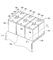
- FIG. 1 It is a perspective view which shows the electronic component mounting apparatus which is an Example of this invention. It is a top view which shows the electronic component mounting apparatus of FIG. 1 in the viewpoint from upper direction. It is a perspective view which shows the measuring device with which the electronic component mounting apparatus of FIG. 1 is provided. It is sectional drawing in the AA line shown in FIG. It is a block diagram which shows the control apparatus with which the electronic component mounting apparatus of FIG. 1 is provided. It is a side view of the measuring device which measures the electrical property of an electronic component. It is a side view of the measuring device which measures the electrical property of an electronic component. It is a table
- FIG. 1 is a perspective view of the electronic component mounting apparatus 10
- FIG. 2 is a plan view showing the electronic component mounting apparatus 10 with a cover and the like removed from a viewpoint from above.
- the electronic component mounting apparatus 10 is an apparatus for mounting electronic components on a circuit board.
- the electronic component mounting apparatus 10 has one system base 14 and two mounting machines 16 arranged side by side on the system base 14.
- the direction in which the mounting machines 16 are arranged is referred to as the X-axis direction
- the horizontal direction perpendicular to the direction is referred to as the Y-axis direction.
- Each mounting machine 16 mainly includes a mounting machine main body 20, a transport device 22, a mounting head moving device (hereinafter sometimes abbreviated as “moving device”) 24, a supply device 26, and a mounting head 28.
- the mounting machine main body 20 includes a frame portion 30 and a beam portion 32 that is overlaid on the frame portion 30.
- the transport device 22 includes two conveyor devices 40 and 42.
- the two conveyor devices 40 and 42 are disposed in the frame portion 30 so as to be parallel to each other and extend in the X-axis direction.
- Each of the two conveyor devices 40 and 42 conveys a circuit board supported by each conveyor device 40 and 42 in the X-axis direction by an electromagnetic motor (see FIG. 5) 46.
- the circuit board is fixedly held by a board holding device (see FIG. 5) 48 at a predetermined position.
- the moving device 24 is an XY robot type moving device.
- the moving device 24 includes an electromagnetic motor (see FIG. 5) 52 that slides the slider 50 in the X-axis direction and an electromagnetic motor (see FIG. 5) 54 that slides in the Y-axis direction.
- a mounting head 28 is attached to the slider 50, and the mounting head 28 moves to an arbitrary position on the frame unit 30 by the operation of the two electromagnetic motors 52 and 54.
- the supply device 26 is a feeder-type supply device, and is disposed at the front end of the frame portion 30.
- the supply device 26 has a tape feeder 70.
- the tape feeder 70 accommodates the taped component in a wound state.
- the taped component is a taped electronic component.
- the tape feeder 70 sends out the taped parts by a delivery device (see FIG. 5) 76.
- the feeder type supply device 26 supplies the electronic component at the supply position by feeding the taped component.
- the tape feeder 70 can be attached to and detached from the frame unit 30 and can cope with replacement of electronic components.
- the mounting head 28 is for mounting electronic components on the circuit board.
- the mounting head 28 has a suction nozzle 78 provided on the lower end surface.
- the suction nozzle 78 communicates with a positive / negative pressure supply device (see FIG. 5) 80 via negative pressure air and positive pressure air passages.
- the suction nozzle 78 sucks and holds the electronic component with a negative pressure, and releases the held electronic component with a positive pressure.
- the suction nozzle 78 is formed of a conductive material and is detachable from the mounting head 28.
- a suction nozzle (hereinafter, may be abbreviated as “conductive nozzle”) 78 formed of a conductive material is replaced with a suction nozzle (hereinafter, may be abbreviated as “insulation nozzle”) (which may be abbreviated as “conductive nozzle”) (See FIG. 6).
- the mounting head 28 has a nozzle lifting / lowering device 86 (see FIG. 5) 86 that lifts and lowers the conductive nozzle 78 or the insulating nozzle 82. The mounting head 28 changes the vertical position of the electronic component to be held by the nozzle lifting device 86.
- the mounting machine 16 includes a mark camera (see FIG. 5) 90 and a parts camera (see FIGS. 1 and 2) 92.
- the mark camera 90 is fixed to the lower surface of the slider 50 while facing downward.
- the slider 50 is moved by the moving device 24 so that an arbitrary position on the frame unit 30 can be imaged.
- the parts camera 92 is provided in the frame portion 30 between the transport device 22 and the supply device 26 in a state of facing upward, and images the electronic components held by the suction nozzles 78 and 82 of the mounting head 28. To do.
- a work tool station 94 is provided on the side of the parts camera 92, that is, in the frame unit 30 between the transport device 22 and the supply device 26.
- the work tool station 94 stores the insulating nozzle 82 and automatically replaces the conductive nozzle 78 mounted on the mounting head 28 with the insulating nozzle 82 stored in the work tool station 94.
- a disposal box 96 is provided on the side of the parts camera 92 opposite to the work tool station 94. The disposal box 96 is for discarding electronic components that are inappropriate to be mounted on the circuit board.
- each measuring device 100 has a plurality of probes (probes) 102.
- the plurality of probes 102 are provided on the upper surface of the measuring apparatus 100 and protrude upward.
- a plurality of electrodes of the electronic component are electrically connected to the plurality of probes 102, and a voltage is applied to the probe 102, whereby the electrical characteristics of the electronic component are detected by the detection unit (FIG. 5).
- (Ref.) 104 Specifically, the capacitance is measured for an electronic component such as a capacitor, and the resistance value is measured for an electronic component such as a resistance element or a diode.
- a plurality of probes 102 of each measuring device 100 are provided corresponding to a plurality of electrodes of the electronic component.
- two probes 102 are provided, and the distance between the two probes 102 is the distance between the two electrodes of the electronic component.
- three or more probes 102 are provided, and these three or more probes 102 are provided as electrodes of three or more electronic parts. Correspondingly, they are arranged. For this reason, the arrangement
- the identification code written on the identification plate 106 is different for each measuring device 100, and the measuring device 100 can be distinguished based on information read from the identification code.
- a reference mark 108 is written on the upper surface of each measuring device 100. As will be described in detail later, the reference mark 108 is used when an electrode of an electronic component is electrically connected to the probe 102.
- the measuring device 100 is detachably mounted on a mounting base 110 provided on the frame portion 30 between the transport device 22 and the supply device 26. Specifically, as shown in FIG. 4, a plurality of convex portions 112 are formed on the upper surface of the mounting table 110. On the other hand, a concave portion 114 having a shape corresponding to the convex portion 112 is formed on the lower surface of the measuring device 100. Then, the measuring device 100 is mounted at a predetermined position on the mounting table 110 by fitting the concave portion 114 of the measuring device 100 to the convex portion 112 of the mounting table 110.
- a magnet 116 is further fixed to the upper surface of the mounting table 110, and a magnet 118 having a magnetic pole opposite to the magnet 116 is fixed to the lower surface of the measuring apparatus 100. Then, the magnets 116 and 118 face each other by fitting the concave portion 114 of the measuring device 100 to the convex portion 112 of the mounting base 110. Thereby, the measuring device 100 is mounted on the mounting table 110 by magnetic force.
- the measuring device 100 is mounted on the mounting base 110 simply by fitting the concave portion 114 to the convex portion 112. Then, the measuring device 100 can be removed from the mounting base 110 by lifting it upward against the magnetic force. That is, the measuring device 100 can be attached to and detached from the mounting base 110 with one touch without using a tool or the like.
- the six measuring devices 100 are mounted on the mounting table 110
- the six measuring devices 100 and another measuring device 100 are also prepared, and the measuring device 100 mounted on the mounting table 110 is prepared. It is possible to detach the mounting table 110 and mount the prepared measuring device 100 on the mounting table 110.
- the arrangement of the plurality of probes 102 included in the prepared measurement apparatus 100 is different from the arrangement of the plurality of probes 102 included in the measurement apparatus 100 mounted on the mounting table 110.
- the mounting machine 16 further includes a control device 120 as shown in FIG.
- the control device 120 includes a controller 122 and a plurality of drive circuits 126.
- the plurality of drive circuits 126 are connected to the electromagnetic motors 46, 52, 54, the substrate holding device 48, the delivery device 76, the positive / negative pressure supply device 80, and the nozzle lifting / lowering device 86.
- the controller 122 includes a CPU, a ROM, a RAM, and the like, mainly a computer, and is connected to a plurality of drive circuits 126. As a result, the operations of the transport device 22, the moving device 24, and the like are controlled by the controller 122.
- the controller 122 is connected to an image processing device 128 that processes image data obtained by the mark camera 90 and the part camera 92. Thereby, the controller 122 acquires various types of information from the image data.
- the controller 122 is also connected to the detection unit 104 of each measurement apparatus 100. Thereby, the controller 122 acquires electrical characteristics such as capacitance and resistance value of the electronic component measured by the measuring apparatus 100.
- the mounting operation can be performed by the mounting head 28 on the circuit board held by the transport device 22 with the above-described configuration.
- the circuit board is transported to the work position in accordance with a command from the controller 122, and is fixedly held by the board holding device 48 at that position.
- the tape feeder 70 sends out a taped component and supplies an electronic component at a supply position in accordance with a command from the controller 122.
- the mounting head 28 moves above the supply position of the electronic component in response to a command from the controller 122 and sucks and holds the electronic component by the conductive nozzle 78.
- the mounting head 28 moves above the circuit board in accordance with a command from the controller 122 and mounts the held electronic component on the circuit board.
- the mounting head 28 sucks and holds the electronic component supplied by the tape feeder 70, and the electronic component is mounted on the circuit board.
- the display device (not shown) A screen for prompting replacement of the tape feeder 70 is displayed. The operator then replaces the tape feeder 70 according to the display screen. Thereby, it is possible to appropriately cope with replenishment and replacement of electronic components.
- the operator may mistakenly replace the tape feeder 70 in which an electronic component different from the electronic component to be mounted is accommodated.
- a component manufacturer loads and delivers an electronic component different from a regular electronic component in a component package.
- the electrical characteristics of the electronic components are measured, and whether or not the tape feeder 70 is replaced with an appropriate tape feeder 70, that is, an appropriate one. It is determined whether or not electronic parts have been replenished.
- the conductive nozzle 78 mounted on the mounting head 28 is replaced with the insulating nozzle 82.
- the mounting head 28 to which the conductive nozzle 78 is mounted moves above the work tool station 94 in accordance with a command from the controller 122, and the conductive nozzle 78 mounted to the mounting head 28 in the work tool station 94 moves to the work tool station 94.
- the insulating nozzle 82 stored in the tool station 94 is replaced.
- the mounting head 28 to which the insulating nozzle 82 is mounted moves above the supply position of the electronic component according to a command from the controller 122 and sucks and holds the electronic component by the insulating nozzle 82. Subsequently, the mounting head 28 moves above the parts camera 92 in accordance with a command from the controller 122, and images the electronic components sucked and held by the insulating nozzle 82 by the parts camera 92. This is to make the controller 122 recognize the position of the electrode of the electronic component with respect to the center of the insulating nozzle 82. The mounting head 28 moves upward of the measuring device 100 by a command from the controller 122 based on the recognition result. Then, the measuring device 100 measures the electrical characteristics of the held electronic component.
- the mounting head 28 lowers the held electronic component above the measuring device 100 by the nozzle lifting device 86.
- the plurality of electrodes 132 of the electronic component 130 held by the insulating nozzle 82 are in pressure contact with the plurality of probes 102 of the measuring apparatus 100. That is, the electrode 132 of the electronic component 130 and the probe 102 of the measuring device 100 are electrically connected.
- by pressing the electrode 132 against the probe 102 it is possible to appropriately measure electrical characteristics even when the surface of the electrode 132 is covered with an oxide film or the like.
- the electrode 132 of the electronic component 130 and the probe 102 of the measuring device 100 are electrically connected, a voltage is applied to the probe 102, and the electrical characteristics of the electronic component 130 are measured by the detection unit 104 of the measuring device 100.
- the measured electrical characteristics of the electronic component 130 are compared with the electrical characteristics of the electronic component to be replenished.
- the electrical characteristics of the electronic component differ for each type of electronic component.
- the measured electrical property of the electronic component 130 and the electrical component of the electronic component to be replenished The characteristics are different. For this reason, when the measured electrical characteristics of the electronic component 130 and the electrical characteristics of the electronic component to be replaced are different, it is determined that the wrong electronic component has been supplied, and an error screen is displayed on the display device or the like. Is done.
- the electronic component 130 whose electrical characteristics have been measured is charged. This is because a voltage is applied to the electronic component 130 held by the insulating nozzle 82. Mounting the charged electronic component 130 on the circuit board is not preferable because electricity charged in the electronic component 130 flows to the circuit board. For this reason, the electronic component whose electrical characteristics are measured is discarded in the disposal box 96.
- the mounting operation is resumed after the electronic parts whose electrical characteristics have been measured are discarded in the disposal box 96.
- the insulating nozzle 82 mounted on the mounting head 28 is replaced with the conductive nozzle 78 at the work tool station.
- the arrangement of the plurality of probes 102 of each measuring device 100 is different, and the types of electronic components 130 that can be measured by each measuring device 100 are also different. This is because the arrangement of the plurality of electrodes 132 of the electronic component 130 differs depending on the type of the electronic component 130, as can be understood by comparing FIG. 6 and FIG. For this reason, the mounting machine 16 automatically identifies the types of electronic components 130 that can be measured by each measuring device 100.
- the identification plate 106 for identifying each measurement device 100 is attached to each measurement device 100.
- the identification plate 106 is imaged by the mark camera 90, and the imaged data is processed by the image processing device 128.
- the controller 122 acquires the device number of each measuring device 100.
- This device number is merely a symbol for distinguishing each measuring device 100, and may be a simple number such as “01”, “02”, etc., and a number such as “A1”, “B2” and the alphabet. It may be combined with.
- the controller 122 stores the device number and the type of the electronic component 130 that can be measured by the measuring device 100 of the device number in association with each other. Specifically, map data corresponding to FIG. 8 is stored.
- numbers such as “01” and “02” are adopted as device numbers, and for each device number, a target component that is an electronic component 130 that can be measured by the device number measuring device 100 is stored.
- the numbers described in the “target component” column are numbers indicating the dimensions of the electronic component 130.
- “1608” generally has a long side of 1.6 mm and a short side of 0.8 mm.
- a rectangular electronic component is shown. That is, the measuring device 100 having the device number “01” can measure the electrical characteristics of a generally rectangular electronic component having a long side of 1.6 mm and a short side of 0.8 mm.
- the controller 122 acquires the types of electronic components 130 that can be measured by each measuring device 100 based on the device number obtained by imaging the identification plate 106 and the map data corresponding to FIG. Thus, in the mounting machine 16, the type of the electronic component 130 that can be measured by each measuring device 100 is automatically identified. This makes it possible to efficiently measure the electrical characteristics of the electronic component.
- the controller 122 includes a component type identification unit 140 as a functional unit for automatically identifying the type of the electronic component 130 that can be measured by each measurement apparatus 100, as shown in FIG. Furthermore, the component type identification unit 140 includes a component type storage unit 142 as a functional unit that stores map data corresponding to FIG.
- ⁇ Relative position of probe and reference mark> the electronic component 130 is very small, and the electrode 132 of the electronic component 130 is even smaller. For this reason, when the probe 102 of the measuring device 100 and the electrode 132 of the electronic component 130 are brought into contact with each other, it is necessary to perform fine position control. For this reason, a reference mark 108 is written on the upper surface of each measuring apparatus 100, and position control is performed with reference to the reference mark 108 when the probe 102 and the electrode 132 are brought into contact with each other. Since the distance between the reference mark 108 and the probe 102 is relatively short, appropriate position control can be performed.
- the relative positional relationship between the probe 102 and the reference mark 108 is naturally necessary.
- the relative position relationship between the probe 102 and the reference mark 108 is also automatically acquired by the mounting machine 16.
- the controller 122 stores the device number obtained by imaging the identification plate 106 and the relative positional relationship between the probe 102 and the reference mark 108 in the measuring device 100 of the device number in association with each other. Yes. Specifically, map data corresponding to FIG. 8 is stored. In the figure, the relative positional relationship between the probe 102 and the reference mark 108 is stored for each device number.
- the numbers described in the “relative position” column are numbers indicating the distances in the X-axis direction and the Y-axis direction between the probe 102 and the reference mark 108 that are positions where the insulating nozzle 82 stops for measurement.
- X: XX, Y: XX indicates that the distance between the probe 102 and the reference mark 108 in the X-axis direction is XX mm, and the distance in the X-axis direction is XX mm. ing.
- the controller 122 acquires the distance between the probe 102 and the reference mark 108 in the X-axis direction and the Y-axis direction based on the device number obtained by imaging the identification plate 106 and the map data corresponding to FIG. .
- the relative positional relationship between the probe 102 and the reference mark 108 in each measurement apparatus 100 is automatically acquired. Accordingly, it is possible to perform appropriate position control and appropriately measure the electrical characteristics of the electronic component.
- the controller 122 has a relative position acquisition unit 144 as shown in FIG. is doing. Furthermore, the relative position acquisition unit 144 includes a relative position storage unit 146 as a functional unit that stores map data corresponding to FIG.
- ⁇ Replacement of measuring device> when the type of circuit board to be manufactured is exchanged, the electronic component to be mounted is also exchanged. At this time, the electrical characteristics of the newly replaced electronic component may not be measured by each measuring device 100 mounted on the mounting table 110. That is, the type of electronic component that can be measured by each measuring device 100 mounted on the mounting table 110 may be different from the type of electronic component that is newly replaced. In such a case, the user can mount the measuring device 100 capable of measuring the electrical characteristics of the newly replaced electronic component on the mounting base 110.
- the measuring device 100 can be attached to and detached from the mounting table 110 with one touch.
- the measuring device 100 is prepared, and the arrangement of the plurality of probes 102 included in the prepared measuring device 100 is mounted on the mounting table 110. This is different from the arrangement of the plurality of probes 102 included in the measuring device 100. That is, the measuring device 100 capable of measuring the electrical characteristics of the newly replaced electronic component is prepared separately from the six measuring devices 100 mounted on the mounting base 110.
- the user removes the measuring device 100 that can measure the electrical characteristics of the electronic components that are not necessary for manufacturing a new circuit board from the mounting base 110 and replaces the measuring device 100 with a new one. It is possible to attach a measuring device 100 capable of measuring the electrical characteristics of electronic components. As described above, it is possible to deal with a plurality of types of electronic components by exchanging the measuring device 100 according to the types of the electronic components.
- the number of uses of the measuring device 100 is managed, and an instruction for maintenance work is notified to the worker according to the number of uses.
- the controller 122 the number of uses of the measuring device 100 and the maintenance history are stored for each measuring device 100. Each time each measuring device 100 is used, the number of uses of each measuring device 100 is updated. When updating the number of uses, the number of uses of the measuring device 100 corresponding to the device number obtained by imaging the identification plate 106 is updated.
- the controller 122 stores a preset use limit number for each measuring device 100. This use limit number is the number of times set in consideration of wear of the probe 102 of each measuring device 100 or the like. Then, the controller 122 compares the number of times of use of the measuring device 100 with the number of times of use limit for each measuring device 100. When the number of times of use reaches the number of times of use limit, the maintenance work instruction is notified to the operator. The Accordingly, the operator can maintain the measurement accuracy of the measurement device 100 by removing the measurement device 100 from the mounting base 110 and performing maintenance work such as replacement and cleaning of the probe 102 in accordance with the notification. Become.
- the controller 122 is a maintenance judgment as a functional unit for judging whether or not the maintenance work should be executed by comparing the number of times of use in each measuring device 100 and the number of times of use limit. Part 150. Furthermore, the maintenance determination unit 150 includes a usage count storage unit 152 as a functional unit that stores the usage count of each measuring device 100.
- the mounting machine 16 is an example of an electronic component mounting machine.
- the mounting head 28 is an example of a mounting head.
- the conductive nozzle 78 is an example of a conductive nozzle.
- the insulating nozzle 82 is an example of an insulating nozzle.
- the mark camera 90 is an example of an imaging device.
- the disposal box 96 is an example of a disposal apparatus.
- the measuring device 100 is an example of a measuring device.
- the probe 102 is an example of a device side electrode and a probe.
- the identification plate 106 is an example of an identification symbol.
- the reference mark 108 is an example of a reference mark.
- the mounting table 110 is an example of a mounting unit.
- the electronic component 130 is an example of an electronic component.
- the electrode 132 is an example of a component side electrode.
- the component type identification unit 140 is an example of an identification device.
- the component type storage unit 142 is an example of a component type storage unit.
- the relative position acquisition unit 144 is an example of a relative position acquisition device.
- the relative position storage unit 146 is an example of a relative position storage unit.
- the process of holding the electronic component 130 by the insulating nozzle 82 is an example of the electronic component holding process.
- the process of measuring the electrical characteristics of the electronic component 130 by the measuring apparatus 100 is an example of a measurement process.
- the process of discarding the electronic component whose electrical characteristics are measured in the disposal box 96 is an example of the disposal process.
- this invention is not limited to the said Example, It is possible to implement in the various aspect which gave various change and improvement based on the knowledge of those skilled in the art. Specifically, for example, in the above embodiment, the electrical characteristics of the electronic component are measured in order to determine whether or not the electronic component is properly replenished, but whether or not the electronic component is normal. In order to determine this, the electrical characteristics of the electronic component may be measured.
- the concave portion 114 is fitted to the convex portion 112 and the measuring device 100 is attached to the mounting table 110 by magnetic force.
- the measuring device 100 can be mounted on the mounting table 110.
- the measuring device 100 can be mounted on the mounting base 110 by a lock mechanism using a spring or the like.
- the measuring device 100 can be mounted on the mounting table 110 with a bolt or the like. That is, the measuring device 100 can be mounted on the mounting table 110 using a tool or the like.
- the device number of each measuring device 100 is acquired by imaging the identification plate 106, and the electronic component 130 that can be measured by the measuring device 100 based on the map data stored in the controller 122.
- the type and the relative position between the probe 102 and the reference mark 108 in each measuring device 100 are acquired.
- the reference mark 108 is written on the measuring device 100 that can be attached to and detached from the mounting base 110.
- the measuring device 100 that is fixed to the frame unit 30, that is, the non-replaceable measuring device 100 is used.
- the reference mark 108 may be written.
- very precise positioning is required.
- the moving device 24 that moves the mounting head 28 moves for a long time and there is a risk of thermal deformation
- the moving device 24 is calibrated, the amount of deformation is recognized, and the moving distance of the mounting head is adjusted. .
- the adjustment amount of the movement distance when the mounting head 28 aligns the electrode of the electronic component with the probe 102 can be obtained with higher accuracy.
- Mounting machine 28 Mounting head 78: Conductive nozzle 82: Insulating nozzle 90: Mark camera (imaging device) 96: Disposal box (disposal device) 100: Measuring device 102: Probe (device side electrode) 106: Identification plate (identification) Symbol) 108: Reference mark 110: Mounting base (mounting part) 130: Electronic component 132: Electrode (part side electrode) 140: Part type identification part (identification device) 142: Part type storage part 144: Relative position acquisition part (relative) Position acquisition device) 146: Relative position storage unit
Landscapes
- Engineering & Computer Science (AREA)
- Microelectronics & Electronic Packaging (AREA)
- Manufacturing & Machinery (AREA)
- Operations Research (AREA)
- Environmental & Geological Engineering (AREA)
- Computer Hardware Design (AREA)
- General Engineering & Computer Science (AREA)
- Physics & Mathematics (AREA)
- General Physics & Mathematics (AREA)
- Supply And Installment Of Electrical Components (AREA)
- Testing Electric Properties And Detecting Electric Faults (AREA)
Abstract
Description
図1および図2に、電子部品装着装置10を示す。図1は、電子部品装着装置10の斜視図であり、図2は、カバー等を外した状態の電子部品装着装置10を上方からの視点で示した平面図である。電子部品装着装置10は、回路基板に電子部品を実装するための装置である。電子部品装着装置10は、1つのシステムベース14と、そのシステムベース14の上に並んで配設された2つの装着機16とを有している。なお、以下の説明では、装着機16の並ぶ方向をX軸方向と称し、その方向に直角な水平の方向をY軸方向と称する。
装着機16では、上述した構成によって、搬送装置22に保持された回路基板に対して、装着ヘッド28によって装着作業を行うことが可能とされている。具体的には、コントローラ122の指令により、回路基板が作業位置まで搬送され、その位置において、基板保持装置48によって固定的に保持される。また、テープフィーダ70は、コントローラ122の指令により、テープ化部品を送り出し、電子部品を供給位置において供給する。そして、装着ヘッド28が、コントローラ122の指令により、電子部品の供給位置の上方に移動し、導電ノズル78によって電子部品を吸着保持する。続いて、装着ヘッド28は、コントローラ122の指令により、回路基板の上方に移動し、保持している電子部品を回路基板上に装着する。
装着機16では、上述したように、テープフィーダ70によって供給された電子部品を、装着ヘッド28が吸着保持し、その電子部品が回路基板上に装着される。このように構成された装着機16では、電子部品の供給不足を回避するべく、テープフィーダ70に収容されている電子部品数が所定数より少なくなった場合に、表示装置(図示省略)に、テープフィーダ70の交換等を促すための画面が表示される。そして、作業者は、表示画面に従って、テープフィーダ70の交換等を行う。これにより、電子部品の補給,交換等に適切に対応することが可能となる。
また、各計測装置100の複数のプローブ102の配置は、上述したように、異なっており、各計測装置100で計測可能な電子部品130の種類も異なる。これは、図6と図7とを比較して解るように、電子部品130の種類毎に、電子部品130の複数の電極132の配置が異なっているためである。このため、装着機16では、各計測装置100で計測可能な電子部品130の種類が、自動で識別される。
また、電子部品130は非常に小さく、電子部品130の電極132は、さらに小さい。このため、計測装置100のプローブ102と電子部品130の電極132とを接触させる際には、細やかな位置制御を行う必要がある。このため、各計測装置100の上面には、基準マーク108が記されており、プローブ102と電極132とを接触させる際に、基準マーク108を基準とした位置制御が行われる。基準マーク108とプローブ102との間の距離は比較的短いため、適切な位置制御を行うことが可能となる。
また、製造すべき回路基板の種類が交換される際には、装着すべき電子部品も交換される。この際、装着台110に装着されている各計測装置100で、新たに交換された電子部品の電気的特性を計測することができない場合がある。つまり、装着台110に装着されている各計測装置100で計測可能な電子部品の種類と、新たに交換された電子部品の種類とが、異なる場合がある。このような場合には、ユーザは、新たに交換された電子部品の電気的特性を計測可能な計測装置100を装着台110に装着することが可能である。
また、装着機16では、計測装置100の使用回数が管理されており、使用回数に応じてメンテナンス作業の指示が、作業者に通知される。詳しくは、コントローラ122において、計測装置100毎に、計測装置100の使用回数とメンテナンス履歴とが記憶されている。そして、各計測装置100が使用される度に、各計測装置100の使用回数が更新される。なお、使用回数更新時には、識別プレート106の撮像により得られる装置ナンバーに応じた計測装置100の使用回数が更新される。
Claims (13)
- 回路基板に電子部品を装着する電子部品装着機において、
当該電子部品装着機が、
それぞれが、電子部品の複数の部品側電極に対応する複数の装置側電極を有し、それら複数の装置側電極が前記複数の部品側電極に電気的に接続されることで、電子部品の電気的特性を計測する複数の計測装置と、
それら複数の計測装置のうちの任意の計測装置が装着される装着部と
を備え、
前記複数の計測装置の各々の前記複数の装置側電極の配置が、異なっており、
前記装着部に装着されている前記任意の計測装置の替わりに、前記複数の計測装置のうちの前記任意の計測装置以外の計測装置を、前記装着部に装着可能であることを特徴とする電子部品装着機。 - 前記装置側電極が、
プローブであることを特徴とする請求項1に記載の電子部品装着機。 - 当該電子部品装着機が、
前記計測装置に記された識別記号を撮像する撮像装置と、
前記撮像装置によって撮像された前記識別記号の撮像データに基づいて、前記計測装置を識別する識別装置と
を備えることを特徴とする請求項1または請求項2に記載の電子部品装着機。 - 前記識別装置が、
前記計測装置によって計測可能な電子部品の種類と前記識別記号の撮像データとを関連付けて記憶する部品種記憶部を有し、前記部品種記憶部に記憶されているデータに基づいて、前記計測装置によって計測可能な電子部品の種類を識別することを特徴とする請求項3に記載の電子部品装着機。 - 前記識別記号が、
前記計測装置によって計測可能な電子部品の種類を識別するための記号であり、
前記識別装置が、
前記識別記号の撮像データに基づいて、前記計測装置によって計測可能な電子部品の種類を識別することを特徴とする請求項3に記載の電子部品装着機。 - 前記複数の装置側電極の各々との相対的な位置を示すための基準マークが、前記計測装置に記されていることを特徴とする請求項1ないし請求項5のいずれか1つに記載の電子部品装着機。
- 当該電子部品装着機が、
前記計測装置に記された識別記号を撮像する撮像装置と、
前記基準マークと前記複数の装置側電極の各々との相対的な位置に関する相対位置情報と、前記撮像装置によって撮像された前記識別記号の撮像データとを関連付けて記憶する相対位置記憶部を有し、その相対位置記憶部に記憶されているデータに基づいて前記相対位置情報を取得する相対位置取得装置と
を備えることを特徴とする請求項6に記載の電子部品装着機。 - 当該電子部品装着機が、
前記計測装置に記された識別記号であって、前記基準マークと前記複数の装置側電極の各々との相対的な位置に関する相対位置情報を含む記号を撮像する撮像装置と、
前記撮像装置によって撮像された前記識別記号の撮像データに基づいて、前記相対位置情報を取得する相対位置取得装置と
を備えることを特徴とする請求項6に記載の電子部品装着機。 - 当該電子部品装着機は、複数の前記装着部を備え、
前記計測装置が、
前記複数の装着部のうちの任意のものに装着されることを特徴とする請求項1ないし請求項8のいずれか1つに記載の電子部品装着機。 - 前記計測装置が、
前記装着部に、工具を使用せずに、ワンタッチで着脱可能に装着されることを特徴とする請求項1ないし請求項9のいずれか1つに記載の電子部品装着機。 - 回路基板に電子部品を装着する電子部品装着機において、
当該電子部品装着機が、
電子部品の複数の部品側電極に対応する複数の装置側電極を有し、それら複数の装置側電極が前記複数の部品側電極に電気的に接続されることで、電子部品の電気的特性を計測する計測装置と、
その計測装置が装着される装着部と
を備え、
前記計測装置が、
前記装着部に、工具を使用せずに、ワンタッチで着脱可能に装着されることを特徴とする電子部品装着機。 - 回路基板に電子部品を装着する電子部品装着機において、
当該電子部品装着機が、
電子部品の複数の部品側電極に対応する複数の装置側電極を有し、それら複数の装置側電極が前記複数の部品側電極に電気的に接続されることで、電子部品の電気的特性を計測する計測装置を備え、
前記複数の装置側電極の各々との相対的な位置を示すための基準マークが、前記計測装置に記されていることを特徴とする電子部品装着機。 - 導電性部材により成形された導電ノズルを有する装着ヘッドと、
電子部品を廃棄する廃棄装置と、
電子部品の複数の部品側電極に対応する複数の装置側電極を有し、それら複数の装置側電極が前記複数の部品側電極に電気的に接続されることで、電子部品の電気的特性を計測する計測装置と
を備え、前記導電ノズルによって保持された電子部品を回路基板に装着する電子部品装着機で、前記計測装置によって電子部品の電気的特性を計測する計測方法において、
前記装着ヘッドが、
絶縁性部材により成形された絶縁ノズルを有し、
当該計測方法が、
前記絶縁ノズルによって電子部品を保持する電子部品保持工程と、
電子部品保持工程で前記絶縁ノズルに保持された電子部品の前記複数の部品側電極に、前記複数の装置側電極を電気的に接続することで、電子部品の電気的特性を計測する計測工程と、
前記計測工程で電気的特性が計測された電子部品を、前記廃棄装置に廃棄する廃棄工程と
を含むことを特徴とする計測方法。
Priority Applications (5)
| Application Number | Priority Date | Filing Date | Title |
|---|---|---|---|
| EP20167946.1A EP3712627B1 (en) | 2013-03-29 | 2013-03-29 | Electronic component mounting machine and measurement method |
| PCT/JP2013/059480 WO2014155657A1 (ja) | 2013-03-29 | 2013-03-29 | 電子部品装着機および計測方法 |
| CN201380075258.1A CN105075422B (zh) | 2013-03-29 | 2013-03-29 | 电子元件安装机及计测方法 |
| JP2015507863A JP6234437B2 (ja) | 2013-03-29 | 2013-03-29 | 電子部品装着機および計測方法 |
| EP13880038.8A EP2981164B1 (en) | 2013-03-29 | 2013-03-29 | Electronic component mounting machine and measurement method |
Applications Claiming Priority (1)
| Application Number | Priority Date | Filing Date | Title |
|---|---|---|---|
| PCT/JP2013/059480 WO2014155657A1 (ja) | 2013-03-29 | 2013-03-29 | 電子部品装着機および計測方法 |
Publications (1)
| Publication Number | Publication Date |
|---|---|
| WO2014155657A1 true WO2014155657A1 (ja) | 2014-10-02 |
Family
ID=51622722
Family Applications (1)
| Application Number | Title | Priority Date | Filing Date |
|---|---|---|---|
| PCT/JP2013/059480 Ceased WO2014155657A1 (ja) | 2013-03-29 | 2013-03-29 | 電子部品装着機および計測方法 |
Country Status (4)
| Country | Link |
|---|---|
| EP (2) | EP2981164B1 (ja) |
| JP (1) | JP6234437B2 (ja) |
| CN (1) | CN105075422B (ja) |
| WO (1) | WO2014155657A1 (ja) |
Cited By (18)
| Publication number | Priority date | Publication date | Assignee | Title |
|---|---|---|---|---|
| JP2017026325A (ja) * | 2015-07-15 | 2017-02-02 | 富士機械製造株式会社 | 検査装置 |
| JP2018098422A (ja) * | 2016-12-15 | 2018-06-21 | 株式会社Fuji | 部品特性測定装置 |
| JP2018174249A (ja) * | 2017-03-31 | 2018-11-08 | ヤマハ発動機株式会社 | 部品実装装置 |
| US10470351B2 (en) | 2015-06-17 | 2019-11-05 | Fuji Corporation | Mounting system |
| JPWO2018150482A1 (ja) * | 2017-02-15 | 2019-11-07 | 株式会社Fuji | 測定装置、測定方法 |
| US10509069B2 (en) | 2015-07-15 | 2019-12-17 | Fuji Corporation | Inspection device |
| US10551410B2 (en) | 2015-07-15 | 2020-02-04 | Fuji Corporation | Inspection device |
| JP2020064886A (ja) * | 2018-10-15 | 2020-04-23 | パナソニックIpマネジメント株式会社 | 特性計測装置、部品実装装置、特性計測方法および部品実装方法 |
| JP2021044577A (ja) * | 2020-12-02 | 2021-03-18 | 株式会社Fuji | 電気的特性測定方法 |
| JP2021077908A (ja) * | 2021-02-02 | 2021-05-20 | 株式会社Fuji | 装着機 |
| WO2021100304A1 (ja) * | 2019-11-18 | 2021-05-27 | パナソニックIpマネジメント株式会社 | 部品実装システムおよび実装ヘッドならびに部品実装方法 |
| JPWO2021149175A1 (ja) * | 2020-01-22 | 2021-07-29 | ||
| JP2021170684A (ja) * | 2020-03-30 | 2021-10-28 | 株式会社Fuji | 装着機 |
| JP2022016456A (ja) * | 2016-06-14 | 2022-01-21 | 株式会社Fuji | 電気的特性取得装置 |
| JP2022167994A (ja) * | 2018-10-15 | 2022-11-04 | パナソニックIpマネジメント株式会社 | 部品実装装置および部品実装方法 |
| JPWO2023073840A1 (ja) * | 2021-10-27 | 2023-05-04 | ||
| CN117368574A (zh) * | 2023-11-03 | 2024-01-09 | 无锡卓海科技股份有限公司 | 电阻测量仪的使用方法 |
| JP2024177509A (ja) * | 2022-10-05 | 2024-12-19 | 株式会社Fuji | 装着機 |
Families Citing this family (4)
| Publication number | Priority date | Publication date | Assignee | Title |
|---|---|---|---|---|
| JP7015780B2 (ja) * | 2016-06-14 | 2022-02-03 | 株式会社Fuji | 電気的特性取得装置 |
| JP7281620B2 (ja) * | 2018-10-15 | 2023-05-26 | パナソニックIpマネジメント株式会社 | 特性計測装置、部品実装装置、特性計測方法および部品実装方法 |
| EP3687271A1 (en) | 2019-01-25 | 2020-07-29 | Mycronic AB | Eletrical verification of electronic components |
| WO2020157971A1 (ja) * | 2019-02-01 | 2020-08-06 | 株式会社Fuji | 作業機 |
Citations (2)
| Publication number | Priority date | Publication date | Assignee | Title |
|---|---|---|---|---|
| JP2005303143A (ja) * | 2004-04-14 | 2005-10-27 | Fuji Mach Mfg Co Ltd | テープ化電子回路部品接続装置 |
| JP2011159964A (ja) | 2010-01-06 | 2011-08-18 | Juki Corp | 電子部品実装装置 |
Family Cites Families (9)
| Publication number | Priority date | Publication date | Assignee | Title |
|---|---|---|---|---|
| JP2522922Y2 (ja) * | 1990-06-01 | 1997-01-22 | 日本電気株式会社 | アタッチメント交換機構 |
| US5443534A (en) * | 1992-07-21 | 1995-08-22 | Vlt Corporation | Providing electronic components for circuity assembly |
| JPH07263517A (ja) * | 1994-03-24 | 1995-10-13 | Hitachi Electron Eng Co Ltd | Icソケットの位置決め装置 |
| JP4562254B2 (ja) * | 1999-07-27 | 2010-10-13 | 東レエンジニアリング株式会社 | チップ実装装置及びそれにおけるキャリブレーション方法 |
| JP2005183643A (ja) * | 2003-12-19 | 2005-07-07 | Juki Corp | 電子部品認識方法及び装置 |
| CN102118961B (zh) * | 2010-01-06 | 2015-09-16 | Juki株式会社 | 电子部件安装装置 |
| JP5584651B2 (ja) * | 2011-05-12 | 2014-09-03 | ヤマハ発動機株式会社 | 吸着状態検査装置、表面実装機及び部品試験装置 |
| JP5627552B2 (ja) * | 2011-10-06 | 2014-11-19 | 日置電機株式会社 | 電子部品搭載装置および電子部品搭載方法 |
| KR101230596B1 (ko) * | 2012-03-09 | 2013-02-06 | 미래산업 주식회사 | 전자부품 공급장치, 전자부품 공급방법 및 전자부품 실장방법 |
-
2013
- 2013-03-29 CN CN201380075258.1A patent/CN105075422B/zh active Active
- 2013-03-29 JP JP2015507863A patent/JP6234437B2/ja active Active
- 2013-03-29 EP EP13880038.8A patent/EP2981164B1/en active Active
- 2013-03-29 EP EP20167946.1A patent/EP3712627B1/en active Active
- 2013-03-29 WO PCT/JP2013/059480 patent/WO2014155657A1/ja not_active Ceased
Patent Citations (2)
| Publication number | Priority date | Publication date | Assignee | Title |
|---|---|---|---|---|
| JP2005303143A (ja) * | 2004-04-14 | 2005-10-27 | Fuji Mach Mfg Co Ltd | テープ化電子回路部品接続装置 |
| JP2011159964A (ja) | 2010-01-06 | 2011-08-18 | Juki Corp | 電子部品実装装置 |
Non-Patent Citations (1)
| Title |
|---|
| See also references of EP2981164A4 |
Cited By (32)
| Publication number | Priority date | Publication date | Assignee | Title |
|---|---|---|---|---|
| US10470351B2 (en) | 2015-06-17 | 2019-11-05 | Fuji Corporation | Mounting system |
| US10509069B2 (en) | 2015-07-15 | 2019-12-17 | Fuji Corporation | Inspection device |
| JP2017026325A (ja) * | 2015-07-15 | 2017-02-02 | 富士機械製造株式会社 | 検査装置 |
| US10551410B2 (en) | 2015-07-15 | 2020-02-04 | Fuji Corporation | Inspection device |
| JP2022016456A (ja) * | 2016-06-14 | 2022-01-21 | 株式会社Fuji | 電気的特性取得装置 |
| JP7223825B2 (ja) | 2016-06-14 | 2023-02-16 | 株式会社Fuji | 電気的特性取得装置 |
| JP2018098422A (ja) * | 2016-12-15 | 2018-06-21 | 株式会社Fuji | 部品特性測定装置 |
| JPWO2018150482A1 (ja) * | 2017-02-15 | 2019-11-07 | 株式会社Fuji | 測定装置、測定方法 |
| JP2018174249A (ja) * | 2017-03-31 | 2018-11-08 | ヤマハ発動機株式会社 | 部品実装装置 |
| JP2020064886A (ja) * | 2018-10-15 | 2020-04-23 | パナソニックIpマネジメント株式会社 | 特性計測装置、部品実装装置、特性計測方法および部品実装方法 |
| JP2022167994A (ja) * | 2018-10-15 | 2022-11-04 | パナソニックIpマネジメント株式会社 | 部品実装装置および部品実装方法 |
| JP7142208B2 (ja) | 2018-10-15 | 2022-09-27 | パナソニックIpマネジメント株式会社 | 特性計測装置、部品実装装置、特性計測方法および部品実装方法 |
| JP7422294B2 (ja) | 2018-10-15 | 2024-01-26 | パナソニックIpマネジメント株式会社 | 部品実装装置および部品実装方法 |
| JP7535737B2 (ja) | 2019-11-18 | 2024-08-19 | パナソニックIpマネジメント株式会社 | 部品実装システムおよび実装ヘッドならびに部品実装方法 |
| JPWO2021100304A1 (ja) * | 2019-11-18 | 2021-05-27 | ||
| WO2021100304A1 (ja) * | 2019-11-18 | 2021-05-27 | パナソニックIpマネジメント株式会社 | 部品実装システムおよび実装ヘッドならびに部品実装方法 |
| JP7504134B2 (ja) | 2020-01-22 | 2024-06-21 | 株式会社Fuji | 実装機 |
| JPWO2021149175A1 (ja) * | 2020-01-22 | 2021-07-29 | ||
| JP2021170684A (ja) * | 2020-03-30 | 2021-10-28 | 株式会社Fuji | 装着機 |
| JP7035256B2 (ja) | 2020-03-30 | 2022-03-14 | 株式会社Fuji | 装着機 |
| JP7078698B2 (ja) | 2020-12-02 | 2022-05-31 | 株式会社Fuji | 電気的特性測定方法 |
| JP2021044577A (ja) * | 2020-12-02 | 2021-03-18 | 株式会社Fuji | 電気的特性測定方法 |
| JP7013599B2 (ja) | 2021-02-02 | 2022-01-31 | 株式会社Fuji | 装着機 |
| JP7013617B2 (ja) | 2021-02-02 | 2022-01-31 | 株式会社Fuji | 装着機 |
| JP2022003697A (ja) * | 2021-02-02 | 2022-01-11 | 株式会社Fuji | 装着機 |
| JP2021077908A (ja) * | 2021-02-02 | 2021-05-20 | 株式会社Fuji | 装着機 |
| JPWO2023073840A1 (ja) * | 2021-10-27 | 2023-05-04 | ||
| WO2023073840A1 (ja) * | 2021-10-27 | 2023-05-04 | ヤマハ発動機株式会社 | 電気特性測定装置、部品実装装置および電気特性測定方法 |
| JP7571311B2 (ja) | 2021-10-27 | 2024-10-22 | ヤマハ発動機株式会社 | 電気特性測定装置、部品実装装置および電気特性測定方法 |
| JP2024177509A (ja) * | 2022-10-05 | 2024-12-19 | 株式会社Fuji | 装着機 |
| JP7804030B2 (ja) | 2022-10-05 | 2026-01-21 | 株式会社Fuji | 装着機 |
| CN117368574A (zh) * | 2023-11-03 | 2024-01-09 | 无锡卓海科技股份有限公司 | 电阻测量仪的使用方法 |
Also Published As
| Publication number | Publication date |
|---|---|
| CN105075422B (zh) | 2018-03-27 |
| EP3712627B1 (en) | 2023-05-24 |
| EP2981164B1 (en) | 2020-07-08 |
| EP3712627A1 (en) | 2020-09-23 |
| JPWO2014155657A1 (ja) | 2017-02-16 |
| EP2981164A4 (en) | 2017-01-25 |
| EP2981164A1 (en) | 2016-02-03 |
| CN105075422A (zh) | 2015-11-18 |
| JP6234437B2 (ja) | 2017-11-22 |
Similar Documents
| Publication | Publication Date | Title |
|---|---|---|
| JP6234437B2 (ja) | 電子部品装着機および計測方法 | |
| CN102238862B (zh) | 支撑销装置、支撑销配置方法和配置装置 | |
| JP5751584B2 (ja) | 電子部品実装装置 | |
| CN110023773B (zh) | 测试系统 | |
| JP6057997B2 (ja) | 部品実装ライン | |
| JP6498764B2 (ja) | 実装システム | |
| JP6735768B2 (ja) | 実装機 | |
| JP6285697B2 (ja) | 電子部品検査装置及び電子部品実装装置 | |
| EP3032933A1 (en) | Electronic component mounting machine and transfer confirmation method | |
| JP2010131792A (ja) | スクリーン印刷装置 | |
| CN104285508A (zh) | 部件安装装置 | |
| JP5799206B2 (ja) | 実装部品検査装置、部品実装システム及び部品実装方法 | |
| CN101677507B (zh) | 用于识别并处理电子部件的信息的设备 | |
| EP2953439B1 (en) | Electronic component mounting system and electronic component mounting method | |
| JP6182505B2 (ja) | 実装荷重測定装置 | |
| JP2017027989A (ja) | 部品厚み測定方法および部品実装装置 | |
| KR101399540B1 (ko) | 검사 장치 | |
| WO2021084704A1 (ja) | 部品供給装置 | |
| JPWO2018158948A1 (ja) | 作業機、および装着方法 | |
| JP2018174249A (ja) | 部品実装装置 | |
| JP6742501B2 (ja) | 荷重計測システム | |
| JPWO2016181434A1 (ja) | 確認方法 | |
| JP7418142B2 (ja) | 対基板作業機、および異物検出方法 | |
| JP6902346B2 (ja) | 部品特性測定装置 | |
| JP7531152B2 (ja) | 方法および部品装着装置 |
Legal Events
| Date | Code | Title | Description |
|---|---|---|---|
| WWE | Wipo information: entry into national phase |
Ref document number: 201380075258.1 Country of ref document: CN |
|
| 121 | Ep: the epo has been informed by wipo that ep was designated in this application |
Ref document number: 13880038 Country of ref document: EP Kind code of ref document: A1 |
|
| ENP | Entry into the national phase |
Ref document number: 2015507863 Country of ref document: JP Kind code of ref document: A |
|
| WWE | Wipo information: entry into national phase |
Ref document number: 2013880038 Country of ref document: EP |
|
| NENP | Non-entry into the national phase |
Ref country code: DE |