WO2014156914A1 - Iii族窒化物基板の処理方法およびエピタキシャル基板の製造方法 - Google Patents
Iii族窒化物基板の処理方法およびエピタキシャル基板の製造方法 Download PDFInfo
- Publication number
- WO2014156914A1 WO2014156914A1 PCT/JP2014/057649 JP2014057649W WO2014156914A1 WO 2014156914 A1 WO2014156914 A1 WO 2014156914A1 JP 2014057649 W JP2014057649 W JP 2014057649W WO 2014156914 A1 WO2014156914 A1 WO 2014156914A1
- Authority
- WO
- WIPO (PCT)
- Prior art keywords
- iii nitride
- group iii
- substrate
- nitride substrate
- epitaxial
- Prior art date
- Legal status (The legal status is an assumption and is not a legal conclusion. Google has not performed a legal analysis and makes no representation as to the accuracy of the status listed.)
- Ceased
Links
Images


Classifications
-
- C—CHEMISTRY; METALLURGY
- C30—CRYSTAL GROWTH
- C30B—SINGLE-CRYSTAL GROWTH; UNIDIRECTIONAL SOLIDIFICATION OF EUTECTIC MATERIAL OR UNIDIRECTIONAL DEMIXING OF EUTECTOID MATERIAL; REFINING BY ZONE-MELTING OF MATERIAL; PRODUCTION OF A HOMOGENEOUS POLYCRYSTALLINE MATERIAL WITH DEFINED STRUCTURE; SINGLE CRYSTALS OR HOMOGENEOUS POLYCRYSTALLINE MATERIAL WITH DEFINED STRUCTURE; AFTER-TREATMENT OF SINGLE CRYSTALS OR A HOMOGENEOUS POLYCRYSTALLINE MATERIAL WITH DEFINED STRUCTURE; APPARATUS THEREFOR
- C30B25/00—Single-crystal growth by chemical reaction of reactive gases, e.g. chemical vapour-deposition growth
- C30B25/02—Epitaxial-layer growth
- C30B25/18—Epitaxial-layer growth characterised by the substrate
- C30B25/186—Epitaxial-layer growth characterised by the substrate being specially pre-treated by, e.g. chemical or physical means
-
- C—CHEMISTRY; METALLURGY
- C30—CRYSTAL GROWTH
- C30B—SINGLE-CRYSTAL GROWTH; UNIDIRECTIONAL SOLIDIFICATION OF EUTECTIC MATERIAL OR UNIDIRECTIONAL DEMIXING OF EUTECTOID MATERIAL; REFINING BY ZONE-MELTING OF MATERIAL; PRODUCTION OF A HOMOGENEOUS POLYCRYSTALLINE MATERIAL WITH DEFINED STRUCTURE; SINGLE CRYSTALS OR HOMOGENEOUS POLYCRYSTALLINE MATERIAL WITH DEFINED STRUCTURE; AFTER-TREATMENT OF SINGLE CRYSTALS OR A HOMOGENEOUS POLYCRYSTALLINE MATERIAL WITH DEFINED STRUCTURE; APPARATUS THEREFOR
- C30B29/00—Single crystals or homogeneous polycrystalline material with defined structure characterised by the material or by their shape
- C30B29/10—Inorganic compounds or compositions
- C30B29/40—AIIIBV compounds wherein A is B, Al, Ga, In or Tl and B is N, P, As, Sb or Bi
- C30B29/403—AIII-nitrides
-
- H—ELECTRICITY
- H10—SEMICONDUCTOR DEVICES; ELECTRIC SOLID-STATE DEVICES NOT OTHERWISE PROVIDED FOR
- H10P—GENERIC PROCESSES OR APPARATUS FOR THE MANUFACTURE OR TREATMENT OF DEVICES COVERED BY CLASS H10
- H10P14/00—Formation of materials, e.g. in the shape of layers or pillars
- H10P14/20—Formation of materials, e.g. in the shape of layers or pillars of semiconductor materials
- H10P14/24—Formation of materials, e.g. in the shape of layers or pillars of semiconductor materials using chemical vapour deposition [CVD]
-
- H—ELECTRICITY
- H10—SEMICONDUCTOR DEVICES; ELECTRIC SOLID-STATE DEVICES NOT OTHERWISE PROVIDED FOR
- H10P—GENERIC PROCESSES OR APPARATUS FOR THE MANUFACTURE OR TREATMENT OF DEVICES COVERED BY CLASS H10
- H10P14/00—Formation of materials, e.g. in the shape of layers or pillars
- H10P14/20—Formation of materials, e.g. in the shape of layers or pillars of semiconductor materials
- H10P14/29—Formation of materials, e.g. in the shape of layers or pillars of semiconductor materials characterised by the substrates
- H10P14/2901—Materials
- H10P14/2907—Materials being Group IIIA-VA materials
- H10P14/2908—Nitrides
-
- H—ELECTRICITY
- H10—SEMICONDUCTOR DEVICES; ELECTRIC SOLID-STATE DEVICES NOT OTHERWISE PROVIDED FOR
- H10P—GENERIC PROCESSES OR APPARATUS FOR THE MANUFACTURE OR TREATMENT OF DEVICES COVERED BY CLASS H10
- H10P14/00—Formation of materials, e.g. in the shape of layers or pillars
- H10P14/20—Formation of materials, e.g. in the shape of layers or pillars of semiconductor materials
- H10P14/34—Deposited materials, e.g. layers
- H10P14/3402—Deposited materials, e.g. layers characterised by the chemical composition
- H10P14/3414—Deposited materials, e.g. layers characterised by the chemical composition being group IIIA-VIA materials
- H10P14/3416—Nitrides
-
- H—ELECTRICITY
- H10—SEMICONDUCTOR DEVICES; ELECTRIC SOLID-STATE DEVICES NOT OTHERWISE PROVIDED FOR
- H10P—GENERIC PROCESSES OR APPARATUS FOR THE MANUFACTURE OR TREATMENT OF DEVICES COVERED BY CLASS H10
- H10P14/00—Formation of materials, e.g. in the shape of layers or pillars
- H10P14/20—Formation of materials, e.g. in the shape of layers or pillars of semiconductor materials
- H10P14/36—Formation of materials, e.g. in the shape of layers or pillars of semiconductor materials characterised by treatments done before the formation of the materials
-
- H—ELECTRICITY
- H10—SEMICONDUCTOR DEVICES; ELECTRIC SOLID-STATE DEVICES NOT OTHERWISE PROVIDED FOR
- H10P—GENERIC PROCESSES OR APPARATUS FOR THE MANUFACTURE OR TREATMENT OF DEVICES COVERED BY CLASS H10
- H10P52/00—Grinding, lapping or polishing of wafers, substrates or parts of devices
- H10P52/40—Chemomechanical polishing [CMP]
- H10P52/402—Chemomechanical polishing [CMP] of semiconductor materials
-
- H—ELECTRICITY
- H10—SEMICONDUCTOR DEVICES; ELECTRIC SOLID-STATE DEVICES NOT OTHERWISE PROVIDED FOR
- H10P—GENERIC PROCESSES OR APPARATUS FOR THE MANUFACTURE OR TREATMENT OF DEVICES COVERED BY CLASS H10
- H10P90/00—Preparation of wafers not covered by a single main group of this subclass, e.g. wafer reinforcement
- H10P90/12—Preparing bulk and homogeneous wafers
- H10P90/129—Preparing bulk and homogeneous wafers by polishing
-
- H—ELECTRICITY
- H10—SEMICONDUCTOR DEVICES; ELECTRIC SOLID-STATE DEVICES NOT OTHERWISE PROVIDED FOR
- H10P—GENERIC PROCESSES OR APPARATUS FOR THE MANUFACTURE OR TREATMENT OF DEVICES COVERED BY CLASS H10
- H10P95/00—Generic processes or apparatus for manufacture or treatments not covered by the other groups of this subclass
- H10P95/90—Thermal treatments, e.g. annealing or sintering
- H10P95/904—Thermal treatments, e.g. annealing or sintering of Group III-V semiconductors
Definitions
- the present invention relates to a method for treating a group III nitride crystal, and more particularly, to a pretreatment method performed on a group III nitride substrate prior to the growth of the group III nitride crystal on the group III nitride substrate.
- Group III nitride crystals (single crystals) represented by GaN (gallium nitride) are used in electronic devices such as HEMT (high electron mobility transistors), light emitting elements such as LEDs (light emitting diodes), and light receiving elements. It is widely used as a base layer of an optical device and a functional layer that develops desired device characteristics in these devices.
- a substrate made of a group III nitride crystal is a group III nitride crystal made of a base substrate made of a group III nitride crystal of the same or different composition or a substrate made of a different material such as sapphire or silicon. Obtained by growing on top.
- the base substrate used in such a case may be referred to as a seed crystal. Further, the base substrate may be removed after the group III nitride crystal is grown.
- Patent Document 4 a technique for forming an n + GaN layered region containing Si (silicon) at the interface when a GaN epitaxial film is grown on a GaN free-standing substrate is also known (see, for example, Patent Document 4).
- a HEMT structure or LED structure is stacked on a GaN substrate by depositing a nitride layer with a thickness of several to several tens of ⁇ m by MOCVD, etc.
- the crystal quality is good and steep stacking to improve the device characteristics. It is necessary to obtain an interface, and for this purpose, the GaN substrate surface is required to be flat.
- CMP chemical mechanical polishing
- the inventor of the present invention analyzed by SIMS (secondary ion mass spectrometry), and it was confirmed that a high concentration Si impurity layer was present at the interface between the GaN layer and the GaN substrate. .
- the reason why the Si impurity layer is formed is that the GaN substrate surface is adhered when the GaN substrate surface is subjected to the CMP process before the GaN layer is formed, and the process is formed on the GaN substrate surface without being completely removed even after the subsequent cleaning process.
- Abrasive grains that remain as particles in the altered layer and deposits that volatilize from the case, etc., and adhere to the surface of the GaN substrate during storage of the GaN substrate diffuse during temperature rise and heating during GaN layer formation It is possible to do.
- the work-affected layer is present at a thickness of several to several tens of nanometers from the surface of the GaN substrate, and is considered to contribute to the diffusion of Si.
- the work-affected layer is subjected to heat treatment as disclosed in Patent Document 3, for example.
- the present invention has been made in view of the above problems, and can provide a group III nitride substrate capable of forming a group III nitride substrate capable of forming an electronic device having excellent characteristics when a group III nitride layer is laminated. It is an object of the present invention to provide a substrate processing method.
- a method for treating a group III nitride substrate includes a CMP process in which a surface of a group III nitride substrate is subjected to a chemical mechanical polishing process, and the III process after the CMP process.
- an annealing step for holding in a first mixed atmosphere of hydrogen gas and nitrogen gas or a second mixed atmosphere of hydrogen gas and ammonia gas for 4 minutes to 8 minutes.
- the mixing ratio of hydrogen gas in the first and second mixed atmospheres is set to 1/10 to 8/10. .
- the annealing temperature is set to 1000 ° C. or higher and lower than 1100 ° C.
- a method of manufacturing an epitaxial substrate in which a group III nitride layer is epitaxially formed on a group III nitride substrate a CMP step of subjecting the surface of the group III nitride substrate to chemical mechanical polishing,
- the III-nitride substrate that has undergone the CMP process is placed in an apparatus for epitaxially forming a III-nitride layer on the III-nitride substrate, and the above-described placement process has been performed.
- the mixing ratio of hydrogen gas in the first and second mixed atmospheres is set to 1/10 to 8/10.
- the annealing temperature is set to 1000 ° C. or higher and lower than 1100 ° C.
- an epitaxial formation temperature of the group III nitride layer in the epitaxial step is made equal to the annealing temperature. And so on.
- the formation of the Si impurity layer on the surface is suitably suppressed, and when the electronic device is manufactured by epitaxially forming the group III nitride layer, the characteristics are improved.
- a group III nitride substrate from which an excellent electronic device can be obtained, and an epitaxial substrate formed with such a group III nitride layer can be obtained.
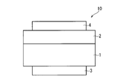
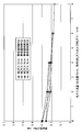
- FIG. 1 is a diagram schematically showing a configuration of a Schottky barrier diode 10.
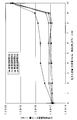
- FIG. It is the graph which plotted the value of Si concentration (Si impurity concentration) in various epitaxial substrates according to the flow volume of nitrogen gas in mixed gas atmosphere.
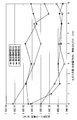
- 3 is a profile showing a result of SIMS measurement of an epitaxial substrate according to Example 1.
- FIG. 1 is a diagram showing a processing procedure for a group III nitride substrate according to the present embodiment.
- a group III nitride substrate is prepared (step S1).
- the group III nitride substrate is a free-standing substrate made of a group III nitride crystal (single crystal) represented by GaN, for example.
- the group III nitride substrate may be made of AlN, InN, BN, or the like in addition to GaN, or may be made of a mixed crystal thereof.
- substrate may be sufficient.
- it may be a so-called template substrate in which the group III nitride crystal layer described above is epitaxially formed on a substrate such as sapphire or silicon.
- the thickness of the group III nitride substrate is preferably about several hundred ⁇ m to several mm.
- a CMP (chemical mechanical polishing) process is performed on the prepared group III nitride substrate (step S2).
- CMP is preferably performed for about 2 to 5 hours using colloidal silica having a particle size of about 0.05 to 0.1 ⁇ m as abrasive grains.
- Rms root mean square roughness
- Rms is reduced to 0.1 nm to 0.3 nm by performing CMP.
- the In this embodiment, Rms is evaluated by measuring a 3 ⁇ m square region with an atomic force microscope (AFM) and analyzing the measurement result.
- AFM atomic force microscope
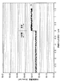
- FIG. 2 shows a result (profile) of SIMS (secondary ion mass spectrometry) measurement illustrating this.
- FIG. 2 shows the results of SIMS measurement in the case where a GaN layer exhibiting an n-type conductivity using Si as a dopant is formed immediately after the CMP process on the group III nitride substrate made of GaN by MOCVD. ing. Note that “depth from the interface” on the horizontal axis in FIG. 2 is the distance from the interface between the group III nitride substrate and the GaN layer in the stacking direction and the direction from the interface toward the group III nitride substrate. Is a value expressed with the direction toward the GaN layer being negative.
- FIG. 2 shows that Si impurities are unevenly distributed in the vicinity of the interface of the group III nitride substrate with the GaN layer at a concentration about 1 to 2 orders higher than the surroundings. In other words, it can be said that a Si impurity layer is formed. In addition, the present inventors confirmed that the presence of such Si impurities is a factor that degrades the characteristics of an electronic device fabricated by forming a group III nitride layer on a group III nitride substrate. Has been.
- the subsequent processing is performed on the group III nitride substrate for the purpose of removing Si impurities and making it possible to manufacture an electronic device having excellent characteristics.
- the group III nitride substrate subjected to CMP is heated and heated in a nitrogen gas atmosphere (step S3), and subsequently, a mixed atmosphere of hydrogen gas and nitrogen gas at a predetermined temperature, or hydrogen gas and A heat treatment (annealing treatment) is performed in a mixed atmosphere with ammonia gas (step S4).
- the temperature raising heating in the nitrogen gas atmosphere is performed until the substrate temperature reaches the temperature (annealing temperature) at which the subsequent annealing treatment is performed.
- the annealing temperature is preferably 950 ° C. or higher and 1150 ° C. or lower, and more preferably 1000 ° C. or higher and lower than 1100 ° C.
- the heating rate is preferably about 50 ° C./min to 120 ° C./min.
- the annealing treatment time is preferably about 4 to 8 minutes.
- the group III nitride in which the formation of the Si impurity layer on the surface is suitably suppressed A substrate is obtained.
- a group III nitride substrate By subjecting such a group III nitride substrate to a film forming process of a group III nitride layer for manufacturing an electronic device, it is possible to obtain an electronic device having excellent characteristics. For example, it is possible to obtain an electronic device with excellent withstand voltage characteristics in which a reverse leakage current that is a measure of withstand voltage in an electronic device is 1 ⁇ 10 ⁇ 5 A / cm 2 or less.
- the heating and annealing process is performed in a film forming apparatus that performs a process for forming a group III nitride layer on the group III nitride substrate.
- a CMP process is performed on the susceptor, which is a mounting position of the group III nitride substrate, when the group III nitride is formed in the reaction tube of the MOCVD apparatus.
- the subsequent group III nitride substrate is placed, and the group III nitride substrate is heated by heating the group III nitride substrate through a susceptor while flowing nitrogen gas from a nitrogen gas supply source in the reaction tube.
- Annealing treatment is performed by flowing at a flow rate ratio that satisfies the above-described mixing ratio. Then, after the annealing process is completed, a process for forming a group III nitride layer having a desired composition is performed.
- TMG trimethylgallium
- TMA trimethylaluminum
- TMI trimethylindium
- the group III nitride layer can be formed immediately on the clean group III nitride substrate after the annealing treatment, it is possible to fabricate an electronic device with more excellent characteristics.
- the heating and heating in the nitrogen gas atmosphere and the subsequent mixed atmosphere of hydrogen gas and nitrogen gas, or the hydrogen gas and ammonia gas By performing the annealing treatment in the mixed atmosphere, the formation of the Si impurity layer on the surface is suitably suppressed, and the characteristics are excellent when an electronic device is produced by epitaxially forming the group III nitride layer A group III nitride substrate from which an electronic device can be obtained can be obtained.
- Example 1 a plurality of group III nitride substrates were prepared, and after annealing treatment (heat treatment) in a mixed atmosphere of hydrogen gas and nitrogen gas while varying the processing conditions for each of them, An epitaxial substrate was fabricated using the group III nitride substrate after the annealing treatment.
- the epitaxial substrate refers to a group III nitride layer formed epitaxially on a group III nitride substrate.
- FIG. 3 is a diagram schematically showing the configuration of the Schottky barrier diode 10 manufactured in this example.
- a plurality of C-plane GaN free-standing substrates having a diameter of 4 inches, a thickness of 0.5 mm, and a Si doping amount of about 1 ⁇ 10 17 / cm 3 are prepared as a group III nitride substrate, Each was subjected to CMP treatment for 150 minutes.
- AFM measurement was performed for a 3 ⁇ m square range and Rms values were obtained, the Rms values of all the substrates were within the range of 0.15 nm to 0.20 nm.
- the group III nitride substrate after the CMP treatment is placed on the susceptor in the reaction tube of the MOCVD apparatus, and the group temperature of the group III nitride substrate is maintained in the nitrogen gas atmosphere while maintaining the pressure in the reaction tube at 0.3 atm (susceptor temperature). ) was increased to 1080 ° C.
- a mixed atmosphere of hydrogen gas and nitrogen gas at a predetermined mixing ratio was introduced into the reaction tube while maintaining the pressure in the reaction tube at 0.3 atm, and annealing treatment (heat treatment) was performed.
- the processing time was changed to four levels of 3 minutes, 4 minutes, 8 minutes, and 9 minutes.
- the flow rate of nitrogen gas is 0 slm (that is, only hydrogen gas atmosphere), 1 slm (only when the processing time is 8 minutes), 2 slm, 4 slm, 6 slm, 8 slm, 9 slm, while maintaining the total flow rate at 10 slm.
- the pressure in the reaction tube is set to 1 atm, hydrogen gas and nitrogen gas are used as carrier gas, ammonia gas and An n-type GaN layer was epitaxially formed to a thickness of 2 ⁇ m using TMG (trimethylgallium) bubbled with hydrogen gas as a source gas and silane gas as a dopant gas.
- TMG trimethylgallium
- the substrate temperature was lowered to room temperature, and the obtained epitaxial substrate was taken out from the MOCVD apparatus.
- Silane gas was introduced so that the Si concentration in the GaN layer was about 3 ⁇ 10 16 / cm 3 .
- the 3 ⁇ m square range of the surface of each of the obtained epitaxial substrates was measured with AFM, and Rms was calculated based on the obtained measurement results.
- each epitaxial substrate was cut out, and the Si concentration at the interface between the group III nitride substrate and the GaN layer was subjected to SIMS analysis, and the maximum value (peak value) in the obtained profile was obtained.
- the maximum value of the profile was obtained in the vicinity of the interface between the group III nitride substrate and the GaN layer.
- the Schottky barrier diode 10 shown in FIG. 3 was fabricated using the remaining part of the epitaxial substrate that was not subjected to SIMS analysis.
- the Schottky barrier diode 10 includes a base substrate 1, a GaN layer 2, an ohmic electrode 3 that is a multilayer electrode of Ti and Al, and a Schottky electrode 4 made of Ni.
- a metal mask with an opening diameter of 250 ⁇ m is placed so as to contact the surface of the base substrate 1 where the GaN layer 2 is not formed, and the Ti film and the Al film are EB (electron) so that their thicknesses become 30 nm and 1000 nm, respectively.
- the ohmic electrode 3 was obtained by vapor deposition. After vapor deposition, annealing was performed at 650 ° C. for 1 minute in a rapid annealing furnace (RTA).
- RTA rapid annealing furnace
- a Schottky electrode 4 was obtained by forming a Ni film with a thickness of 100 nm on the GaN layer 2 by EB vapor deposition using the same metal mask.
- the Schottky electrode 4 is formed at the same position as the ohmic electrode 3 in the thickness direction.
- the reverse leakage current was measured by applying a voltage in the range of 0 V to 600 V in the reverse direction to the Schottky barrier diode 10 obtained in the above manner.
- the maximum value of the Si impurity concentration is the Si group in the original group III nitride substrate. It remained at about 1 ⁇ 10 17 / cm 3 which is the same as the dope amount.
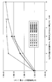
- FIG. 10 shows the result of SIMS measurement of an epitaxial substrate derived from a group III nitride substrate that has been annealed under conditions of an annealing time of 8 minutes and a nitrogen gas flow rate of 9 slm (hydrogen gas flow rate of 1 slm).
- Profile The “depth from the interface” on the horizontal axis in FIG. 10 is the same as in FIG.
- the Si concentration on the substrate side is approximately constant at about 1 ⁇ 10 17 / cm 3
- the GaN layer side The Si concentration is about 3 ⁇ 10 16 / cm 3 and is almost constant.
- the same profile is obtained for an epitaxial substrate fabricated using a group III nitride substrate that has been annealed under conditions where the annealing time is 4 minutes or more and the flow rate of nitrogen gas is 9 slm or less. Has been obtained.
- the group III nitride substrate and the GaN This means that the uneven distribution of Si impurities at the interface with the layer is suppressed.
- the surface roughness tends to deteriorate as the flow rate of nitrogen gas is lower and the annealing time is longer.
- the heat treatment time is 4 minutes and 8 minutes and the nitrogen gas flow rate is 2 slm or more (10 slm or less)
- the reverse leakage current is reduced to 1 ⁇ 10 ⁇ 5 A / cm 2 or less.
- nitrogen gas 8: 2 to 1: 9 with respect to the group III nitride substrate subjected to the CMP process.
- An annealing treatment of 8 minutes or less is suitable for manufacturing an electronic device using a group III nitride substrate having excellent characteristics by reducing the Si impurity concentration in the vicinity of the interface with the group III nitride GaN layer. It can be said that there is.
- the Si impurity concentration is reduced when the flow rate of nitrogen gas is lower than 2 slm (the mixing ratio of nitrogen gas is low and the mixing ratio of hydrogen gas is high).
- the surface roughness has deteriorated. Thereby, it is presumed that the interface between the Schottky electrode 4 and the GaN layer 2 is not well formed and the Schottky characteristics are deteriorated, and as a result, the reverse leakage current tends to increase. .
- Example 2 Except for changing the kind of mixed gas and the processing time in the annealing process, the same processes as in Example 1 were performed from the CMP process of the group III nitride substrate to the measurement of the reverse leakage current of the Schottky barrier diode.
- the processing time was set at 4 minutes and 2/8 levels.
- the flow rate of ammonia gas was fixed at 2 slm or 4 slm, the flow rate of nitrogen gas was variously different and the maximum was 8 slm, and the remainder was hydrogen gas.
- a mixed gas atmosphere of hydrogen gas and nitrogen gas instead of a mixed gas atmosphere of hydrogen gas and nitrogen gas, a mixed gas atmosphere of hydrogen gas and ammonia gas in which the mixing ratio of hydrogen gas to the whole mixed gas is 1/10 to 8/10 is used. Even in the case of annealing the group III nitride substrate after the CMP process, the Si impurity concentration is reduced in the vicinity of the interface between the group III nitride substrate and the GaN layer, and the group III nitride substrate is used. It indicates that an electronic device with excellent characteristics can be manufactured.
Landscapes
- Chemical & Material Sciences (AREA)
- Metallurgy (AREA)
- Engineering & Computer Science (AREA)
- Crystallography & Structural Chemistry (AREA)
- Materials Engineering (AREA)
- Organic Chemistry (AREA)
- General Chemical & Material Sciences (AREA)
- Chemical Kinetics & Catalysis (AREA)
- Inorganic Chemistry (AREA)
- Recrystallisation Techniques (AREA)
- Electrodes Of Semiconductors (AREA)
- Finish Polishing, Edge Sharpening, And Grinding By Specific Grinding Devices (AREA)
- Crystals, And After-Treatments Of Crystals (AREA)
- Mechanical Treatment Of Semiconductor (AREA)
Abstract
Description
本実施例では、複数のIII族窒化物基板を用意し、それぞれに対して処理条件を種々に違えつつ、水素ガスと窒素ガスとの混合雰囲気中でアニール処理(熱処理)を行った後、係るアニール処理後のIII族窒化物基板を用いたエピタキシャル基板の作製を行った。なお、本実施の形態において、エピタキシャル基板とは、III族窒化物基板上にIII族窒化物層をエピタキシャル形成したものを指し示すものとする。
アニール処理の際の混合ガスの種類と処理時間とを違えた他は、実施例1と同様に、III族窒化物基板のCMP処理からショットキーバリアダイオードの逆方向リーク電流測定までを行った。
Claims (7)
- III族窒化物基板の処理方法であって、
III族窒化物基板の表面を化学機械研磨処理するCMP工程と、
前記CMP工程を経た前記III族窒化物基板を窒素ガス雰囲気下で950℃以上1150℃以下のアニール温度にまで昇温する昇温工程と、
前記昇温工程によって前記アニール温度に昇温された前記III族窒化物基板を、水素ガスと窒素ガスとの第1の混合雰囲気または水素ガスとアンモニアガスとの第2の混合雰囲気中で4分以上8分以下保持するアニール工程と、
を備えることを特徴とするIII族窒化物基板の処理方法。 - 請求項1に記載のIII族窒化物基板の処理方法であって、
前記第1および第2の混合雰囲気における水素ガスの混合比を1/10~8/10とする、
ことを特徴とするIII族窒化物基板の処理方法。 - 請求項1または請求項2に記載のIII族窒化物基板の処理方法であって、
前記アニール温度を1000℃以上1100℃未満とする、
ことを特徴とするIII族窒化物基板の処理方法。 - III族窒化物基板上にIII族窒化物層がエピタキシャル形成されてなるエピタキシャル基板の製造方法であって、
III族窒化物基板の表面を化学機械研磨処理するCMP工程と、
前記CMP工程を経た前記III族窒化物基板を、前記III族窒化物基板上にIII族窒化物層をエピタキシャル形成するための装置内に載置する載置工程と、
前記載置工程を経た前記III族窒化物基板を前記装置内において窒素ガス雰囲気下で950℃以上1150℃以下のアニール温度にまで昇温する昇温工程と、
前記昇温工程によって前記アニール温度に昇温された前記III族窒化物基板を、前記装置内で水素ガスと窒素ガスとの第1の混合雰囲気または水素ガスとアンモニアガスとの第2の混合雰囲気中で4分以上8分以下保持するアニール工程と、
前記アニール工程を経た前記III族窒化物基板の上に前記装置内において前記III族窒化物層をエピタキシャル形成するエピタキシャル形成工程と、
を備えることを特徴とするエピタキシャル基板の製造方法。 - 請求項4に記載のエピタキシャル基板の製造方法であって、
前記第1および第2の混合雰囲気における水素ガスの混合比を1/10~8/10とする、
ことを特徴とするエピタキシャル基板の製造方法。 - 請求項4または請求項5に記載のエピタキシャル基板の製造方法であって、
前記アニール温度を1000℃以上1100℃未満とする、
ことを特徴とするエピタキシャル基板の製造方法。 - 請求項4ないし請求項6のいずれかに記載のエピタキシャル基板の製造方法であって、
前記エピタキシャル工程における前記III族窒化物層のエピタキシャル形成温度を前記アニール温度と同じにする、
ことを特徴とするエピタキシャル基板の製造方法。
Priority Applications (5)
| Application Number | Priority Date | Filing Date | Title |
|---|---|---|---|
| CN201480000946.6A CN104246987B (zh) | 2013-03-29 | 2014-03-20 | Iii族氮化物基板的处理方法及外延基板的制造方法 |
| JP2014544847A JP6019129B2 (ja) | 2013-03-29 | 2014-03-20 | Iii族窒化物基板の処理方法およびエピタキシャル基板の製造方法 |
| KR1020147027736A KR102100841B1 (ko) | 2013-03-29 | 2014-03-20 | Iii족 질화물 기판의 처리 방법 및 에피택셜 기판의 제조 방법 |
| EP14772262.3A EP2821532B1 (en) | 2013-03-29 | 2014-03-20 | Method for treating a group-iii nitride substrate and method for manufacturing an epitaxial substrate |
| US14/499,336 US9196480B2 (en) | 2013-03-29 | 2014-09-29 | Method for treating group III nitride substrate and method for manufacturing epitaxial substrate |
Applications Claiming Priority (2)
| Application Number | Priority Date | Filing Date | Title |
|---|---|---|---|
| JP2013072508 | 2013-03-29 | ||
| JP2013-072508 | 2013-03-29 |
Related Child Applications (1)
| Application Number | Title | Priority Date | Filing Date |
|---|---|---|---|
| US14/499,336 Continuation US9196480B2 (en) | 2013-03-29 | 2014-09-29 | Method for treating group III nitride substrate and method for manufacturing epitaxial substrate |
Publications (1)
| Publication Number | Publication Date |
|---|---|
| WO2014156914A1 true WO2014156914A1 (ja) | 2014-10-02 |
Family
ID=51623893
Family Applications (1)
| Application Number | Title | Priority Date | Filing Date |
|---|---|---|---|
| PCT/JP2014/057649 Ceased WO2014156914A1 (ja) | 2013-03-29 | 2014-03-20 | Iii族窒化物基板の処理方法およびエピタキシャル基板の製造方法 |
Country Status (7)
| Country | Link |
|---|---|
| US (1) | US9196480B2 (ja) |
| EP (1) | EP2821532B1 (ja) |
| JP (1) | JP6019129B2 (ja) |
| KR (1) | KR102100841B1 (ja) |
| CN (1) | CN104246987B (ja) |
| TW (1) | TWI600076B (ja) |
| WO (1) | WO2014156914A1 (ja) |
Cited By (2)
| Publication number | Priority date | Publication date | Assignee | Title |
|---|---|---|---|---|
| JP2019026526A (ja) * | 2017-08-01 | 2019-02-21 | 株式会社サイオクス | 半導体積層物の製造方法、窒化物半導体自立基板の製造方法、半導体積層物および半導体装置 |
| WO2022079939A1 (ja) * | 2020-10-14 | 2022-04-21 | 日本碍子株式会社 | Iii族元素窒化物半導体基板 |
Families Citing this family (5)
| Publication number | Priority date | Publication date | Assignee | Title |
|---|---|---|---|---|
| JP7055595B2 (ja) * | 2017-03-29 | 2022-04-18 | 古河機械金属株式会社 | Iii族窒化物半導体基板、及び、iii族窒化物半導体基板の製造方法 |
| CN114420753B (zh) * | 2020-10-28 | 2025-09-02 | 江苏第三代半导体研究院有限公司 | HEMT器件、基于GaN衬底的HEMT外延结构及制作方法 |
| CN113053731B (zh) * | 2021-03-05 | 2024-05-17 | 中国科学院苏州纳米技术与纳米仿生研究所 | 镓金属薄膜的制作方法以及氮化镓衬底的保护方法 |
| WO2023123567A1 (zh) * | 2021-12-28 | 2023-07-06 | 江苏第三代半导体研究院有限公司 | 半导体加工系统及半导体加工方法 |
| CN114664642B (zh) * | 2022-03-23 | 2023-07-04 | 江苏第三代半导体研究院有限公司 | 基于iii族氮化物同质外延的hemt结构、其制备方法及应用 |
Citations (7)
| Publication number | Priority date | Publication date | Assignee | Title |
|---|---|---|---|---|
| JP2001322899A (ja) * | 2000-05-11 | 2001-11-20 | Matsushita Electric Ind Co Ltd | 窒化ガリウム系化合物半導体基板及びその製造方法 |
| JP3631724B2 (ja) | 2001-03-27 | 2005-03-23 | 日本電気株式会社 | Iii族窒化物半導体基板およびその製造方法 |
| JP2005136311A (ja) * | 2003-10-31 | 2005-05-26 | Matsushita Electric Ind Co Ltd | 窒化物半導体基板及びその製造方法 |
| JP3894191B2 (ja) | 2003-11-26 | 2007-03-14 | 住友電気工業株式会社 | 窒化ガリウム系半導体膜を形成する方法、および半導体基板生産物 |
| JP2010163307A (ja) * | 2009-01-14 | 2010-07-29 | Sumitomo Electric Ind Ltd | Iii族窒化物基板、それを備える半導体デバイス、及び、表面処理されたiii族窒化物基板を製造する方法 |
| JP4984557B2 (ja) | 2005-03-04 | 2012-07-25 | 住友電気工業株式会社 | 縦型窒化ガリウム半導体装置を作製する方法、エピタキシャル基板を作製する方法 |
| JP2012235136A (ja) * | 2001-06-08 | 2012-11-29 | Cree Inc | ウェーハ、エピタキシャルAlxGayInzN結晶構造体、エピタキシャルAlx’Gay’Inz’N結晶ブール、光電子デバイスおよびマイクロ電子デバイス |
Family Cites Families (10)
| Publication number | Priority date | Publication date | Assignee | Title |
|---|---|---|---|---|
| NL7900244A (nl) | 1979-01-12 | 1980-07-15 | Philips Nv | Vlakke tweelaags electrische spoel. |
| JP3658756B2 (ja) * | 1999-03-01 | 2005-06-08 | 住友電気工業株式会社 | 化合物半導体の製造方法 |
| JP2003327497A (ja) * | 2002-05-13 | 2003-11-19 | Sumitomo Electric Ind Ltd | GaN単結晶基板、窒化物系半導体エピタキシャル基板、窒化物系半導体素子及びその製造方法 |
| JP2004035360A (ja) * | 2002-07-05 | 2004-02-05 | Sumitomo Electric Ind Ltd | GaN単結晶基板、窒化物系半導体エピタキシャル基板及びその製造方法 |
| US7045808B2 (en) | 2003-12-26 | 2006-05-16 | Hitachi Cable, Ltd. | III-V nitride semiconductor substrate and its production lot, and III-V nitride semiconductor device and its production method |
| CA2563731A1 (en) | 2005-03-04 | 2006-09-08 | Sumitomo Electric Industries, Ltd. | Vertical gallium nitride semiconductor device and epitaxial substrate |
| JP5108641B2 (ja) * | 2008-06-12 | 2012-12-26 | 住友電気工業株式会社 | GaN単結晶基板、窒化物系半導体エピタキシャル基板、及び、窒化物系半導体素子 |
| JP2010084675A (ja) | 2008-10-01 | 2010-04-15 | Denso Corp | 内燃機関の異常検出装置 |
| CN102282299B (zh) | 2009-01-21 | 2014-07-02 | 日本碍子株式会社 | 13族氮化物晶板 |
| JP4513927B1 (ja) * | 2009-09-30 | 2010-07-28 | 住友電気工業株式会社 | Iii族窒化物半導体基板、エピタキシャル基板及び半導体デバイス |
-
2014
- 2014-03-20 KR KR1020147027736A patent/KR102100841B1/ko active Active
- 2014-03-20 WO PCT/JP2014/057649 patent/WO2014156914A1/ja not_active Ceased
- 2014-03-20 JP JP2014544847A patent/JP6019129B2/ja active Active
- 2014-03-20 EP EP14772262.3A patent/EP2821532B1/en active Active
- 2014-03-20 CN CN201480000946.6A patent/CN104246987B/zh active Active
- 2014-03-24 TW TW103110835A patent/TWI600076B/zh active
- 2014-09-29 US US14/499,336 patent/US9196480B2/en active Active
Patent Citations (7)
| Publication number | Priority date | Publication date | Assignee | Title |
|---|---|---|---|---|
| JP2001322899A (ja) * | 2000-05-11 | 2001-11-20 | Matsushita Electric Ind Co Ltd | 窒化ガリウム系化合物半導体基板及びその製造方法 |
| JP3631724B2 (ja) | 2001-03-27 | 2005-03-23 | 日本電気株式会社 | Iii族窒化物半導体基板およびその製造方法 |
| JP2012235136A (ja) * | 2001-06-08 | 2012-11-29 | Cree Inc | ウェーハ、エピタキシャルAlxGayInzN結晶構造体、エピタキシャルAlx’Gay’Inz’N結晶ブール、光電子デバイスおよびマイクロ電子デバイス |
| JP2005136311A (ja) * | 2003-10-31 | 2005-05-26 | Matsushita Electric Ind Co Ltd | 窒化物半導体基板及びその製造方法 |
| JP3894191B2 (ja) | 2003-11-26 | 2007-03-14 | 住友電気工業株式会社 | 窒化ガリウム系半導体膜を形成する方法、および半導体基板生産物 |
| JP4984557B2 (ja) | 2005-03-04 | 2012-07-25 | 住友電気工業株式会社 | 縦型窒化ガリウム半導体装置を作製する方法、エピタキシャル基板を作製する方法 |
| JP2010163307A (ja) * | 2009-01-14 | 2010-07-29 | Sumitomo Electric Ind Ltd | Iii族窒化物基板、それを備える半導体デバイス、及び、表面処理されたiii族窒化物基板を製造する方法 |
Non-Patent Citations (1)
| Title |
|---|
| See also references of EP2821532A4 |
Cited By (3)
| Publication number | Priority date | Publication date | Assignee | Title |
|---|---|---|---|---|
| JP2019026526A (ja) * | 2017-08-01 | 2019-02-21 | 株式会社サイオクス | 半導体積層物の製造方法、窒化物半導体自立基板の製造方法、半導体積層物および半導体装置 |
| WO2022079939A1 (ja) * | 2020-10-14 | 2022-04-21 | 日本碍子株式会社 | Iii族元素窒化物半導体基板 |
| US12057307B2 (en) | 2020-10-14 | 2024-08-06 | Ngk Insulators, Ltd. | Group-III element nitride semiconductor substrate |
Also Published As
| Publication number | Publication date |
|---|---|
| TW201511109A (zh) | 2015-03-16 |
| EP2821532A4 (en) | 2015-10-07 |
| US9196480B2 (en) | 2015-11-24 |
| CN104246987B (zh) | 2017-10-13 |
| EP2821532A1 (en) | 2015-01-07 |
| JPWO2014156914A1 (ja) | 2017-02-16 |
| JP6019129B2 (ja) | 2016-11-02 |
| KR20150140202A (ko) | 2015-12-15 |
| US20150017786A1 (en) | 2015-01-15 |
| CN104246987A (zh) | 2014-12-24 |
| KR102100841B1 (ko) | 2020-04-14 |
| TWI600076B (zh) | 2017-09-21 |
| EP2821532B1 (en) | 2018-01-10 |
Similar Documents
| Publication | Publication Date | Title |
|---|---|---|
| CN108140563B (zh) | 半导体元件用外延基板、半导体元件和半导体元件用外延基板的制造方法 | |
| JP6019129B2 (ja) | Iii族窒化物基板の処理方法およびエピタキシャル基板の製造方法 | |
| CN105658848A (zh) | n型氮化铝单晶基板以及垂直型氮化物半导体器件 | |
| TWI699462B (zh) | Iii族氮化物半導體基板的製造方法 | |
| WO2017077989A1 (ja) | 半導体素子用エピタキシャル基板、半導体素子、および、半導体素子用エピタキシャル基板の製造方法 | |
| JP2004111848A (ja) | サファイア基板とそれを用いたエピタキシャル基板およびその製造方法 | |
| CN108352327B (zh) | 半导体元件用外延基板、半导体元件和半导体元件用外延基板的制造方法 | |
| JP5378128B2 (ja) | 電子デバイス用エピタキシャル基板およびiii族窒化物電子デバイス用エピタキシャル基板 | |
| JP5537890B2 (ja) | 酸化亜鉛系半導体発光素子の製造方法 | |
| JP2016533643A (ja) | 半導体ウェハおよび半導体ウェハを製造するための方法 | |
| JP5614130B2 (ja) | 半導体装置の製造方法 |
Legal Events
| Date | Code | Title | Description |
|---|---|---|---|
| ENP | Entry into the national phase |
Ref document number: 2014544847 Country of ref document: JP Kind code of ref document: A |
|
| ENP | Entry into the national phase |
Ref document number: 20147027736 Country of ref document: KR Kind code of ref document: A |
|
| WWE | Wipo information: entry into national phase |
Ref document number: 2014772262 Country of ref document: EP |
|
| 121 | Ep: the epo has been informed by wipo that ep was designated in this application |
Ref document number: 14772262 Country of ref document: EP Kind code of ref document: A1 |
|
| NENP | Non-entry into the national phase |
Ref country code: DE |