WO2014167625A1 - Dispositif de conversion d'énergie, dispositif motorisé comprenant le même dispositif, ventilateur comprenant le même dispositif, compresseur, et climatiseur, réfrigérateur, et congélateur comprenant les mêmes dispositifs - Google Patents
Dispositif de conversion d'énergie, dispositif motorisé comprenant le même dispositif, ventilateur comprenant le même dispositif, compresseur, et climatiseur, réfrigérateur, et congélateur comprenant les mêmes dispositifs Download PDFInfo
- Publication number
- WO2014167625A1 WO2014167625A1 PCT/JP2013/060619 JP2013060619W WO2014167625A1 WO 2014167625 A1 WO2014167625 A1 WO 2014167625A1 JP 2013060619 W JP2013060619 W JP 2013060619W WO 2014167625 A1 WO2014167625 A1 WO 2014167625A1
- Authority
- WO
- WIPO (PCT)
- Prior art keywords
- overcurrent detection
- phase
- lower arm
- detection result
- power supply
- Prior art date
- Legal status (The legal status is an assumption and is not a legal conclusion. Google has not performed a legal analysis and makes no representation as to the accuracy of the status listed.)
- Ceased
Links
Images






Classifications
-
- H—ELECTRICITY
- H02—GENERATION; CONVERSION OR DISTRIBUTION OF ELECTRIC POWER
- H02P—CONTROL OR REGULATION OF ELECTRIC MOTORS, ELECTRIC GENERATORS OR DYNAMO-ELECTRIC CONVERTERS; CONTROLLING TRANSFORMERS, REACTORS OR CHOKE COILS
- H02P29/00—Arrangements for regulating or controlling electric motors, appropriate for both AC and DC motors
- H02P29/02—Providing protection against overload without automatic interruption of supply
- H02P29/024—Detecting a fault condition, e.g. short circuit, locked rotor, open circuit or loss of load
- H02P29/027—Detecting a fault condition, e.g. short circuit, locked rotor, open circuit or loss of load the fault being an over-current
-
- F—MECHANICAL ENGINEERING; LIGHTING; HEATING; WEAPONS; BLASTING
- F04—POSITIVE - DISPLACEMENT MACHINES FOR LIQUIDS; PUMPS FOR LIQUIDS OR ELASTIC FLUIDS
- F04D—NON-POSITIVE-DISPLACEMENT PUMPS
- F04D25/00—Pumping installations or systems
- F04D25/02—Units comprising pumps and their driving means
- F04D25/06—Units comprising pumps and their driving means the pump being electrically driven
-
- F—MECHANICAL ENGINEERING; LIGHTING; HEATING; WEAPONS; BLASTING
- F04—POSITIVE - DISPLACEMENT MACHINES FOR LIQUIDS; PUMPS FOR LIQUIDS OR ELASTIC FLUIDS
- F04D—NON-POSITIVE-DISPLACEMENT PUMPS
- F04D25/00—Pumping installations or systems
- F04D25/02—Units comprising pumps and their driving means
- F04D25/08—Units comprising pumps and their driving means the working fluid being air, e.g. for ventilation
-
- F—MECHANICAL ENGINEERING; LIGHTING; HEATING; WEAPONS; BLASTING
- F25—REFRIGERATION OR COOLING; COMBINED HEATING AND REFRIGERATION SYSTEMS; HEAT PUMP SYSTEMS; MANUFACTURE OR STORAGE OF ICE; LIQUEFACTION SOLIDIFICATION OF GASES
- F25B—REFRIGERATION MACHINES, PLANTS OR SYSTEMS; COMBINED HEATING AND REFRIGERATION SYSTEMS; HEAT PUMP SYSTEMS
- F25B31/00—Compressor arrangements
- F25B31/02—Compressor arrangements of motor-compressor units
-
- H—ELECTRICITY
- H02—GENERATION; CONVERSION OR DISTRIBUTION OF ELECTRIC POWER
- H02H—EMERGENCY PROTECTIVE CIRCUIT ARRANGEMENTS
- H02H7/00—Emergency protective circuit arrangements specially adapted for specific types of electric machines or apparatus or for sectionalised protection of cable or line systems, and effecting automatic switching in the event of an undesired change from normal working conditions
- H02H7/10—Emergency protective circuit arrangements specially adapted for specific types of electric machines or apparatus or for sectionalised protection of cable or line systems, and effecting automatic switching in the event of an undesired change from normal working conditions for converters; for rectifiers
-
- H—ELECTRICITY
- H02—GENERATION; CONVERSION OR DISTRIBUTION OF ELECTRIC POWER
- H02M—APPARATUS FOR CONVERSION BETWEEN AC AND AC, BETWEEN AC AND DC, OR BETWEEN DC AND DC, AND FOR USE WITH MAINS OR SIMILAR POWER SUPPLY SYSTEMS; CONVERSION OF DC OR AC INPUT POWER INTO SURGE OUTPUT POWER; CONTROL OR REGULATION THEREOF
- H02M1/00—Details of apparatus for conversion
- H02M1/32—Means for protecting converters other than automatic disconnection
-
- H—ELECTRICITY
- H02—GENERATION; CONVERSION OR DISTRIBUTION OF ELECTRIC POWER
- H02M—APPARATUS FOR CONVERSION BETWEEN AC AND AC, BETWEEN AC AND DC, OR BETWEEN DC AND DC, AND FOR USE WITH MAINS OR SIMILAR POWER SUPPLY SYSTEMS; CONVERSION OF DC OR AC INPUT POWER INTO SURGE OUTPUT POWER; CONTROL OR REGULATION THEREOF
- H02M7/00—Conversion of AC power input into DC power output; Conversion of DC power input into AC power output
- H02M7/42—Conversion of DC power input into AC power output without possibility of reversal
- H02M7/44—Conversion of DC power input into AC power output without possibility of reversal by static converters
- H02M7/48—Conversion of DC power input into AC power output without possibility of reversal by static converters using discharge tubes with control electrode or semiconductor devices with control electrode
- H02M7/53—Conversion of DC power input into AC power output without possibility of reversal by static converters using discharge tubes with control electrode or semiconductor devices with control electrode using devices of a triode or transistor type requiring continuous application of a control signal
- H02M7/537—Conversion of DC power input into AC power output without possibility of reversal by static converters using discharge tubes with control electrode or semiconductor devices with control electrode using devices of a triode or transistor type requiring continuous application of a control signal using semiconductor devices only, e.g. single switched pulse inverters
-
- H—ELECTRICITY
- H02—GENERATION; CONVERSION OR DISTRIBUTION OF ELECTRIC POWER
- H02M—APPARATUS FOR CONVERSION BETWEEN AC AND AC, BETWEEN AC AND DC, OR BETWEEN DC AND DC, AND FOR USE WITH MAINS OR SIMILAR POWER SUPPLY SYSTEMS; CONVERSION OF DC OR AC INPUT POWER INTO SURGE OUTPUT POWER; CONTROL OR REGULATION THEREOF
- H02M7/00—Conversion of AC power input into DC power output; Conversion of DC power input into AC power output
- H02M7/42—Conversion of DC power input into AC power output without possibility of reversal
- H02M7/44—Conversion of DC power input into AC power output without possibility of reversal by static converters
- H02M7/48—Conversion of DC power input into AC power output without possibility of reversal by static converters using discharge tubes with control electrode or semiconductor devices with control electrode
- H02M7/53—Conversion of DC power input into AC power output without possibility of reversal by static converters using discharge tubes with control electrode or semiconductor devices with control electrode using devices of a triode or transistor type requiring continuous application of a control signal
- H02M7/537—Conversion of DC power input into AC power output without possibility of reversal by static converters using discharge tubes with control electrode or semiconductor devices with control electrode using devices of a triode or transistor type requiring continuous application of a control signal using semiconductor devices only, e.g. single switched pulse inverters
- H02M7/5387—Conversion of DC power input into AC power output without possibility of reversal by static converters using discharge tubes with control electrode or semiconductor devices with control electrode using devices of a triode or transistor type requiring continuous application of a control signal using semiconductor devices only, e.g. single switched pulse inverters in a bridge configuration
- H02M7/53871—Conversion of DC power input into AC power output without possibility of reversal by static converters using discharge tubes with control electrode or semiconductor devices with control electrode using devices of a triode or transistor type requiring continuous application of a control signal using semiconductor devices only, e.g. single switched pulse inverters in a bridge configuration with automatic control of output voltage or current
-
- H—ELECTRICITY
- H02—GENERATION; CONVERSION OR DISTRIBUTION OF ELECTRIC POWER
- H02P—CONTROL OR REGULATION OF ELECTRIC MOTORS, ELECTRIC GENERATORS OR DYNAMO-ELECTRIC CONVERTERS; CONTROLLING TRANSFORMERS, REACTORS OR CHOKE COILS
- H02P27/00—Arrangements or methods for the control of AC motors characterised by the kind of supply voltage
- H02P27/04—Arrangements or methods for the control of AC motors characterised by the kind of supply voltage using variable-frequency supply voltage, e.g. inverter or converter supply voltage
- H02P27/06—Arrangements or methods for the control of AC motors characterised by the kind of supply voltage using variable-frequency supply voltage, e.g. inverter or converter supply voltage using DC to AC converters or inverters
-
- F—MECHANICAL ENGINEERING; LIGHTING; HEATING; WEAPONS; BLASTING
- F25—REFRIGERATION OR COOLING; COMBINED HEATING AND REFRIGERATION SYSTEMS; HEAT PUMP SYSTEMS; MANUFACTURE OR STORAGE OF ICE; LIQUEFACTION SOLIDIFICATION OF GASES
- F25B—REFRIGERATION MACHINES, PLANTS OR SYSTEMS; COMBINED HEATING AND REFRIGERATION SYSTEMS; HEAT PUMP SYSTEMS
- F25B2600/00—Control issues
- F25B2600/02—Compressor control
- F25B2600/021—Inverters therefor
-
- F—MECHANICAL ENGINEERING; LIGHTING; HEATING; WEAPONS; BLASTING
- F25—REFRIGERATION OR COOLING; COMBINED HEATING AND REFRIGERATION SYSTEMS; HEAT PUMP SYSTEMS; MANUFACTURE OR STORAGE OF ICE; LIQUEFACTION SOLIDIFICATION OF GASES
- F25B—REFRIGERATION MACHINES, PLANTS OR SYSTEMS; COMBINED HEATING AND REFRIGERATION SYSTEMS; HEAT PUMP SYSTEMS
- F25B49/00—Arrangement or mounting of control or safety devices
- F25B49/02—Arrangement or mounting of control or safety devices for compression type machines, plants or systems
- F25B49/025—Motor control arrangements
-
- H—ELECTRICITY
- H02—GENERATION; CONVERSION OR DISTRIBUTION OF ELECTRIC POWER
- H02H—EMERGENCY PROTECTIVE CIRCUIT ARRANGEMENTS
- H02H3/00—Emergency protective circuit arrangements for automatic disconnection directly responsive to an undesired change from normal electric working condition with or without subsequent reconnection ; integrated protection
- H02H3/08—Emergency protective circuit arrangements for automatic disconnection directly responsive to an undesired change from normal electric working condition with or without subsequent reconnection ; integrated protection responsive to excess current
-
- H—ELECTRICITY
- H02—GENERATION; CONVERSION OR DISTRIBUTION OF ELECTRIC POWER
- H02H—EMERGENCY PROTECTIVE CIRCUIT ARRANGEMENTS
- H02H7/00—Emergency protective circuit arrangements specially adapted for specific types of electric machines or apparatus or for sectionalised protection of cable or line systems, and effecting automatic switching in the event of an undesired change from normal working conditions
- H02H7/10—Emergency protective circuit arrangements specially adapted for specific types of electric machines or apparatus or for sectionalised protection of cable or line systems, and effecting automatic switching in the event of an undesired change from normal working conditions for converters; for rectifiers
- H02H7/12—Emergency protective circuit arrangements specially adapted for specific types of electric machines or apparatus or for sectionalised protection of cable or line systems, and effecting automatic switching in the event of an undesired change from normal working conditions for converters; for rectifiers for static converters or rectifiers
- H02H7/122—Emergency protective circuit arrangements specially adapted for specific types of electric machines or apparatus or for sectionalised protection of cable or line systems, and effecting automatic switching in the event of an undesired change from normal working conditions for converters; for rectifiers for static converters or rectifiers for inverters, i.e. DC/AC converters
- H02H7/1227—Emergency protective circuit arrangements specially adapted for specific types of electric machines or apparatus or for sectionalised protection of cable or line systems, and effecting automatic switching in the event of an undesired change from normal working conditions for converters; for rectifiers for static converters or rectifiers for inverters, i.e. DC/AC converters responsive to abnormalities in the output circuit, e.g. short circuit
-
- H—ELECTRICITY
- H02—GENERATION; CONVERSION OR DISTRIBUTION OF ELECTRIC POWER
- H02M—APPARATUS FOR CONVERSION BETWEEN AC AND AC, BETWEEN AC AND DC, OR BETWEEN DC AND DC, AND FOR USE WITH MAINS OR SIMILAR POWER SUPPLY SYSTEMS; CONVERSION OF DC OR AC INPUT POWER INTO SURGE OUTPUT POWER; CONTROL OR REGULATION THEREOF
- H02M1/00—Details of apparatus for conversion
- H02M1/0003—Details of control, feedback or regulation circuits
- H02M1/0009—Devices or circuits for detecting current in a converter
-
- Y—GENERAL TAGGING OF NEW TECHNOLOGICAL DEVELOPMENTS; GENERAL TAGGING OF CROSS-SECTIONAL TECHNOLOGIES SPANNING OVER SEVERAL SECTIONS OF THE IPC; TECHNICAL SUBJECTS COVERED BY FORMER USPC CROSS-REFERENCE ART COLLECTIONS [XRACs] AND DIGESTS
- Y02—TECHNOLOGIES OR APPLICATIONS FOR MITIGATION OR ADAPTATION AGAINST CLIMATE CHANGE
- Y02B—CLIMATE CHANGE MITIGATION TECHNOLOGIES RELATED TO BUILDINGS, e.g. HOUSING, HOUSE APPLIANCES OR RELATED END-USER APPLICATIONS
- Y02B30/00—Energy efficient heating, ventilation or air conditioning [HVAC]
- Y02B30/70—Efficient control or regulation technologies, e.g. for control of refrigerant flow, motor or heating
Definitions
- the present invention relates to a power conversion device, a motor driving device including the power conversion device, a blower and a compressor including the power conversion device, an air conditioner including the same, a refrigerator, and a refrigerator.
- a power conversion device that generates a three-phase AC voltage and supplies it to a load by combining ON / OFF states of switching elements constituting a PWM-modulated three-phase inverter, for example, each phase flowing through a three-phase load such as a motor The current is detected, and the load is controlled based on each phase current.
- a configuration in which a shunt resistor is provided includes a configuration in which a power supply shunt resistor that detects a current between the DC power supply and the inverter device is provided, or a phase current of the relevant phase that is detected between the lower arm switching element and the negative side of the DC power supply.
- a configuration in which an arm shunt resistor is provided In the configuration in which the power supply shunt resistor and the lower arm shunt resistor are provided, it is necessary to specify the phase current to be detected for each phase, which complicates the control software.
- the power supply shunt resistor when only the current for one phase can be detected, it is necessary to adjust the energization to detect the current for two phases. That is, the period for detecting each phase current in one switching cycle is limited to a narrow range. For this reason, for example, by providing a power supply shunt resistor and a lower arm shunt resistor for at least two phases and detecting a phase current that cannot be detected by the lower arm shunt resistor, the detected current for each phase
- An inverter device that can detect phase currents with simple control software that does not require identification, energization adjustment, and time-series current detection is disclosed (for example, Patent Document 1).
- the present invention has been made in view of the above, and realizes an extension of the overcurrent detection period of the phase current and simplification of the overcurrent detection procedure, thereby improving the operation reliability of the inverter and the load device.
- An object of the present invention is to provide a power conversion device that can be used.
- a power conversion device is a power conversion device that converts DC power supplied from a DC power source into three-phase AC power and supplies it to a load device.
- An inverter configured by connecting arms composed of an upper arm switching element and a lower arm switching element in parallel for three phases; a power shunt resistor provided between the negative voltage side of the DC power supply and the inverter; Each phase lower arm shunt resistor provided between each phase lower arm switching element and the power shunt resistor, a connection point between the power shunt resistor and each phase lower arm shunt resistor, and a negative voltage of the DC power source
- a first overcurrent detection for detecting an overcurrent of a current flowing through the power shunt resistor based on a power shunt resistor voltage which is a voltage between Each phase lower arm switching element and each phase lower arm shunt resistor, and each phase lower arm voltage based on each phase lower arm voltage which is each voltage between the negative voltage side of the DC
- the phase current overcurrent detection period can be extended and the overcurrent detection procedure can be simplified, and the operation reliability of the inverter and the load device can be improved.
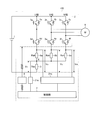
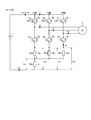
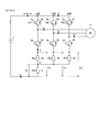
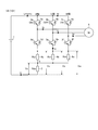
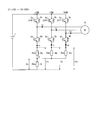
- FIG. 1 is a diagram of a configuration example of the power conversion apparatus according to the first embodiment.
- FIG. 2 is a diagram of a configuration example of the first overcurrent detection unit of the power conversion device according to the first embodiment.
- FIG. 3 is a diagram of a configuration example of the second overcurrent detection unit of the power conversion device according to the first embodiment.
- FIG. 4 is a diagram of a configuration example of a control unit of the power conversion device according to the first embodiment.
- FIG. 5 is a diagram showing the relationship between the ON / OFF state of each phase upper arm switching element and the output voltage vector of the inverter in the space vector modulation method.
- FIG. 6 is a diagram illustrating a current flowing through each part of the inverter when the output voltage vector of the inverter is a real vector V1 (100).
- FIG. 7 is a diagram illustrating currents that flow through each part of the inverter when the output voltage vector of the inverter is the real vector V2 (010).
- FIG. 8 is a diagram illustrating currents that flow through each part of the inverter when the output voltage vector of the inverter is the real vector V3 (001).
- FIG. 9 is a diagram illustrating currents that flow through each part of the inverter when the output voltage vector of the inverter is the zero vector V4 (110).
- FIG. 10 is a diagram illustrating currents that flow through each part of the inverter when the output voltage vector of the inverter is the real vector V5 (011).
- FIG. 11 is a diagram illustrating currents that flow through each part of the inverter when the output voltage vector of the inverter is the real vector V6 (101).
- FIG. 12 is a diagram illustrating currents that flow through each part of the inverter when the output voltage vector of the inverter is the real vector V0 (000).
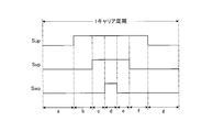
- FIG. 13 is a diagram illustrating an example of each output voltage vector generation period in one carrier cycle.
- FIG. 14 is a diagram showing the transition of the power supply shunt resistance voltage Vx when the modulation rate of the inverter is relatively high.
- FIG. 15 is a diagram showing the transition of the power supply shunt resistance voltage Vx when the modulation rate of the inverter is relatively low.
- FIG. 16 is a diagram showing a transition of the U-phase lower arm voltage Vu when the modulation rate of the inverter is relatively low.
- FIG. 1 is a diagram of a configuration example of the power conversion apparatus according to the first embodiment.
- the power conversion device 100 converts DC power supplied from the DC power source 1 into three-phase AC power supplied to a load device (a motor in the example illustrated in FIG. 1) 9. It is configured to do.
- the power conversion device 100 includes upper arm switching elements 3a to 3c (here, 3a: U phase, 3b: V) as main components for supplying three-phase AC power to the load device 9.
- lower arm switching elements 3d-3f (here, 3d: U phase, 3e: V phase, 3f: W phase) inverter 2 composed of three arms, and on each phase
- Six drive signals corresponding to the arm switching elements 3a to 3c and the lower arm switching elements 3d to 3f are generated and output to the upper arm switching elements 3a to 3c and the lower arm switching elements 3d to 3f, respectively.
- Each phase upper arm switching element 3a to 3c and each phase lower arm switching element 3d to 3f are respectively connected to anti-reflective diodes 4a to 4f (here, 4a: U-phase upper arm, 4b: V-phase upper arm, 4c: W-phase upper arm, 4d: U-phase lower arm, 4e: V-phase lower arm, 4f: W-phase lower arm).
- the control unit 7 is constituted by, for example, a microcomputer, a CPU, and the like, and is an arithmetic / control unit that converts an input analog voltage signal into a digital value and performs arithmetic / control in accordance with the control application of the load device 9.
- the power conversion device 100 includes a power shunt resistor 5 provided between the negative voltage side of the DC power source 1 and the inverter 2, lower-phase arm switching elements 3d, 3e, 3f, and a power source.
- Each phase lower arm shunt resistor 6a, 6b, 6c (here 6a: U phase, 6b: V phase, 6c: W phase) provided between each and shunt resistor 5, power supply shunt resistor 5 and each phase Vx between the connection point (point X shown in FIG.
- phase lower arm voltages Based on the voltages Vu, Vv, Vw between the connection point and the negative voltage side (reference potential) of the DC power source 1 (hereinafter referred to as “phase lower arm voltages”), the respective phase lower arm shunt resistors 6a, 6b.
- the resistance value of the power supply shunt resistor 5 is Rdc
- the resistance values of the lower arm shunt resistors 6a, 6b, and 6c are Rsh.
- FIG. 2 is a diagram of a configuration example of the first overcurrent detection unit of the power conversion device according to the first embodiment. As shown in FIG. 2, the first overcurrent detection unit 21 a includes a voltage comparison unit 22.
- the power supply shunt resistance 5 is set.
- a value (here, Hi output) indicating that the current value of the flowing current is a normal value is output to the control unit 7 as an OC1 output, and the power supply shunt resistance voltage Vx is larger than the first threshold value V1 (Vx> V1). )
- a value indicating that an overcurrent has flowed through the power supply shunt resistor 5 (here, Lo output) is output to the control unit 7 as an OC1 output.
- the first overcurrent detection unit 21a includes an amplifying unit for setting the power supply shunt resistance voltage Vx to a voltage value Vx ′ that can be easily handled by the control unit 7 before the voltage comparison unit 22. Also good. In this case, in the voltage comparison unit 22, when Vx ′ is equal to or lower than a preset first threshold value V1 ′ (Vx ′ ⁇ V1 ′), the current value of the current flowing through the power supply shunt resistor 5 is normal.
- the power supply shunt A value indicating that an overcurrent has flowed through the resistor 5 (here, Lo output) may be output to the control unit 7 as the OC1 output.
- FIG. 3 is a diagram of a configuration example of the second overcurrent detection unit of the power conversion device according to the first embodiment.
- the second overcurrent detection unit 21 b includes each phase voltage comparison unit 23 a, 23 b, 23 c and a logical product calculation unit 24.
- each phase voltage comparison means 23a, 23b, 23c a second threshold V2 for each lower arm voltage Vu, Vv, Vw and a third threshold V3 higher than this second threshold V2 are set in advance, respectively.
- the lower arm voltage Vu, Vv, Vw is equal to or higher than the second threshold value V2 and equal to or lower than the third threshold value V3 (V2 ⁇ Vu, Vv, Vw ⁇ V3)
- each lower arm arm shunt resistance Values indicating that the current values of the currents flowing through 6a, 6b, and 6c are normal values (here, Hi output) are output as OC2a, OC2b, and OC2c, respectively, and the lower arm voltages Vu, Vv, and Vw of the respective phases are output.
- each lower arm shunt resistor 6a, 6b , 6c In this case, Lo output
- OC2A, OC2B When it is smaller than the second threshold value V2 (Vu, Vv, Vw ⁇ V2) or larger than the third threshold value V3 (Vu, Vv, Vw> V3), each lower arm shunt resistor 6a, 6b , 6c (In this case, Lo output) value indicating that an overcurrent flows respectively OC2A, OC2B, and outputs it as OC2c.
- Each phase voltage comparison means 23a, 23b, 23c is provided with, for example, two circuits for each phase, and one comparator compares the lower arm voltages Vu, Vv, Vw and the second threshold value V2 with each phase.
- the other comparators compare the lower arm voltages Vu, Vv, Vw with the third threshold value V3, perform a logical operation on the output of each comparator, and obtain the logical operation result as OC2a, OC2b. , OC2c.
- the second overcurrent detection unit 21b has voltage values Vu ′ that are easy to handle the lower arm voltages Vu, Vv, and Vw of the respective phases in the preceding stage of the phase voltage comparison units 23a, 23b, and 23c. , Vv ′, Vw ′ may be provided.
- Vu ′, Vv ′, and Vw ′ are equal to or higher than a preset second threshold V2 ′ and equal to or lower than a third threshold V3 ′ (V2 ′).
- V3 ′ Vu ′, Vv ′, Vw ′> V3 ′
- Lo output OC2a, OC2b, It may be output as c2c.
- all the outputs OC2a, OC2b, OC2c of the phase voltage comparison means 23a, 23b, 23c indicate that the currents flowing through the lower arm shunt resistors 6a, 6b, 6c are normal values.
- a value here, Hi output
- a value here, Hi output
- OC2 is output to the control unit 7, and one or more of the outputs OC2a, OC2b, and OC2c of the phase voltage comparison means 23a, 23b, and 23c are overcurrent to the lower arm shunt resistors 6a, 6b, and 6c.
- FIG. 4 is a diagram illustrating a configuration example of a control unit of the power conversion apparatus according to the first embodiment.
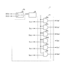
- the control unit 7 of the power conversion device 100 according to the first embodiment includes the drive signals Sup, Sun, Svp, and Svn corresponding to the above-described upper arm switching elements 3a to 3c and the lower arm switching elements 3d to 3f. , Swp, and Swn, in addition to each component (not shown), the overcurrent detection result by the first overcurrent detection unit 21a and the overcurrent detection result by the second overcurrent detection unit 21b are switched.
- Output overcurrent detection result switching unit 25, state holding unit 26 holding the output of overcurrent detection result switching unit 25, and the output of state holding unit 26 is power supply shunt resistor 5 or lower arm shunt resistor 6a,
- Each of the upper arm switching elements 3a constituting the inverter 2 has a value (in this case, Lo output) indicating that an overcurrent has flowed into either 6b or 6c.
- the overcurrent detection result switching unit 25 includes switch means 28 as shown in FIG. In this switch means 28, the output OC1 as the overcurrent detection result of the first overcurrent detection unit 21a and the overcurrent detection result of the second overcurrent detection unit 21b according to the output voltage vector of the inverter 2 described later. A certain output OC2 is switched and output as OC3.
- the state holding unit 26 is configured by, for example, a latch circuit. In this state holding unit 26, the current value of the output OC3 of the overcurrent detection result switching unit 25 flowing through the power supply shunt resistor 5 or the current flowing through the lower arm shunt resistors 6a, 6b, 6c is a normal value.
- Is equal to the output value OC3 of the overcurrent detection result switching unit 25 (here, Hi output), and the output OC3 of the overcurrent detection result switching unit 25 is
- the overcurrent detection result switching unit 25 The same value as the output value OC3 (here, Lo output) is held.
- the inverter drive stop unit 27 includes each AND operation means 29 a, 29 b, 29 c, 29 d, 29 e, 29 f.
- the output OC3 of the overcurrent detection result switching unit 25 held by the state holding unit 26 is the current flowing through the power supply shunt resistor 5 or each phase.
- While the current values of the currents flowing through the lower arm shunt resistors 6a, 6b, and 6c are normal values (here, Hi output), the drive signals Sup, Sun, Svp, Svn, Swp, Swn is output, and the output OC3 of the overcurrent detection result switching unit 25 is a value indicating that an overcurrent has flowed through either the power supply shunt resistor 5 or the lower arm shunt resistors 6a, 6b, 6c (here, Lo Output), the output of each drive signal Sup, Sun, Svp, Svn, Swp, Swn is stopped.
- the present invention is not limited by the configurations and control methods of the first overcurrent detection unit 21a, the second overcurrent detection unit 21b, and the control unit 7 described above.
- FIG. 5 is a diagram showing the relationship between the ON / OFF state of each phase upper arm switching element and the output voltage vector of the inverter in the space vector modulation method.
- FIG. 5A is a schematic diagram showing the relationship between the ON / OFF state of each phase upper arm switching element 3a-3c and the output voltage vector of inverter 2, and
- FIG. 5B shows the output voltage of inverter 2.
- the definition of a vector is shown.
- the upper arm switching elements 3a to 3c of each phase are defined as “1”, and the case of being in the OFF state is defined as “0”.
- the output voltage vector of inverter 2 is ((the state of U phase upper arm switching element 3a) (V phase upper arm switching element). 3b state) (state of W-phase upper arm switching element 3c)) V0 (000), V1 (100), V2 (010), V3 (001), V4 (110), V5 (011) ), V6 (101), and V7 (111).
- V0 (000) and V7 (111) having no magnitude are called zero vectors, and other magnitudes are equal and V1 (100), V2 having the same phase difference of 60 degrees. (010), V3 (001), V4 (110), V5 (011), and V6 (101) are called real vectors.
- the output voltage vector of the inverter in the space vector modulation method by PWM modulation is the zero vectors V0 and V7 having no magnitude and the real vectors V1 to V6 having the same magnitude and a phase difference of 60 °.
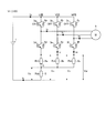
- FIG. 6 is a diagram showing currents that flow through each part of the inverter when the output voltage vector of the inverter is the real vector V1 (100).
- each phase current iu, iv, iw flowing from the high potential side to the low potential side of each phase winding of the load device (motor in this case) 9 is a positive value.
- the description is the same as in FIG.
- the U-phase is directed from the positive voltage side of the DC power supply 1 to the motor 9 via the U-phase upper arm switching element 3a.
- the current iu flows
- the V-phase current iv flows from the motor 9 to the negative voltage side of the DC power supply 1 via the V-phase lower arm switching element 3e, the V-phase lower arm shunt resistor 6b, and the power supply shunt resistor 5, and the W-phase lower A W-phase current iw flows toward the negative voltage side of the DC power supply 1 via the arm switching element 3 f and the power supply shunt resistor 5.
- the U-phase lower arm voltage Vu, the V-phase lower arm voltage Vv, and the W-phase lower arm voltage Vw can be expressed by the following equations (1), (2), and (3).
- the I-phase current iu flowing through the power supply shunt resistance 5 can be calculated using the above equation (1).
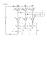
- FIG. 7 is a diagram showing currents that flow through each part of the inverter when the output voltage vector of the inverter is the real vector V2 (010).
- the V-phase is directed from the positive voltage side of the DC power supply 1 to the motor 9 via the V-phase upper arm switching element 3b.
- the current iv flows, the U-phase current iu flows from the motor 9 to the negative voltage side of the DC power supply 1 via the U-phase lower arm switching element 3d, the U-phase lower arm shunt resistor 6a, and the power supply shunt resistor 5, and the W-phase lower A W-phase current iw flows toward the negative voltage side terminal of the DC power supply 1 via the arm switching element 3 f and the power supply shunt resistor 5.
- the U-phase lower arm voltage Vu, the V-phase lower arm voltage Vv, and the W-phase lower arm voltage Vw can be expressed by the following equations (4), (5), and (6).
- the V-phase current iv flowing through the power supply shunt resistance 5 can be calculated using the above equation (5).
- FIG. 8 is a diagram showing currents that flow through each part of the inverter when the output voltage vector of the inverter is the real vector V3 (001).
- the W phase is directed from the positive voltage side of the DC power supply 1 to the motor 9 via the W phase upper arm switching element 3c.
- the current iw flows, the U-phase current iu flows from the motor 9 to the negative voltage side of the DC power supply 1 via the U-phase lower arm switching element 3d, the U-phase lower arm shunt resistor 6a, and the power supply shunt resistor 5, and the V-phase lower A V-phase current iv flows toward the negative voltage side of the DC power supply 1 via the arm switching element 3e and the power supply shunt resistor 5.
- the U-phase lower arm voltage Vu, the V-phase lower arm voltage Vv, and the W-phase lower arm voltage Vw can be expressed by the following equations (7), (8), and (9).
- the W-phase current iw flowing through the power supply shunt resistance 5 can be calculated using the above equation (9).
- the U-phase lower arm voltage Vu and the V-phase lower arm It is possible to calculate each phase current iu, iv, iw flowing in each phase winding of the motor 9 by detecting the voltage Vv and the W-phase lower arm voltage Vw, but using a plurality of detected values. Since time to calculate is necessary, it is not suitable for overcurrent detection that requires immediacy.
- phase current for one phase by detecting the power supply shunt resistance voltage Vx, and the overcurrent detection value of each phase current iu, iv, iw with respect to the power supply shunt resistance voltage Vx. It is possible to detect an overcurrent by simply setting the first threshold value V1 corresponding to, and simply detecting the power supply shunt resistance voltage Vx and comparing it with the first threshold value V1.
- phase currents iu, iv, and iw are obtained without using Kirchhoff's first law and the phase current equilibrium conditions, the present invention is applicable even when the motor 9 has an unbalanced load.
- FIG. 9 is a diagram showing currents that flow through each part of the inverter when the output voltage vector of the inverter is the real vector V4 (110).
- the U-phase is directed from the positive voltage side of the DC power supply 1 to the motor 9 via the U-phase upper arm switching element 3a.
- a current iu flows, and a V-phase current iv flows to the motor 9 via the V-phase upper arm switching element 3b.
- the W-phase lower arm switching element 3f, the W-phase lower arm shunt resistor 6c, and the power supply shunt resistor 5 are transmitted from the motor 9 to the motor 9.
- a W-phase current iw flows toward the negative voltage side of the DC power supply 1 via the DC power supply 1.
- the U-phase lower arm voltage Vu, the V-phase lower arm voltage Vv, and the W-phase lower arm voltage Vw can be expressed by the following equations (10), (11), and (12).
- the W-phase current iw flowing through the power supply shunt resistance 5 can be calculated using the above equation (10) or (11).
- FIG. 10 is a diagram showing currents that flow through each part of the inverter when the output voltage vector of the inverter is the real vector V5 (011).
- the V-phase is directed from the positive voltage side of the DC power supply 1 to the motor 9 via the V-phase upper arm switching element 3b.
- a current iv flows, and a W-phase current iw flows toward the motor 9 via the W-phase upper arm switching element 3c.
- the U-phase lower arm switching element 3d, the U-phase lower arm shunt resistor 6a, and the power supply shunt resistor 5 are transmitted from the motor 9 to the motor 9.
- the U-phase current iu flows toward the negative voltage side of the DC power supply 1 via the via.
- the U-phase lower arm voltage Vu, the V-phase lower arm voltage Vv, and the W-phase lower arm voltage Vw can be expressed by the following equations (14), (16), and (17).
- the U-phase current iu flowing through the power supply shunt resistance 5 can be calculated using the above equation (16) or (17).
- FIG. 11 is a diagram showing currents that flow through each part of the inverter when the output voltage vector of the inverter is the real vector V6 (101).
- the U-phase is directed from the positive voltage side of the DC power supply 1 to the motor 9 via the U-phase upper arm switching element 3a.
- a current iu flows and a W-phase current iw flows toward the motor 9 via the W-phase upper arm switching element 3c, and the V-phase lower arm switching element 3e, the V-phase lower arm shunt resistor 6b, and the power supply shunt resistor 5 are transmitted from the motor 9 to the motor 9.
- the V-phase current iv flows toward the negative voltage side of the DC power supply 1 through the DC voltage.
- the U-phase lower arm voltage Vu, the V-phase lower arm voltage Vv, and the W-phase lower arm voltage Vw can be expressed by the following equations (20), (21), and (22).
- the V-phase current iv flowing through the power supply shunt resistance 5 can be calculated using the above equation (20) or (22).
- the phase currents iu, iv In the power conversion device 100 according to the present embodiment, even when the real vectors are V4 (110), V5 (011), and V6 (101), when the motor 9 is a three-phase balanced load, By detecting any one of the U-phase lower arm voltage Vu, the V-phase lower arm voltage Vv, and the W-phase lower arm voltage Vw, the phase currents iu, iv, Although it is possible to calculate iw, it requires time to calculate using a plurality of detection values, and is not suitable for overcurrent detection that requires immediacy.
- phase current for one phase by detecting the power supply shunt resistance voltage Vx, and the overcurrent detection value of each phase current iu, iv, iw with respect to the power supply shunt resistance voltage Vx. It is possible to detect an overcurrent by simply setting the first threshold value V1 corresponding to, and simply detecting the power supply shunt resistance voltage Vx and comparing it with the first threshold value V1.
- FIG. 12 is a diagram showing currents that flow through each part of the inverter when the output voltage vector of the inverter is zero vector V0 (000).
- the current that flows through the inverter 2 when the real vector V1 (100) shifts to the zero vector V0 (000) is illustrated.
- Vu ( ⁇ iu) ⁇ Rsh (25)
- Vv iv ⁇ Rsh (26)
- Vw iw ⁇ Rsh (27)
- phase currents iu, iv, iw can be calculated using the equations (11), (12).
- the U-phase lower arm voltage Vu, the V-phase lower arm voltage Vv, and the W-phase lower arm voltage Vw are set.
- the phase current for three phases which corresponds to the overcurrent detection value of each phase current iu, iv, iw for each phase lower arm voltage Vu, Vv, Vw.
- the second threshold V2 and the third threshold V3 simply detecting the lower arm voltages Vu, Vv, Vw of each phase and comparing them with the second threshold V2 and the third threshold V3, It is possible to detect overcurrent.
- phase currents iu, iv, and iw can be calculated by using Kirchhoff's first law and equilibrium conditions of phase currents, but the detailed description thereof is omitted here.
- FIG. 13 is a diagram illustrating an example of each output voltage vector generation period in one carrier cycle.
- the zero vector V0 (000) in the period a the real vector V1 (100) in the period b
- the real vector V4 (110) in the period c the zero vector V7 (111) in the period d
- the real vector V4 in the period e. 110
- the a and g periods are zero vectors V0 (000). Therefore, by detecting the U-phase lower arm voltage Vu, the V-phase lower arm voltage Vv, and the W-phase lower arm voltage Vw, It is possible to detect overcurrents of the phase currents iu, iv, iw. That is, in the periods a and g, the second overcurrent detection unit 21b can detect the overcurrents of the phase currents iu, iv and iw.
- the b and f periods are the real vectors V1 (100), it is possible to detect the overcurrent of the I-phase current iu by detecting the power supply shunt resistance voltage Vx. That is, in the period b and f, the first overcurrent detector 21a can detect the overcurrent of the I-phase current iu.
- the c and e periods are the real vectors V4 (110), it is possible to detect the overcurrent of the W-phase current iw by detecting the power shunt resistance voltage Vx. That is, in the periods c and e, the first overcurrent detection unit 21a can detect the overcurrent of the W-phase current iw.
- each output voltage vector generation period in this one carrier cycle is not limited to the example shown in FIG. 13, but at least one kind of real vector And the zero vector.
- the power conversion device 100 in the generation period of each real vector V1 (100), V2 (010), V3 (001), V4 (110), V5 (011), V6 (101).
- the first overcurrent detection unit 21a By detecting the overcurrent for one phase among the phase currents iu, iv, and iw by the first overcurrent detection unit 21a, overcurrent detection without intervening arithmetic processing can be realized, and zero
- the second overcurrent detection unit 21b detects the overcurrent of the phase currents iu, iv, and iw, thereby realizing overcurrent detection that does not involve arithmetic processing. it can.
- the power conversion device 100 includes the first overcurrent detection unit 21a and the second overcurrent detection unit 21b, and the overcurrent detection result by the first overcurrent detection unit 21a and In each output voltage vector generation period other than the zero vector V7 (111), the overcurrent detection of each phase current is performed using any one of the overcurrent detection results by the second overcurrent detection unit 21b.
- overcurrent detection that does not involve arithmetic processing.
- the switch means 28 of the overcurrent detection result switching unit 25 is used. Is controlled to the first overcurrent detection unit 21a side, and the switch means 28 of the overcurrent detection result switching unit 25 is controlled to the second overcurrent detection unit 21b side during the generation period of the zero vector V0 (000).
- the first threshold value set in the first overcurrent detection unit 21a, and the second threshold value and the third threshold value set in the second overcurrent detection unit 21b can be set one by one. That's fine.
- the phase current is always supplied to the power supply shunt resistor 5 or the lower arm of each phase.
- Overcurrent detection result when any one of the current resistors 6a, 6b, 6c is flowing, and when the phase current flows through both the power source shunt resistor 5 and the lower arm shunt resistors 6a, 6b, 6c. Since the detection result can be eliminated, the first threshold value set in the first overcurrent detection unit 21a and the second threshold value set in the second overcurrent detection unit 21b according to the output voltage vector And overcurrent detection can be reliably performed without changing the third threshold value.
- the power shunt resistor provided between the negative voltage side of the DC power source and the inverter, the lower arm switching element of each phase, and the power shunt resistor
- a power shunt resistor that is a voltage between the connection point of the power shunt resistor and each phase lower arm shunt resistor and the negative voltage side (reference potential) of the DC power supply.
- a first overcurrent detector for detecting an overcurrent of the current flowing through the power supply shunt resistor based on the voltage, a connection point between each phase lower arm switching element and each phase lower arm shunt resistor, and a negative voltage side of the DC power supply
- a second overcurrent detection unit that detects overcurrent of each current flowing through each phase lower arm shunt resistor based on each phase lower arm voltage that is each voltage between (reference potential) and Since any one of the overcurrent detection result by the first overcurrent detection unit and the overcurrent detection result by the second overcurrent detection unit is used, the overcurrent detection of each phase current is performed.
- Each phase upper arm switching element is turned ON / OFF, that is, not only when the output voltage vector of the inverter is the zero vector V0 but also when it is the real vectors V1 to V6. Since current overcurrent detection can be performed, the phase current overcurrent detection period can be extended and the overcurrent detection procedure can be simplified, and the operation reliability of the inverter and load device can be improved. it can.
- the switch means of the overcurrent detection result switching unit is the first. Since the switch means of the overcurrent detection result switching unit is controlled to the second overcurrent detection unit 21b side during the generation period of the zero vector V0 (000), This is the overcurrent detection result when the phase current flows through either the power shunt resistor or the lower arm shunt resistor of each phase, and when the phase current flows through both the power shunt resistor and the lower arm shunt resistor of each phase.
- the first threshold value set in the first overcurrent detection unit, and the second threshold value and the third threshold value set in the second overcurrent detection unit are inverters. Without changing in response to the output voltage vector, it is possible to reliably perform the overcurrent detection.
- Embodiment 2 the example in which the overcurrent detection result by the first overcurrent detection unit and the overcurrent detection result by the second overcurrent detection unit are switched according to the output voltage vector of the inverter has been described.
- an example will be described in which the overcurrent detection result by the first overcurrent detection unit and the overcurrent detection result by the second overcurrent detection unit are switched according to the operation state of the inverter or the modulation rate.
- the structure of the power converter device concerning Embodiment 2 is the same as the power converter device concerning Embodiment 1, description is abbreviate
- the switch means 28 of the overcurrent detection result switching unit 25 determines the detection result of the first overcurrent detection unit 21a and the second overcurrent detection according to the operating state of the inverter 2 or the modulation rate. The result is switched and output as OC3.
- FIG. 14 is a diagram showing the transition of the power supply shunt resistance voltage Vx when the modulation rate of the inverter is relatively high.
- FIG. 15 is a diagram showing the transition of the power supply shunt resistance voltage Vx when the modulation rate of the inverter is relatively low.
- FIG. 16 is a diagram showing the transition of the U-phase lower arm voltage Vu when the modulation rate of the inverter is relatively low.
- the switch means 28 in an operation state in which the inverter 2 is operated for a long time in an operation state where the modulation factor is high, the switch means 28 is switched in the generation period of the real vectors V1 (100) to V6 (101). In the operation state where the control is performed to the overcurrent detection unit 21a side of 1 and the detection result (OC1) of the first overcurrent detection unit 21a is selected, and the inverter 2 is operated for a long time in an operation state where the modulation factor is low. In the generation period of the zero vector V0 (000), the switch means 28 is controlled to the second overcurrent detection unit 21b side to select the detection result (OC2) of the second overcurrent detection unit 21b.
- a threshold is provided for the modulation rate of the inverter 2, and when the modulation rate of the inverter 2 is larger than the threshold, in the generation period of the real vectors V1 (100) to V6 (101),
- the switch means 28 is controlled to the first overcurrent detection unit 21a side and the detection result (OC1) of the first overcurrent detection unit 21a is selected, and the modulation rate of the inverter 2 is equal to or less than the threshold value
- the switch The means 28 is controlled to the second overcurrent detection section 21b side, and the switch means 28 is controlled to the second overcurrent detection section 21b side during the generation period of the zero vector V0 (000) to detect the second overcurrent.
- the detection result (OC2) of the unit 21b is selected.
- the switch means 28 is controlled to be off, and any detection result is not selected, and the operation state where the inverter 2 is operated for a long time in the operation condition where the modulation factor is low, or the modulation factor of the inverter 2 is the threshold value.
- the switch means 28 is turned off, and any detection result is not selected.
- the first threshold value set in the first overcurrent detection unit, and the second threshold value and the third threshold value set in the second overcurrent detection unit without being changed in accordance with the output voltage vector of the inverter 2, the detection result by the output voltage vector having a short generation period can be eliminated, and the accuracy of overcurrent detection can be improved.
- the overcurrent detection result by the first overcurrent detection unit and the second overcurrent detection unit according to the operation state of the inverter or the modulation rate.
- the overcurrent detection result is switched to the actual vector V1 (100) when the operation state is such that the inverter is operated for a long time in the operation condition where the modulation rate of the inverter is high, or when the modulation rate of the inverter is larger than the threshold value.
- the switch means of the overcurrent detection result switching unit is controlled to the first overcurrent detection unit side to select the detection result of the first overcurrent detection unit, and the zero vector V0 (000) is an operation state in which the switch means of the overcurrent detection result switching unit is turned off and no detection result is selected, and the inverter is operated for a long time in an operating condition with a low modulation rate.
- the switch means of the overcurrent detection result switching unit is controlled to the second overcurrent detection unit side during the generation period of the zero vector V0 (000).
- the switch means of the overcurrent detection result switching unit is controlled to be off during the generation period of the real vectors V1 (100) to V6 (101). Since the selection is not performed, the first threshold value set in the first overcurrent detection unit, the second threshold value set in the second overcurrent detection unit, and the third threshold value are set as in the first embodiment. Without changing the threshold value according to the output voltage vector of the inverter, the detection result based on the output voltage vector having a short generation period can be eliminated, and the accuracy of overcurrent detection can be improved.
- control unit includes the overcurrent detection result switching unit, the state holding unit, and the inverter drive stop unit.
- the overcurrent detection port of the control unit can be reduced to one by providing the overcurrent detection result switching unit outside the control unit.
- control unit it is also possible to simplify the configuration of the control unit by providing a latch circuit constituting the state holding unit outside the control unit.
- each phase upper arm switching element and each phase lower arm switching element may be driven based on a logical product calculation result of each drive signal and the output of the state holding unit.
- each phase upper arm switching element and each phase may be calculated based on the logical product operation result of the gate signal of each phase upper arm switching element and each phase lower arm switching element generated based on each drive signal and the output of the state holding unit.
- the lower arm switching element may be driven.
- the power converter device demonstrated in embodiment mentioned above is applied to the motor drive device which uses a motor as a load
- This motor drive device is applied to air blowers and compressors, such as an air conditioner, a refrigerator, and a refrigerator. Needless to say, it is possible to improve the operational reliability of these devices and devices.
- the second threshold value for each lower arm voltage and the third threshold value higher than the second threshold value are set in each phase voltage comparison unit, and each lower arm voltage is set to the first threshold voltage.
- the threshold value is equal to or greater than 2 and equal to or less than the third threshold value
- a value indicating that the current value of each current flowing through each lower arm shunt resistor is a normal value is output.
- the voltage is smaller than the second threshold value or larger than the third threshold value, an example in which a value indicating that an overcurrent has flowed through each lower arm shunt resistor has been described.
- the current value of each current flowing through each lower arm shunt resistor is determined when each lower arm voltage is equal to or higher than the second threshold value.
- a value indicating a normal value is output, and when each lower arm voltage is smaller than the second threshold value, a value indicating that an overcurrent has passed through each lower arm shunt resistor is output. That's fine.
- the current of each current flowing through each phase lower arm shunt resistor when each phase lower arm voltage is equal to or lower than the third threshold value when each phase lower arm voltage is equal to or lower than the third threshold value.
- a value indicating that the value is a normal value is output, and when each lower arm voltage is greater than the third threshold value, a value indicating that an overcurrent has passed through each lower arm shunt resistor is output. You can do it.
- the power conversion device As described above, the power conversion device according to the present invention, the motor driving device including the power conversion device, the blower and the compressor including the power conversion device, the air conditioner including the same, the refrigerator, and the refrigerator include PWM modulation. This is useful for a configuration equipped with a three-phase inverter of the type, and in particular, the phase current overcurrent detection period is extended and the overcurrent detection procedure is simplified to improve the operation reliability of each device and each device. Suitable as a technology that can.
Landscapes
- Engineering & Computer Science (AREA)
- Power Engineering (AREA)
- Mechanical Engineering (AREA)
- General Engineering & Computer Science (AREA)
- Physics & Mathematics (AREA)
- Thermal Sciences (AREA)
- Inverter Devices (AREA)
Abstract
Priority Applications (5)
| Application Number | Priority Date | Filing Date | Title |
|---|---|---|---|
| CN201380075039.3A CN105052026B (zh) | 2013-04-08 | 2013-04-08 | 电力转换装置、电动机驱动装置、鼓风机、压缩机、空调机、冰箱及制冷机 |
| US14/781,064 US9647604B2 (en) | 2013-04-08 | 2013-04-08 | Power conversion device, motor drive device including power conversion device, air blower and compressor including motor drive device, and air conditioner, refrigerator, and freezer including air blower and compressor |
| HK16100565.7A HK1212825B (en) | 2013-04-08 | Power conversion device, motor drive device , ventilator, compressor, air conditioner, refrigerator and freezer | |
| PCT/JP2013/060619 WO2014167625A1 (fr) | 2013-04-08 | 2013-04-08 | Dispositif de conversion d'énergie, dispositif motorisé comprenant le même dispositif, ventilateur comprenant le même dispositif, compresseur, et climatiseur, réfrigérateur, et congélateur comprenant les mêmes dispositifs |
| JP2015510972A JP6038291B2 (ja) | 2013-04-08 | 2013-04-08 | 電力変換装置、およびそれを備えたモータ駆動装置、およびそれを備えた送風機、圧縮機、およびそれらを備えた空気調和機、冷蔵庫、ならびに冷凍機 |
Applications Claiming Priority (1)
| Application Number | Priority Date | Filing Date | Title |
|---|---|---|---|
| PCT/JP2013/060619 WO2014167625A1 (fr) | 2013-04-08 | 2013-04-08 | Dispositif de conversion d'énergie, dispositif motorisé comprenant le même dispositif, ventilateur comprenant le même dispositif, compresseur, et climatiseur, réfrigérateur, et congélateur comprenant les mêmes dispositifs |
Publications (1)
| Publication Number | Publication Date |
|---|---|
| WO2014167625A1 true WO2014167625A1 (fr) | 2014-10-16 |
Family
ID=51689062
Family Applications (1)
| Application Number | Title | Priority Date | Filing Date |
|---|---|---|---|
| PCT/JP2013/060619 Ceased WO2014167625A1 (fr) | 2013-04-08 | 2013-04-08 | Dispositif de conversion d'énergie, dispositif motorisé comprenant le même dispositif, ventilateur comprenant le même dispositif, compresseur, et climatiseur, réfrigérateur, et congélateur comprenant les mêmes dispositifs |
Country Status (4)
| Country | Link |
|---|---|
| US (1) | US9647604B2 (fr) |
| JP (1) | JP6038291B2 (fr) |
| CN (1) | CN105052026B (fr) |
| WO (1) | WO2014167625A1 (fr) |
Families Citing this family (6)
| Publication number | Priority date | Publication date | Assignee | Title |
|---|---|---|---|---|
| DE102014223236A1 (de) * | 2014-11-14 | 2016-05-19 | Robert Bosch Gmbh | Stromrichter und Verfahren zum Betreiben eines Stromrichters |
| JP6583000B2 (ja) * | 2016-01-07 | 2019-10-02 | 株式会社デンソー | 回転電機の制御装置 |
| WO2017183208A1 (fr) * | 2016-04-22 | 2017-10-26 | 三菱電機株式会社 | Dispositif de conversion de puissance |
| JP6638616B2 (ja) * | 2016-09-30 | 2020-01-29 | 株式会社デンソー | 電源制御装置 |
| CN106877784B (zh) * | 2017-03-08 | 2020-05-26 | 苏州汇川技术有限公司 | 一种电机控制器保护装置及方法 |
| CN114556775B (zh) * | 2019-10-24 | 2025-07-15 | 三菱电机株式会社 | 马达驱动系统以及空调机 |
Citations (8)
| Publication number | Priority date | Publication date | Assignee | Title |
|---|---|---|---|---|
| JPH0217868A (ja) * | 1988-07-06 | 1990-01-22 | Hitachi Ltd | インバータの異常判別回路 |
| JPH05207766A (ja) * | 1992-01-23 | 1993-08-13 | Mitsubishi Electric Corp | 過電流保護方法及びその装置及び過電流検出装置 |
| JPH0993948A (ja) * | 1995-09-26 | 1997-04-04 | Mitsubishi Electric Corp | モータの制御装置 |
| JP2005033875A (ja) * | 2003-07-09 | 2005-02-03 | Fuji Electric Fa Components & Systems Co Ltd | モータ駆動装置 |
| JP2005304176A (ja) * | 2004-04-12 | 2005-10-27 | Matsushita Electric Ind Co Ltd | モータ駆動装置 |
| JP2006067747A (ja) * | 2004-08-30 | 2006-03-09 | Matsushita Electric Ind Co Ltd | インバータ装置 |
| JP2006101685A (ja) * | 2004-08-31 | 2006-04-13 | Matsushita Electric Ind Co Ltd | インバータ装置 |
| JP2011045218A (ja) * | 2009-08-24 | 2011-03-03 | Mitsubishi Electric Corp | 電力変換装置、それを備えたモーター駆動制御装置、それを搭載した圧縮機及び送風機、並びに、その圧縮機又は送風機を搭載した空気調和機、冷蔵庫及び冷凍庫 |
Family Cites Families (11)
| Publication number | Priority date | Publication date | Assignee | Title |
|---|---|---|---|---|
| US3912980A (en) * | 1974-03-20 | 1975-10-14 | Air Prod & Chem | Direct current arc power supply |
| EP0431492B1 (fr) * | 1989-12-04 | 1996-01-24 | Kabushiki Kaisha Toshiba | Convertisseur de puissance de type pont avec rendement amélioré |
| JP2003209976A (ja) | 2002-01-11 | 2003-07-25 | Matsushita Electric Ind Co Ltd | Pwmインバータ装置及びその電流検出方法 |
| JP4350623B2 (ja) * | 2004-09-13 | 2009-10-21 | 本田技研工業株式会社 | 制御装置 |
| JP2007236188A (ja) | 2006-02-06 | 2007-09-13 | Matsushita Electric Ind Co Ltd | インバータ装置 |
| JP4177392B2 (ja) * | 2006-06-08 | 2008-11-05 | 三菱電機株式会社 | 半導体電力変換装置 |
| JP2011015472A (ja) * | 2009-06-30 | 2011-01-20 | Sanyo Electric Co Ltd | インバータ装置 |
| JP2011050183A (ja) | 2009-08-27 | 2011-03-10 | Sanyo Electric Co Ltd | インバータ装置 |
| JP5333422B2 (ja) * | 2010-12-07 | 2013-11-06 | 株式会社デンソー | 電力変換装置 |
| CN103348579A (zh) * | 2011-03-14 | 2013-10-09 | 日立工机株式会社 | 逆变设备和电动工具 |
| JP5814065B2 (ja) * | 2011-10-03 | 2015-11-17 | 株式会社マキタ | モータ電流検出装置、モータ制御装置、及び電動工具 |
-
2013
- 2013-04-08 CN CN201380075039.3A patent/CN105052026B/zh not_active Expired - Fee Related
- 2013-04-08 JP JP2015510972A patent/JP6038291B2/ja not_active Expired - Fee Related
- 2013-04-08 WO PCT/JP2013/060619 patent/WO2014167625A1/fr not_active Ceased
- 2013-04-08 US US14/781,064 patent/US9647604B2/en not_active Expired - Fee Related
Patent Citations (8)
| Publication number | Priority date | Publication date | Assignee | Title |
|---|---|---|---|---|
| JPH0217868A (ja) * | 1988-07-06 | 1990-01-22 | Hitachi Ltd | インバータの異常判別回路 |
| JPH05207766A (ja) * | 1992-01-23 | 1993-08-13 | Mitsubishi Electric Corp | 過電流保護方法及びその装置及び過電流検出装置 |
| JPH0993948A (ja) * | 1995-09-26 | 1997-04-04 | Mitsubishi Electric Corp | モータの制御装置 |
| JP2005033875A (ja) * | 2003-07-09 | 2005-02-03 | Fuji Electric Fa Components & Systems Co Ltd | モータ駆動装置 |
| JP2005304176A (ja) * | 2004-04-12 | 2005-10-27 | Matsushita Electric Ind Co Ltd | モータ駆動装置 |
| JP2006067747A (ja) * | 2004-08-30 | 2006-03-09 | Matsushita Electric Ind Co Ltd | インバータ装置 |
| JP2006101685A (ja) * | 2004-08-31 | 2006-04-13 | Matsushita Electric Ind Co Ltd | インバータ装置 |
| JP2011045218A (ja) * | 2009-08-24 | 2011-03-03 | Mitsubishi Electric Corp | 電力変換装置、それを備えたモーター駆動制御装置、それを搭載した圧縮機及び送風機、並びに、その圧縮機又は送風機を搭載した空気調和機、冷蔵庫及び冷凍庫 |
Also Published As
| Publication number | Publication date |
|---|---|
| CN105052026A (zh) | 2015-11-11 |
| US9647604B2 (en) | 2017-05-09 |
| JPWO2014167625A1 (ja) | 2017-02-16 |
| JP6038291B2 (ja) | 2016-12-07 |
| HK1212825A1 (zh) | 2016-06-17 |
| US20160049896A1 (en) | 2016-02-18 |
| CN105052026B (zh) | 2017-12-05 |
Similar Documents
| Publication | Publication Date | Title |
|---|---|---|
| JP6138276B2 (ja) | 電力変換装置、およびそれを備えたモータ駆動装置、およびそれを備えた送風機、圧縮機、およびそれらを備えた空気調和機、冷蔵庫、ならびに冷凍機 | |
| JP6038291B2 (ja) | 電力変換装置、およびそれを備えたモータ駆動装置、およびそれを備えた送風機、圧縮機、およびそれらを備えた空気調和機、冷蔵庫、ならびに冷凍機 | |
| JP6410829B2 (ja) | 電力変換装置、それを備えたモータ駆動装置、送風機および圧縮機、ならびに、それらの少なくとも一方を備えた空気調和機、冷蔵庫および冷凍機 | |
| US8604732B2 (en) | Inverter unit | |
| JP6333563B2 (ja) | インバータ制御装置およびそれを用いた冷凍装置 | |
| JP5505042B2 (ja) | 中性点昇圧方式の直流−三相変換装置 | |
| WO2014167714A1 (fr) | Dispositif de conversion d'énergie, dispositif pilote de moteur pourvu de ce dernier, ventilateur pourvu dudit dispositif pilote de moteur, compresseur ainsi que conditionneur d'air, réfrigérateur et congélateur pourvu dudit ventilateur et dudit compresseur | |
| JP6134813B2 (ja) | 電力変換装置および電力変換装置の制御方法 | |
| KR101514391B1 (ko) | 벡터 제어 장치, 및 그것을 사용한 모터 제어 장치, 공조기 | |
| WO2014097804A1 (fr) | Dispositif onduleur | |
| JP2010098820A (ja) | 電力変換装置 | |
| CN107112922B (zh) | 变流器和用于运行变流器的方法 | |
| JP6157599B2 (ja) | 電力変換装置、およびそれを備えたモータ駆動装置、およびそれを備えた送風機、圧縮機、およびそれらを備えた空気調和機、冷蔵庫、ならびに冷凍機 | |
| JP2019187151A (ja) | 電力変換装置 | |
| JP2006238637A (ja) | インバータ装置 | |
| JP5895704B2 (ja) | 電力変換装置 | |
| JP6707298B2 (ja) | 電力変換装置 | |
| HK1212825B (en) | Power conversion device, motor drive device , ventilator, compressor, air conditioner, refrigerator and freezer |
Legal Events
| Date | Code | Title | Description |
|---|---|---|---|
| WWE | Wipo information: entry into national phase |
Ref document number: 201380075039.3 Country of ref document: CN |
|
| 121 | Ep: the epo has been informed by wipo that ep was designated in this application |
Ref document number: 13881836 Country of ref document: EP Kind code of ref document: A1 |
|
| ENP | Entry into the national phase |
Ref document number: 2015510972 Country of ref document: JP Kind code of ref document: A |
|
| WWE | Wipo information: entry into national phase |
Ref document number: 14781064 Country of ref document: US |
|
| NENP | Non-entry into the national phase |
Ref country code: DE |
|
| 122 | Ep: pct application non-entry in european phase |
Ref document number: 13881836 Country of ref document: EP Kind code of ref document: A1 |