WO2014167875A1 - Dispositif d'usinage laser et système de production de dispositif d'affichage optique - Google Patents
Dispositif d'usinage laser et système de production de dispositif d'affichage optique Download PDFInfo
- Publication number
- WO2014167875A1 WO2014167875A1 PCT/JP2014/051682 JP2014051682W WO2014167875A1 WO 2014167875 A1 WO2014167875 A1 WO 2014167875A1 JP 2014051682 W JP2014051682 W JP 2014051682W WO 2014167875 A1 WO2014167875 A1 WO 2014167875A1
- Authority
- WO
- WIPO (PCT)
- Prior art keywords
- optical member
- cutting
- bonding
- member sheet
- optical
- Prior art date
- Legal status (The legal status is an assumption and is not a legal conclusion. Google has not performed a legal analysis and makes no representation as to the accuracy of the status listed.)
- Ceased
Links
Images







Classifications
-
- B—PERFORMING OPERATIONS; TRANSPORTING
- B23—MACHINE TOOLS; METAL-WORKING NOT OTHERWISE PROVIDED FOR
- B23K—SOLDERING OR UNSOLDERING; WELDING; CLADDING OR PLATING BY SOLDERING OR WELDING; CUTTING BY APPLYING HEAT LOCALLY, e.g. FLAME CUTTING; WORKING BY LASER BEAM
- B23K26/00—Working by laser beam, e.g. welding, cutting or boring
- B23K26/36—Removing material
- B23K26/38—Removing material by boring or cutting
-
- B—PERFORMING OPERATIONS; TRANSPORTING
- B23—MACHINE TOOLS; METAL-WORKING NOT OTHERWISE PROVIDED FOR
- B23K—SOLDERING OR UNSOLDERING; WELDING; CLADDING OR PLATING BY SOLDERING OR WELDING; CUTTING BY APPLYING HEAT LOCALLY, e.g. FLAME CUTTING; WORKING BY LASER BEAM
- B23K26/00—Working by laser beam, e.g. welding, cutting or boring
- B23K26/14—Working by laser beam, e.g. welding, cutting or boring using a fluid stream, e.g. a jet of gas, in conjunction with the laser beam; Nozzles therefor
- B23K26/142—Working by laser beam, e.g. welding, cutting or boring using a fluid stream, e.g. a jet of gas, in conjunction with the laser beam; Nozzles therefor for the removal of by-products
-
- B—PERFORMING OPERATIONS; TRANSPORTING
- B23—MACHINE TOOLS; METAL-WORKING NOT OTHERWISE PROVIDED FOR
- B23K—SOLDERING OR UNSOLDERING; WELDING; CLADDING OR PLATING BY SOLDERING OR WELDING; CUTTING BY APPLYING HEAT LOCALLY, e.g. FLAME CUTTING; WORKING BY LASER BEAM
- B23K26/00—Working by laser beam, e.g. welding, cutting or boring
- B23K26/36—Removing material
- B23K26/361—Removing material for deburring or mechanical trimming
-
- B—PERFORMING OPERATIONS; TRANSPORTING
- B23—MACHINE TOOLS; METAL-WORKING NOT OTHERWISE PROVIDED FOR
- B23K—SOLDERING OR UNSOLDERING; WELDING; CLADDING OR PLATING BY SOLDERING OR WELDING; CUTTING BY APPLYING HEAT LOCALLY, e.g. FLAME CUTTING; WORKING BY LASER BEAM
- B23K26/00—Working by laser beam, e.g. welding, cutting or boring
- B23K26/36—Removing material
- B23K26/40—Removing material taking account of the properties of the material involved
-
- B—PERFORMING OPERATIONS; TRANSPORTING
- B23—MACHINE TOOLS; METAL-WORKING NOT OTHERWISE PROVIDED FOR
- B23K—SOLDERING OR UNSOLDERING; WELDING; CLADDING OR PLATING BY SOLDERING OR WELDING; CUTTING BY APPLYING HEAT LOCALLY, e.g. FLAME CUTTING; WORKING BY LASER BEAM
- B23K2103/00—Materials to be soldered, welded or cut
- B23K2103/16—Composite materials
- B23K2103/166—Multilayered materials
- B23K2103/172—Multilayered materials wherein at least one of the layers is non-metallic
-
- G—PHYSICS
- G02—OPTICS
- G02F—OPTICAL DEVICES OR ARRANGEMENTS FOR THE CONTROL OF LIGHT BY MODIFICATION OF THE OPTICAL PROPERTIES OF THE MEDIA OF THE ELEMENTS INVOLVED THEREIN; NON-LINEAR OPTICS; FREQUENCY-CHANGING OF LIGHT; OPTICAL LOGIC ELEMENTS; OPTICAL ANALOGUE/DIGITAL CONVERTERS
- G02F1/00—Devices or arrangements for the control of the intensity, colour, phase, polarisation or direction of light arriving from an independent light source, e.g. switching, gating or modulating; Non-linear optics
- G02F1/01—Devices or arrangements for the control of the intensity, colour, phase, polarisation or direction of light arriving from an independent light source, e.g. switching, gating or modulating; Non-linear optics for the control of the intensity, phase, polarisation or colour
- G02F1/13—Devices or arrangements for the control of the intensity, colour, phase, polarisation or direction of light arriving from an independent light source, e.g. switching, gating or modulating; Non-linear optics for the control of the intensity, phase, polarisation or colour based on liquid crystals, e.g. single liquid crystal display cells
- G02F1/1303—Apparatus specially adapted to the manufacture of LCDs
Definitions
- the present invention relates to a laser processing apparatus and an optical display device production system.
- This application claims priority based on Japanese Patent Application No. 2013-80846 filed on April 8, 2013 and Japanese Patent Application No. 2013-104400 filed on May 16, 2013, The contents are incorporated herein.
- Patent Document 1 a decomposition product (fume) generated from a laser irradiation portion at the time of laser processing of a product is sucked and removed by a suction device in which a suction port is disposed in the vicinity of the laser irradiation portion.
- a suction device in which a suction port is disposed in the vicinity of the laser irradiation portion.
- Techniques for reducing adhesion are disclosed.
- Patent Document 2 in a method of cutting an optical film with a separator into a predetermined length and pasting it to a product panel, the laser optical axis is tilted from the front to the rear in the laser traveling direction and cut when the film is laser cut.
- An air nozzle that blows hot air toward the part and a smoke collection duct that removes gas generated from the cutting part conveyed by the hot air are integrated with the laser irradiation device, so that the fume on the film surface Techniques for reducing adhesion are disclosed.
- An aspect of the present invention has been made in view of the above circumstances, and provides a laser processing apparatus and an optical display device production system capable of effectively suppressing fume adhesion to a product surface without affecting product processing accuracy.
- the purpose is to do.
- a laser processing apparatus and an optical display device production system employ the following configurations.
- (1) One embodiment of the present invention is a laser processing apparatus that irradiates a processing position of a workpiece with laser light to perform processing, and opens a suction port over the entire length of the processing position in the vicinity of the processing position. A suction device is provided.
- the processing position is provided endlessly on the outer periphery of the specific area of the workpiece, and the suction device is provided so as to surround the entire periphery of the specific area. Also good. In this case, the fumes can be removed by suction without leakage over the entire circumference of the specific region.
- the suction device may be capable of moving forward and backward with respect to the processing position. In this case, laser processing of workpieces having different processing positions can be easily handled.
- the suction device includes a blowout port that blows air toward a product surface between the processing position and the suction port. Also good. In this case, fume adhesion to the product surface between the processing position and the suction port can be suppressed.
- the suction device may blow out warm air from the outlet. In this case, fume adhesion to the product surface between the cutting line and the suction port can be more effectively suppressed.
- Another aspect of the present invention is an optical display device production system configured by bonding an optical member to an optical display component, and the optical display component is larger than a display area of the optical display component.
- a bonding device that bonds the optical member sheet to form a bonded body, and separates the facing portion of the bonding member from the display area of the optical member sheet and the surplus portion outside the facing portion.
- a cutting device for forming the optical member having a size corresponding to the display area, and the cutting device is directed to a cutting portion between the facing portion and the surplus portion of the optical member sheet in the bonded body.
- a laser beam irradiation device that irradiates a laser beam for cutting processing, and a suction device that opens a suction port over the entire length of the cutting portion in the vicinity of the cutting portion.
- the optical member of the size corresponding to a display area is cut
- cutting using laser light is more accurate than cutting using a cutting blade, and the frame portion around the display area can be narrower than when using a cutting blade.
- the effective area of the optical member sheet (optical member) to be left on the optical display component without causing a taper angle (an angle with respect to the direction orthogonal to the bonding surface) due to the inclination of the laser beam at the cut end of the optical member sheet. Can contribute to further narrowing the frame of the device. Further, the fumes generated by the laser processing can be sucked without leakage over the entire length of the processing position, so that the fume can be prevented from adhering to the product surface, and line contamination due to the fumes adhering to the product can be prevented.
- the “part facing the display area” in the above configuration is an area that is not less than the size of the display area and not more than the size of the outer shape (contour shape in plan view) of the optical display component, and the electrical component mounting portion.
- the area where functional parts such as are avoided is shown. That is, the said structure includes the case where the surplus part is laser-cut along the outer periphery of an optical display component.
- the “size corresponding to the display area” in the above configuration is a size not less than the size of the display area and not more than the size of the outer shape (contour shape in plan view) of the optical display component, and It refers to a size that avoids a functional part such as an electric part mounting part in an optical display part.
- the bonded body includes a detection unit that detects an outer peripheral edge of a bonding surface between the optical member sheet and the optical display component, and the cutting portion is connected to the outer peripheral edge. You may set along.
- the “bonding surface between the optical member sheet and the optical display component” in the above configuration refers to a surface facing the optical member sheet of the optical display component, and specifically, “the outer peripheral edge of the bonding surface” In the optical display component, the outer peripheral edge of the substrate on which the optical member sheet is bonded is indicated.
- FIG. 6 is a cross-sectional view taken along line AA in FIG. 5. It is sectional drawing of the double-sided bonding panel which passed through the film bonding system.
- This embodiment demonstrates the film bonding system which comprises the one part as a production system of an optical display device.
- an XYZ orthogonal coordinate system is set.
- the X direction indicates the width direction of the optical display component (liquid crystal panel).
- the Y direction indicates the conveyance direction of the optical display component.
- the Z direction indicates a direction orthogonal to the X direction and the Y direction.
- FIG. 1 shows a schematic configuration of a film bonding system (an optical display device production system) 1 according to the present embodiment.
- the film bonding system 1 bonds a film-shaped optical member such as a polarizing film, a retardation film, and a brightness enhancement film to a panel-shaped optical display component such as a liquid crystal panel or an organic EL panel.
- the film bonding system 1 manufactures an optical member bonding body including an optical display component and an optical member.
- the liquid crystal panel P is used as an optical display component.
- Each part of the film bonding system 1 is comprehensively controlled by a control device 20 as an electronic control device.
- the film bonding system 1 sequentially performs a predetermined process on the liquid crystal panel P while transporting the liquid crystal panel P from the start position to the end position of the bonding process using, for example, a driving roller conveyor 5.
- the liquid crystal panel P is conveyed on the roller conveyor 5 with its front and back surfaces being horizontal.
- the left side shows the upstream side in the transport direction of the liquid crystal panel P (hereinafter referred to as the panel transport upstream side).
- the right side in the figure shows the downstream side of the liquid crystal panel P in the transport direction (hereinafter referred to as the panel transport downstream side).
- the liquid crystal panel P has a rectangular shape in plan view.
- a display region P4 having an outer shape along the outer peripheral edge is formed on the inner side of the outer peripheral edge of the liquid crystal panel P by a predetermined width.
- the liquid crystal panel P is transported in a direction in which the short side of the display region P4 is substantially aligned with the transport direction on the upstream side of the panel transport from the second alignment device 14 described later.
- the liquid crystal panel P is transported in a direction in which the long side of the display region P4 is substantially aligned with the transport direction on the panel transport downstream side of the second alignment device 14.
- a first optical member F11 cut out from the long strip-shaped first optical member sheet F1 and a second optical member F12 cut out from the long strip-shaped second optical member sheet F2.
- seat F3 is bonded.
- polarizing films are bonded to both the backlight side and the display surface side of the liquid crystal panel P, respectively.
- a first optical member (optical member, specific region, facing portion) F11 is bonded as a polarizing film.
- a third optical member (an optical member, a specific region, a facing portion) F13 is bonded to the surface on the display surface side of the liquid crystal panel P as a polarizing film.
- a second optical member (an optical member, a specific region, a facing portion) F12 as a brightness enhancement film is further bonded to the first optical member F11.
- the film bonding system 1 includes a first alignment device 11 that transports the liquid crystal panel P from the upstream process to the panel transport upstream side of the roller conveyor 5 and aligns the liquid crystal panel P.
- the 1st bonding apparatus (bonding apparatus) 12 provided in the panel conveyance downstream rather than the alignment apparatus 11, the 1st cutting apparatus 13 provided in proximity to the 1st bonding apparatus 12, and the 1st bonding apparatus 12 And a second alignment device 14 provided on the downstream side of the panel conveyance with respect to the first cutting device 13.
- the film bonding system 1 is the 2nd bonding apparatus (bonding apparatus) 15 provided in the panel conveyance downstream rather than the 2nd alignment apparatus 14, and the 2nd provided in proximity to the 2nd bonding apparatus 15.
- a cutting device (cutting device) 16 a third alignment device 17 provided on the downstream side of the panel transport relative to the second bonding device 15 and the second cutting device 16, and a downstream side of the panel transport relative to the third alignment device 17
- the 3rd bonding apparatus (bonding apparatus) 18 and the 3rd cutting apparatus (cutting apparatus) 19 provided in proximity to the 3rd bonding apparatus 18 are provided.
- the first alignment device 11 holds the liquid crystal panel P and conveys it freely in the vertical and horizontal directions, and, for example, a camera (not shown) that images the upstream and downstream ends of the liquid crystal panel P. Have.
- the imaging data of this camera is sent to the control device 20.
- the control device 20 operates the first alignment device 11 based on the imaging data and the inspection data in the optical axis direction stored in advance.
- a second alignment device 14 and a third alignment device 17 to be described later also have a camera, and use image data of this camera for alignment.
- the first alignment device 11 is controlled by the control device 20 to perform alignment of the liquid crystal panel P with respect to the first bonding device 12.
- the liquid crystal panel P is positioned in a horizontal direction (hereinafter referred to as a component width direction) orthogonal to the transport direction and in a rotation direction around the vertical axis (hereinafter simply referred to as a rotation direction).
- the liquid crystal panel P is introduced into the bonding position of the first bonding apparatus 12.
- the 1st bonding apparatus 12 is the upper surface of liquid crystal panel P conveyed below the lower surface of the elongate 1st optical member sheet
- the 1st bonding apparatus 12 unwinds the 1st optical member sheet
- a conveying device 12a that conveys along the longitudinal direction, and a pressure roll 12b that bonds the upper surface of the liquid crystal panel P conveyed by the roller conveyor 5 to the lower surface of the first optical member sheet F1 conveyed by the conveying device 12a.
- the transport device 12a holds the first original roll R1 around which the first optical member sheet F1 is wound, and rolls out the first optical member sheet F1 along the longitudinal direction of the first optical member sheet F1.
- recovery part 12d which collect
- the pinching roll 12b has a pair of laminating rollers that are arranged with their axial directions parallel to each other. A predetermined gap is formed between the pair of bonding rollers, and the inside of this gap is the bonding position of the first bonding apparatus 12. In this gap, the liquid crystal panel P and the first optical member sheet F1 are overlapped and introduced. The liquid crystal panel P and the first optical member sheet F1 are sent to the downstream side of the panel conveyance while being pressed between the bonding rollers. Thereby, the 1st bonding sheet
- the 1st cutting device 13 is located in a panel conveyance downstream rather than the pf collection
- a predetermined portion (between the liquid crystal panels P arranged in the transport direction) of the first optical member sheet F1 is cut over the entire width in the component width direction.
- the first cutting device 13 can use a cutting blade. Alternatively, the first cutting device 13 can use a laser cutter.
- the 1st single-sided bonding panel (optical display component, bonding body) P11 by which the sheet piece F1S larger than the display area P4 was bonded on the upper surface of liquid crystal panel P is formed (refer FIG. 4).
- the size of the portion that protrudes outside the liquid crystal panel P (the size of the surplus portion of the sheet piece F1S) is appropriately set according to the size of the liquid crystal panel P.
- the distance between one side of the sheet piece F1S and one side of the liquid crystal panel P is 2 mm at each side of the sheet piece F1S. Set to a length in the range of ⁇ 5 mm.
- the second alignment device 14 is arranged so that the first single-sided bonding panel P11 that has been transported substantially parallel to the short side of the display region P4 is transported substantially parallel to the long side of the display region P4. Convert. In addition, this direction change is performed when the optical axis direction of the other optical member sheet
- the second alignment device 14 performs the same alignment as the first alignment device 11. That is, the second alignment device 14 is based on the inspection data in the optical axis direction stored in the control device 20 and the imaging data of the camera in the component width direction of the first single-sided bonding panel P11 with respect to the second bonding device 15. Positioning and positioning in the rotation direction are performed. In this state, the first single-sided bonding panel P ⁇ b> 11 is introduced into the bonding position of the second bonding device 15.
- the 2nd bonding apparatus 15 is conveyed below the 2nd optical member sheet
- the upper surface of the first single-sided bonding panel P11 (the backlight side of the liquid crystal panel P) is bonded (see FIG. 4).
- the 2nd bonding apparatus 15 unwinds the 2nd optical member sheet
- a conveying device 15a that conveys along the longitudinal direction, and a pinching roll that bonds the upper surface of the first single-sided bonding panel P11 conveyed by the roller conveyor 5 to the lower surface of the second optical member sheet F2 conveyed by the conveying device 15a. 15b.
- the transport device 15a holds the second original roll R2 around which the second optical member sheet F2 is wound, and rolls out the second optical member sheet F2 along the longitudinal direction of the second optical member sheet F2. And a second collection portion 15d that is located on the downstream side of the panel conveyance with respect to the pinching roll 15b and collects an excess portion of the second optical member sheet F2 that has passed through the second cutting device 16.
- the pinching roll 15b has a pair of laminating rollers arranged with their axial directions parallel to each other. A predetermined gap is formed between the pair of bonding rollers, and the inside of this gap is the bonding position of the second bonding apparatus 15. In this gap, the first single-sided bonding panel P11 and the second optical member sheet F2 are overlapped and introduced. The 1st single-sided bonding panel P11 and the 2nd optical member sheet
- the 2nd cutting device 16 is located in the panel conveyance downstream rather than the pinching roll 15b, and the 1st optical of the 1st single-sided bonding panel P11 bonded to the lower surface of the 2nd optical member sheet
- the sheet piece F1S (see FIG. 4) of the member sheet F1 is simultaneously cut.
- the second cutting device 16 is, for example, a CO2 laser cutter, and ends the second optical member sheet F2 and the sheet piece F1S along the outer peripheral edge of the display region P4 (in the present embodiment, along the outer peripheral edge of the liquid crystal panel P). (See FIG. 5).
- the accuracy in the optical axis direction of the first optical member sheet F1 and the second optical member sheet F2 is increased.
- there is no deviation in the optical axis direction between the first optical member sheet F1 and the second optical member sheet F2 is simplified.
- the 2nd single-sided bonding panel (optical display component, bonding body) P12 by which the 1st optical member F11 and the 2nd optical member F12 overlapped and bonded on the upper surface of liquid crystal panel P formed. (See FIG. 6).
- the surplus portion Y of the member sheet F1 and the surplus portion Y ′ of the second optical member sheet F2 are separated.
- a plurality of surplus portions Y ′ of the second optical member sheet F2 are connected in a ladder shape (see FIG. 2), and the surplus portions Y ′ of the second optical member sheet F2 are surplus portions Y of the first optical member sheet F1. At the same time, it is wound around the second recovery portion 15d.
- the “part facing the display area P4” is an area that is not less than the size of the display area P4 and not more than the size of the outer shape of the liquid crystal panel P, and avoids a functional part such as an electrical component mounting portion. Indicates the area.
- the surplus portion is laser-cut along the outer peripheral edge of the liquid crystal panel P at three sides excluding the functional portion in the liquid crystal panel P having a rectangular shape in plan view, and the liquid crystal panel P at one side corresponding to the functional portion.
- the surplus portion is laser-cut at a position that appropriately enters the display area P4 side from the outer peripheral edge of.
- the third alignment device 17 inverts the second single-sided bonding panel P12 with the backlight side of the liquid crystal panel P as the upper surface so that the display surface side of the liquid crystal panel P is the upper surface.
- the same alignment as that of the first alignment device 11 and the second alignment device 14 is performed. That is, the third alignment device 17 is based on the inspection data in the optical axis direction stored in the control device 20 and the imaging data of the camera in the component width direction of the second single-sided bonding panel P12 with respect to the third bonding device 18. Positioning and positioning in the rotation direction are performed. In this state, the second single-sided bonding panel P ⁇ b> 12 is introduced into the bonding position of the third bonding device 18.
- the 3rd bonding apparatus 18 is conveyed below the 3rd optical member sheet
- the upper surface of the second single-sided bonding panel P12 (the display surface side of the liquid crystal panel P) is bonded.
- the 3rd bonding apparatus 18 unwinds the 3rd optical member sheet
- a conveying device 18a that conveys along the longitudinal direction, and a pinching roll that bonds the upper surface of the second single-sided bonding panel P12 conveyed by the roller conveyor 5 to the lower surface of the third optical member sheet F3 conveyed by the conveying device 18a. 18b.
- the transport device 18a holds the third original roll R3 around which the third optical member sheet F3 is wound, and rolls out the third optical member sheet F3 along the longitudinal direction of the third optical member sheet F3. And a third collection portion 18d that is located on the panel transport downstream side of the pinching roll 18b and collects the surplus portion of the third optical member sheet F3 that has passed through the third cutting device 19.
- the pinching roll 18b has a pair of laminating rollers arranged in parallel with each other in the axial direction. A predetermined gap is formed between the pair of bonding rollers, and the gap is the bonding position of the third bonding device 18. In this gap, the second single-sided bonding panel P12 and the third optical member sheet F3 are overlapped and introduced. 2nd single-sided bonding panel P12 and the 3rd optical member sheet
- seat F3 are sent out to a panel conveyance downstream, being pinched between bonding rollers.
- 3rd cutting device 19 is located in the panel conveyance downstream rather than pinching roll 18b, and cuts 3rd optical member sheet
- the third cutting device 19 is a laser processing machine similar to the second cutting device 16, and the third optical member sheet F3 is endless along the outer peripheral edge of the display region P4 (for example, along the outer peripheral edge of the liquid crystal panel P). Disconnect.
- the double-sided bonding panel (optical display device) P13 by which the 3rd optical member F13 was bonded to the upper surface of the 2nd single-sided bonding panel P12 is formed (refer FIG. 7).
- the double-sided bonding panel P13 and the surplus portion (not shown) of the third optical member sheet F3 remaining in a frame shape are separated by cutting off the facing portion (third optical member F13) of the display region P4. .
- the surplus portion of the third optical member sheet F3 has a ladder-like shape, like the surplus portion Y ′ of the second optical member sheet F2, and has a ladder shape.
- the surplus portion is wound around the third recovery portion 18d.
- the double-sided bonding panel P13 is inspected for defects (bonding failure, etc.) through a defect inspection device (not shown), and then conveyed to a downstream process to be subjected to other processing.
- the optical member sheets F1, F2, and F3 are optical member sheets FX
- the liquid crystal panels P that are bonded to the optical member sheets F1, F2, and F3 and the single-side bonded panels P11 and P12 are optical display components PX.
- the optical members F11, F12, and F13 may be collectively referred to as an optical member FS.
- the polarizer film constituting the optical member sheet FX is formed, for example, by uniaxially stretching a PVA film dyed with a dichroic dye.
- the difference in the optical axis direction tends to occur between the inner side in the width direction and the outer side in the width direction of the optical member sheet FX due to unevenness in the thickness of the PVA film during stretching, uneven coloring in the dichroic dye, and the like. It is in.
- alignment of the optical display component PX to be bonded to the optical member sheet FX is performed based on the inspection data of the in-plane distribution of the optical axis in each part of the optical member sheet FX stored in advance in the control device 20.
- the optical display component PX is bonded to the optical member sheet FX. Note that the optical axis direction may be detected while the optical member sheet FX is unwound, and the optical display component PX may be aligned based on the detection data.
- the liquid crystal panel P includes, for example, a rectangular first substrate P1 made of a TFT substrate, a rectangular second substrate P2 disposed to face the first substrate P1, and a first substrate P1. And a liquid crystal layer P3 sealed between the second substrate P2. For convenience of illustration, hatching of each layer is omitted.
- the first substrate P1 has the three outer peripheral edges of the first substrate P1 along the corresponding three sides of the second substrate P2, and the remaining outer peripheral edges of the first substrate P1.
- One side is projected outside the corresponding one side of the second substrate P2.
- an electrical component mounting portion P5 that projects outward from the second substrate P2 is provided on the one side of the first substrate P1.
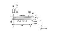
- the second cutting device 16 detects the outer periphery of the display area P4 with a detecting means (detection unit) such as a camera 16a, and the first cutting device 16 along the outer periphery of the display area P4.
- the optical member sheet F1 and the second optical member sheet F2 are cut.
- the third cutting device 19 detects the outer peripheral edge of the display area P4 with a detection means (detection unit) such as a camera 19a, and the third cutting device 19 moves the third optical member sheet F3 along the outer peripheral edge of the display area P4.
- a frame portion G having a predetermined width for arranging a sealant or the like for joining the first substrate P1 and the second substrate P2 is provided. Laser cutting by the second cutting device 16 and the third cutting device 19 is performed within the width of the frame portion G.
- the cut end of the optical member sheet FX may be swollen or wavy due to thermal deformation. For this reason, when the optical member sheet FX after laser cutting is bonded to the optical display component PX, poor bonding such as air mixing and distortion is likely to occur in the optical member sheet FX.
- the cut end of the optical member sheet FX is backed up on the glass surface of the liquid crystal panel P, and the optical member sheet FX It is difficult for the cut ends to bulge, corrugate, and the like, and since it is after bonding to the liquid crystal panel P, the above-mentioned bonding failure is also unlikely to occur.
- the run-out width (tolerance) of the cutting line of the laser processing machine is smaller than that of a cutting blade such as a cutter. Therefore, in this embodiment, compared with the case where the optical member sheet FX is cut using a cutting blade, the width of the frame portion G can be reduced, and the liquid crystal panel P can be reduced in size and / or the display area P4. Larger size is possible. This is effective for application to high-function mobile devices that require expansion of the display screen while the size of the housing is limited, such as smartphones and tablet terminals in recent years.
- the optical member sheet FX is cut into a sheet piece aligned with the display area P4 of the liquid crystal panel P and then bonded to the liquid crystal panel P, the dimensional tolerance of the sheet piece, the dimensional tolerance of the liquid crystal panel P, and the sheet piece and the liquid crystal Since the dimensional tolerance of the relative bonding position with the panel P overlaps, it becomes difficult to narrow the width of the frame part G of the liquid crystal panel P (it becomes difficult to enlarge the display area).
- the optical member sheet FX is bonded to the liquid crystal panel P and then cut in accordance with the display region P4, only the runout tolerance of the cutting line needs to be considered, and the width tolerance of the frame portion G can be reduced. ( ⁇ 0.1 mm or less). Also in this respect, the width of the frame part G of the liquid crystal panel P can be reduced (the display area can be enlarged).
- the cutting force is not input to the liquid crystal panel P, and it becomes difficult for cracks and chips to occur at the edge of the substrate of the liquid crystal panel P, such as a heat cycle.
- the durability against is improved.
- there is no contact with the liquid crystal panel P there is little damage to the electrical component mounting portion P5.
- a laser cut start point pt1 is set on the extension of one long side of the display area P4.
- cutting of this one long side is started from the starting point pt1.
- the end point pt2 of the laser cut is set at a position where the laser goes around the display area P4 and reaches the extension of the short side on the start point side of the display area P4.
- the start point pt1 and the end point pt2 are set so as to be able to withstand the tension when the optical member sheet FX is wound up, leaving a predetermined connection portion in the surplus portion of the optical member sheet FX.
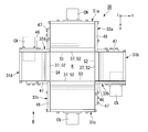
- FIG. 8 is a plan view showing the suction device 30 provided in the second cutting device 16.
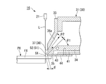
- the second cutting device 16 irradiates the optical member sheet FX with laser light L from the upper side in the orthogonal direction of the optical member sheet FX as shown in FIGS. 12 and 13.
- a laser beam irradiation device 21 for cutting is provided.
- the third cutting device 19 has the same configuration.
- the suction device 30 is disposed on the outer sides of the outer peripheral four sides of an opposing portion (corresponding to the optical member FS, hereinafter referred to as a cutting region (specific region) K) in a rectangular shape in plan view in the optical member sheet FX to be cut.
- the first connection bracket 32a connects the first dust collection box 31a to the side surface of the second dust collection box 31b.
- the second connection bracket 32b connects the second dust collection box 31b to the side surface of the third dust collection box 31c.
- the third connection bracket 32c connects the third dust collection box 31c to the side surface of the fourth dust collection box 31d.
- the fourth connection bracket 32d connects the fourth dust collection box 31d to the side surface of the first dust collection box 31a.
- first to fourth cutting lines processing positions and cutting portions
- the dust collection boxes 31a to 31d, the connecting brackets 32a to 32d, and the cutting lines S1 to S4 may be collectively indicated by reference numerals 31, 32, and SX, respectively.
- the first dust collection box 31a and the third dust collection box 31c are arranged outside the long side portion of the outer periphery of the cutting region K.
- the second dust collection box 31b and the fourth dust collection box 31d are disposed outside the short side portion of the outer periphery of the cutting region K.
- Reference numeral CN in the figure denotes a duct connection pipe projecting from the rear or side of each dust collection box 31.
- each dust collection box 31 has a hollow rectangular parallelepiped shape, and corresponds to a cutting line (processing position, cutting portion) SX side in plan view (hereinafter, the front side of the dust collection box 31). And the front wall 33 located at the cutting line SX.
- Each dust collection box 31 inclines the lower part of the front wall 33 obliquely forward and downward, and forms an extension part 35 having a triangular shape in cross section in the front edge part of the lower wall 34.
- a suction nozzle 36 having a channel 36 a inclined rearwardly upward is formed at the front lower edge part of each dust collection box 31.
- the suction nozzle 36 opens a suction port 37 over the entire width of the dust collection box 31 in the length direction of the corresponding cutting line SX (scanning direction of the laser light L).
- the suction port 37 is disposed close to the corresponding cutting line SX from the outside of the cutting region K.
- the front wall 33 is fixed to the upper wall 38 so that the vertical position can be adjusted.
- the vertical width of the suction port 37 can be adjusted by the vertical movement of the front wall 33.
- the inclination angle (the inclination angle of the inclined surface of the extending portion 35, which is the lower surface of the flow path 36a in FIG. 13) ⁇ 1 in a cross-sectional view of the flow path 36a, is about 45 ° with respect to the upper surface of the optical member sheet FX. .
- the downstream opening angle (opening angle of the upper and lower surfaces of the flow path 36a) ⁇ 2 in the cross-sectional view of the flow path 36a is set to about 15 °.
- Each dust collection box 31 is arranged outside the cutting area K with respect to the corresponding cutting line SX in plan view with a distance d that does not interfere with the laser light L.
- the suction device 30 does not move during laser cutting, and the distance d is smaller than when the suction device 30 moves during laser cutting, which contributes to downsizing of the suction device 30.
- a support air flow path 41 is formed in the lower wall 34 of each dust collection box 31 inside the lower wall 34.
- the flow path 41 feeds support air introduced from, for example, an introduction port 42 that opens to the lower end portion of the rear wall 39 to the outlet port 43 that opens to the lower surface of the extension portion 35.
- a thin plate-shaped guide plate 44 is fixed to the lower surface of the front portion of the lower wall 34.
- a blowing nozzle 51 that opens in front of the lower wall 34 is formed between the guide plate 44 and the lower wall 34.
- the blowout nozzle 51 forms a blowout port 52 that extends across the entire width of the dust collection box 31 just like the suction port 37 just below the suction port 37 of the dust collection box 31.
- each dust collection box 31 is lowered.
- the lower surface of the guide plate 44 is brought into contact with the upper surface of the optical display component PX (the uppermost surface of the optical member sheet FX to be cut), and the suction port 37 is located outside and in the vicinity of the corresponding cutting line SX.
- the blowout port 52 is arrange
- the wind pressure at the tip of the suction nozzle 36 is set to 0.1 kPa or more at static pressure, and the wind speed is set to 7 m / s or more.
- the wind pressure and wind speed at the tip of the blowing nozzle 51 are set smaller than the wind pressure and wind speed of the suction nozzle 36. Therefore, the support air blown out by the blowout nozzle 51 flows from the blowout port 52 so as to return to the suction port 37 side immediately above the blowout port 52 and is sucked into the suction nozzle 36.
- fume attachment to the upper surface of the optical member sheet FX is effectively suppressed in the range of the distance d between the suction port 37 and the cutting line SX.
- the support air blown out by the blow-out nozzle 51 is warm air, and gives heat energy to the fumes that are sublimated materials, making it difficult to adhere to the optical member sheet FX.
- the plurality of cutting lines SX and the plurality of dust collection boxes 31 surround the entire circumference of the rectangular cutting region K in plan view. That is, in the cutting process by the second cutting device 16, the laser beam L scans and cuts the outer periphery of the cutting region K of the optical member sheet FX in an endless manner.
- the cutting in this cutting step is not limited to a rectangular shape, and may be an arbitrary shape. When this shape includes a curve, the suction port 37 and the blowout port 52 can be similarly curved. Moreover, it is not limited to an endless cut, but may be a cut of three sides, two sides, and one side. In this case, the dust collection box 31 may be provided corresponding to only the cutting position.
- each connection bracket 32 includes a side plate 46 fixed to the side surface in the clockwise direction of the corresponding dust collection box 31 and a connection plate 47 fixed to the side surface of the adjacent dust collection box 31. And is formed in an L shape in plan view.
- the connecting plate 47 is formed with a plurality of elongated holes 48 extending in the horizontal direction (the direction along the upper surface of the optical member sheet FX).
- the bolts 49 inserted through the long holes 48 are screwed onto the side surfaces of the adjacent dust collection boxes 31 and tightened. Thereby, adjacent dust collection boxes 31 are connected to each other at a right angle. When the bolts 49 are loosened, the adjacent dust collection boxes 31 can be slid along the long holes 48.
- Each dust collection box 31 moves in a direction along the corresponding cutting line SX by movement along the long hole 48. By this movement, the amount of overlap of the suction port 37 of each dust collection box 31 with respect to the side surface of the adjacent dust collection box 31 is increased or decreased, and thereby the length of the suction port 37 facing the cutting region K is increased or decreased.
- the suction device 30 is formed in a rectangular shape surrounded by the plurality of suction ports 37 by increasing or decreasing the length of the suction ports 37 facing the cutting region K as described above while keeping the plurality of dust collection boxes 31 connected at right angles. Enlarge or reduce the area. Thereby, when performing laser cutting on the optical display component PX having a different size in the cutting region K of the optical member sheet FX, the suction port 37 of each dust collection box 31 is appropriately connected to the cutting line SX of the optical member sheet FX. It becomes possible to make it close to a distance.
- Each dust collection box 31 moves forward and backward in a direction perpendicular to the cutting line SX with respect to the corresponding cutting line SX.
- fumes near the seam between the cutting lines SX can be collected without leakage.
- a plurality of dust collection boxes can be obtained by increasing or decreasing the overlap amount of the suction port 37 with respect to the adjacent dust collection boxes 31 while moving each dust collection box 31 in the direction along the corresponding cutting line SX. 31 is advanced and retracted with respect to the corresponding cutting line SX at the same time. For this reason, the suction port 37 always opens to the corner of the rectangular area, and it becomes possible to collect the fumes without leakage.
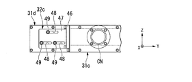
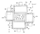
- FIG. 14 and FIG. 15 show a modification of the configuration for moving each dust collection box 31 forward and backward.
- the dust collection boxes 31a to 31d are first to fourth connection brackets 32a ′ to 32d ′ (hereinafter, may be collectively referred to as reference numeral 32 ′) on the side surfaces of the dust collection boxes 31a to 31d that are adjacent in the clockwise direction in the plan view. Connected.
- the first connection bracket 32a ′ connects the first dust collection box 31a to the side surface of the second dust collection box 31b.
- the second connection bracket 32b ′ connects the second dust collection box 31b to the side surface of the third dust collection box 31c.
- connection bracket 32c ′ connects the third dust collection box 31c to the side surface of the fourth dust collection box 31d.
- the fourth connection bracket 32d ′ connects the fourth dust collection box 31d to the side surface of the first dust collection box 31a.
- Each connection bracket 32 ′ connects, for example, a pair of connection plates 47 ′ fixed to the side surface of the corresponding dust collection box 31 in the clockwise direction and the side surface of the adjacent dust collection box 31 in an L shape in plan view. Configured.
- a plurality of long holes 48 are formed in each connecting plate 47 ′, and the bolts 49 inserted through the long holes 48 are screwed into the side surfaces of the corresponding dust collection boxes 31 to be tightened, so that adjacent dust collection boxes 31 are connected to each other. Are concatenated. Further, the dust collection box 31 can be moved forward and backward by sliding the dust collection box 31 with the bolts 49 loosened along the long holes 48. Accordingly, as described above, the plurality of dust collection boxes 31 can be advanced and retracted while being simultaneously moved in the direction along the corresponding cutting line SX. Further, the dust collection box 31 can be advanced and retracted only in the short side direction or the long side direction of the cutting region K.
- the plurality of dust collection boxes 31 are manually moved.
- the plurality of dust collection boxes 31 may be automatically moved by a separate driving device.
- the laser processing apparatus in the embodiment includes the suction device 30 that opens the suction port 37 over the entire length of the cutting line SX in the vicinity of the cutting line SX of the optical member sheet FX in the optical display component PX.
- the suction device 30 that opens the suction port 37 over the entire length of the cutting line SX in the vicinity of the cutting line SX of the optical member sheet FX in the optical display component PX.
- the cutting line SX is provided endlessly on the outer periphery of the cutting region K of the optical member sheet FX, and the suction device 30 is provided so as to surround the entire periphery of the cutting region K. Fume can be sucked and removed without leakage over the entire circumference of the cutting region K. Further, since the suction device 30 can be moved back and forth with respect to the cutting line SX, it can easily cope with laser processing of workpieces having different processing positions.
- the laser processing apparatus includes the blowout port 52 that blows out air toward the product surface between the cutting line SX and the suction port 37, so that the suction device 30 is located between the cutting line SX and the suction port 37. Can prevent fume from adhering to the product surface. Further, the suction device 30 blows warm air from the blowout port, so that fume can be more effectively suppressed from adhering to the product surface between the cutting line SX and the suction port 37.
- the optical member FS having a size corresponding to the display region P4 can be accurately formed on the surface of the liquid crystal panel P, and the frame portion G outside the display region P4 is narrowed to enlarge the display area and downsize the device. Can be achieved.
- disconnection using the laser beam L has a higher precision than the cutting
- the optical member sheet FX (optical member) that remains on the optical display component PX without causing a taper angle (an angle with respect to the direction orthogonal to the bonding surface) due to the inclination of the laser light L to the cut end of the optical member sheet FX.
- the effective area of FS) can be expanded, contributing to further narrowing of the frame. Further, the fumes generated by the laser processing can be sucked without leakage over the entire length of the cutting line SX, and the fume can be prevented from adhering to the product surface, and line contamination due to the fumes adhering to the product can be prevented.
- the present invention is not limited to the above embodiment.
- a configuration in which an optical member sheet is cut into a frame shape is described.
- the present invention is not limited thereto, and for example, at least two optical member sheets are provided.
- the optical member sheet may be divided into slits, cuts penetrating the optical member sheet, or grooves (cuts) having a predetermined depth may be formed in the optical member sheet. Specifically, for example, there are cutting (cutting off), half-cutting, marking processing and the like of the end of the optical member sheet.
- the 2nd cutting device 16 detects the outer periphery of the display area P4 with detection means, such as the camera 16a, and the 1st optical member sheet
- the third cutting device 19 cuts the second optical member sheet F2, and the third cutting device 19 detects the outer peripheral edge of the display area P4 with a detecting means such as a camera 19a, and the third optical device along the outer peripheral edge of the display area P4.
- the member sheet F3 is cut, the configuration of the detection means is not limited to this.
- the film bonding system 1 detects the outer periphery of the bonding surface of the first optical member sheet F1, the second optical member sheet F2, and the liquid crystal panel P in the second bonding sheet F22. It is good also as cutting the cutting line SX set along the outer periphery of the bonding surface.
- the film bonding system 1 has a detection means to detect the outer periphery of the bonding surface of the 3rd optical member sheet
- FIG. 16 is a schematic diagram of first detection means 61 (detection unit) that detects the outer periphery of the bonding surface.
- the 1st detection means 61 with which the film bonding system 1 of this embodiment is provided is the bonding surface (henceforth 1st bonding surface SA1) of liquid crystal panel P and the sheet piece F1S in the 2nd bonding sheet
- Imaging device 63 that captures an image of outer peripheral edge ED
- illumination light source 64 that illuminates outer peripheral edge ED
- a control unit 65 that performs an operation for the purpose.
- Such first detection means 61 is provided on the panel conveyance upstream side of the second cutting device 16 in FIG. 1 and is provided between the pinching roll 15 b and the second cutting device 16.
- the imaging device 63 is fixed and arranged inside the first bonding surface SA1 with respect to the outer peripheral edge ED, and the normal line of the first bonding surface SA1 and the normal line of the imaging surface 63a of the imaging device 63 are arranged.
- the posture is inclined so as to form an angle ⁇ (hereinafter referred to as an inclination angle ⁇ of the imaging device 63).
- the imaging device 63 directs the imaging surface 63a to the outer peripheral edge ED, and captures an image of the outer peripheral edge ED from the side where the sheet piece F1S is bonded in the second bonding sheet F22.
- the inclination angle ⁇ of the imaging device 63 can be set so that the outer peripheral edge of the first substrate P1 constituting the first bonding surface SA1 can be reliably imaged.
- the liquid crystal panel P is formed by so-called multiple chamfering, in which the mother panel is divided into a plurality of liquid crystal panels, the liquid crystal panel P is shifted to the outer peripheral edge of the first substrate P1 and the second substrate P2 constituting the liquid crystal panel P. May occur, and the end surface of the second substrate P2 may be displaced outward from the end surface of the first substrate P1.
- the inclination angle ⁇ of the imaging device 63 can be set so that the outer peripheral edge of the second substrate P2 does not enter the imaging field of view of the imaging device 63.
- the inclination angle ⁇ of the imaging device 63 is a distance H between the first bonding surface SA1 and the center of the imaging surface 63a of the imaging device 63 (hereinafter referred to as the height H of the imaging device 63).
- the height H of the imaging device 63 can be set to fit.
- the inclination angle ⁇ of the imaging device 63 can be set to an angle in the range of 5 ° or more and 20 ° or less.
- the height H of the imaging device 63 and the inclination angle ⁇ of the imaging device 63 can be obtained based on the deviation amount.
- the height H of the imaging device 63 is set to 78 mm
- the inclination angle ⁇ of the imaging device 63 is set to 10 °.
- the inclination angle ⁇ of the imaging device 63 may be 0 °.
- FIG. 17 is a schematic diagram showing a modification of the first detection means 61, and is an example in the case where the inclination angle ⁇ of the imaging device 63 is 0 °.
- each of the imaging device 63 and the illumination light source 64 may be disposed at a position overlapping the outer peripheral edge ED along the normal direction of the first bonding surface SA1.
- a distance H1 between the first bonding surface SA1 and the center of the imaging surface 63a of the imaging device 63 detects the outer peripheral edge ED of the first bonding surface SA1. It can be set at an easy position.
- the height H1 of the imaging device 63 can be set in the range of 50 mm to 150 mm.
- the illumination light source 64 is fixed and arranged on the opposite side to the side where the sheet piece F1S in the second bonding sheet F22 is bonded.
- the illumination light source 64 is arrange
- the optical axis of the illumination light source 64 and the normal line of the imaging surface 63a of the imaging device 63 are parallel.
- the illumination light source 64 may be arrange
- the optical axis of the illumination light source 64 and the normal line of the imaging surface 63a of the imaging device 63 intersect. It may be.
- FIG. 18 is a plan view showing a position where the outer peripheral edge of the bonding surface is detected.
- An inspection area CA is set on the conveyance path of the second bonding sheet F22 shown in the drawing.
- region CA is set in the position corresponding to the outer periphery ED of 1st bonding surface SA1 in liquid crystal panel P conveyed.
- the inspection area CA is set at four locations corresponding to the four corners of the first bonding surface SA1 that is rectangular in plan view, and the corners of the first bonding surface SA1 are detected as the outer peripheral edge ED. It has a configuration.
- the hook-shaped part corresponding to the corner is shown as the outer peripheral edge ED.
- the first detection means 61 in FIG. 16 detects the outer peripheral edge ED in the four inspection areas CA. Specifically, the imaging device 63 and the illumination light source 64 are arranged in each inspection area CA, and the first detection means 61 is provided at each corner of the first bonding surface SA1 for each liquid crystal panel P to be transported. And the outer peripheral edge ED is detected based on the imaging data. Data of the detected outer peripheral edge ED is stored in the control unit 65 shown in FIG.
- region CA may be arrange
- each side (four sides) of the first bonding surface SA1 is detected as an outer peripheral edge.
- the imaging device 63 and the illumination light source 64 are not limited to the configuration arranged in each inspection area CA, but are configured to be able to move along a movement path that is set along the outer peripheral edge ED of the first bonding surface SA1. It may be.
- the imaging device 63 and the illumination light source 64 are configured to detect the outer peripheral edge ED when the imaging device 63 and the illumination light source 64 are positioned in each inspection area CA, so that one imaging device 63 and one illumination light source 64 are provided. In this case, the outer periphery ED can be detected.
- the cutting line for the sheet piece F1S and the second optical member sheet F2 by the second cutting device 16 is set based on the detection result of the outer peripheral edge ED of the first bonding surface SA1.
- the control unit 65 of the first detection means 61 determines that the first optical member F11 is outside the liquid crystal panel P (first bonding surface SA1.
- the cutting line of the sheet piece F1S and the second optical member sheet F2 can be set so as not to protrude outside.
- the setting of the cutting line is not necessarily performed by the control unit 65 of the first detection unit 61, and the data of the outer peripheral edge ED detected by the first detection unit 61 is used, and the calculation of the bonding surface is performed separately.
- a cutting line may be set along the outer peripheral edge.
- the second cutting device 16 cuts the sheet piece F1S and the second optical member sheet F2 at a cutting line set along the outer peripheral edge ED of the bonding surface.
- the second cutting device 16 is provided on the downstream side of the panel conveyance with respect to the first detection means 61.
- the second cutting device 16 includes a portion facing the display region P4 (see FIG. 4) of the sheet piece F1S and the second optical member sheet F2 bonded to the liquid crystal panel P, and a surplus portion outside the facing portion.
- the 2nd single-sided bonding panel P12 in which the 1st optical member F11 and the 2nd optical member F12 were piled up and bonded on the upper surface of liquid crystal panel P is formed.
- the surplus portion is laser-cut along the outer peripheral edge of the liquid crystal panel P at three sides excluding the functional portion in the liquid crystal panel P having a rectangular shape in plan view, and the liquid crystal panel P at one side corresponding to the functional portion. It is possible to adopt a configuration in which the surplus portion is laser-cut at a position that appropriately enters the display region P4 side from the outer peripheral edge.
- the first substrate P1 is a TFT substrate
- FIG. 19 is a schematic diagram of the second detection means 62 (detection unit) that detects the outer peripheral edge of the bonding surface.
- the 2nd detection means 62 with which the film bonding system 1 of this embodiment is provided is the bonding surface (henceforth, 2nd bonding surface SA2) of liquid crystal panel P and the 3rd optical member sheet
- the imaging device 63 that captures an image of the outer peripheral edge ED, the illumination light source 64 that illuminates the outer peripheral edge ED, and the image captured by the imaging device 63 are stored, and the outer peripheral edge ED is based on the image.
- a control unit 65 that performs a calculation for detecting.
- the second detection means 62 has the same configuration as the first detection means 61 described above.
- Such second detection means 62 is provided on the panel conveyance upstream side of the third cutting device 19 in FIG. 1 and is provided between the pinching roll 18b and the third cutting device 19.
- the 2nd detection means 62 detects outer periphery ED of 2nd bonding surface SA2 similarly to the above-mentioned 1st detection means 61 in the test
- the cutting line for the third optical member sheet F3 by the third cutting device 19 is set based on the detection result of the outer peripheral edge ED of the second bonding surface SA2.
- the control unit 65 of the second detection means 62 causes the third optical member F13 to be outside the liquid crystal panel P (second bonding surface SA2).
- the cutting line of the third optical member sheet F3 can be set so that the size does not protrude outside.
- the setting of the cutting line is not necessarily performed by the control unit 65 of the second detection unit 62, and the data of the outer peripheral edge ED detected by the second detection unit 62 is used, and the bonding surface is separately calculated using a calculation unit.
- a cutting line may be set along the outer peripheral edge.
- the third cutting device 19 cuts the third optical member sheet F3 at the cutting line set along the outer peripheral edge ED of the bonding surface.
- the third cutting device 19 detects a portion facing the display region P4 (see FIG. 6) of the third optical member sheet F3 bonded to the liquid crystal panel P and a surplus portion outside the facing portion.
- the third optical member F13 (see FIG. 7) having a size corresponding to the display area P4 is cut out along the cutting line set based on the outer peripheral edge ED.
- the double-sided bonding panel P13 by which the 3rd optical member F13 was bonded by the upper surface of the 2nd single-sided bonding panel P12 is formed.
- fume adhesion to the product surface can be effectively suppressed without affecting the product processing accuracy, which can contribute to narrowing the frame.
- the outer periphery of the bonding surface is detected for every some liquid crystal panel P using a detection means (detection part), and each liquid crystal panel P based on the detected outer periphery.
- the cutting position of the sheet piece F1S, the second optical member sheet F2, and the third optical member sheet F3 bonded to each other is set.
Landscapes
- Engineering & Computer Science (AREA)
- Physics & Mathematics (AREA)
- Optics & Photonics (AREA)
- Plasma & Fusion (AREA)
- Mechanical Engineering (AREA)
- Laser Beam Processing (AREA)
- Liquid Crystal (AREA)
- Devices For Indicating Variable Information By Combining Individual Elements (AREA)
- Nonlinear Science (AREA)
- Manufacturing & Machinery (AREA)
- Chemical & Material Sciences (AREA)
- Crystallography & Structural Chemistry (AREA)
- General Physics & Mathematics (AREA)
Abstract
Priority Applications (2)
| Application Number | Priority Date | Filing Date | Title |
|---|---|---|---|
| KR1020157027044A KR20150140664A (ko) | 2013-04-08 | 2014-01-27 | 레이저 가공 장치 및 광학 표시 디바이스의 생산 시스템 |
| CN201480018797.6A CN105102175A (zh) | 2013-04-08 | 2014-01-27 | 激光加工装置以及光学显示器件的生产系统 |
Applications Claiming Priority (4)
| Application Number | Priority Date | Filing Date | Title |
|---|---|---|---|
| JP2013080846 | 2013-04-08 | ||
| JP2013-080846 | 2013-04-08 | ||
| JP2013-104400 | 2013-05-16 | ||
| JP2013104400A JP6120161B2 (ja) | 2013-04-08 | 2013-05-16 | レーザー加工装置及び光学表示デバイスの生産システム |
Publications (1)
| Publication Number | Publication Date |
|---|---|
| WO2014167875A1 true WO2014167875A1 (fr) | 2014-10-16 |
Family
ID=51689293
Family Applications (1)
| Application Number | Title | Priority Date | Filing Date |
|---|---|---|---|
| PCT/JP2014/051682 Ceased WO2014167875A1 (fr) | 2013-04-08 | 2014-01-27 | Dispositif d'usinage laser et système de production de dispositif d'affichage optique |
Country Status (5)
| Country | Link |
|---|---|
| JP (1) | JP6120161B2 (fr) |
| KR (1) | KR20150140664A (fr) |
| CN (1) | CN105102175A (fr) |
| TW (1) | TW201446381A (fr) |
| WO (1) | WO2014167875A1 (fr) |
Cited By (1)
| Publication number | Priority date | Publication date | Assignee | Title |
|---|---|---|---|---|
| US20210181397A1 (en) * | 2017-04-28 | 2021-06-17 | Samsung Display Co., Ltd. | Polarizing layer, display device with the same, and fabricating method for the display device |
Families Citing this family (2)
| Publication number | Priority date | Publication date | Assignee | Title |
|---|---|---|---|---|
| JP6998158B2 (ja) * | 2017-09-07 | 2022-01-18 | 株式会社ディスコ | 切削ブレード供給装置 |
| KR102241016B1 (ko) * | 2020-01-30 | 2021-04-28 | 주식회사 제이스텍 | 디스플레이 레이저 컷팅설비 인스펙션 공정방법 |
Citations (10)
| Publication number | Priority date | Publication date | Assignee | Title |
|---|---|---|---|---|
| JPH0417361U (fr) * | 1990-05-26 | 1992-02-13 | ||
| JP2003107452A (ja) * | 2001-09-17 | 2003-04-09 | Internatl Business Mach Corp <Ibm> | 液晶表示パネルの製造方法、液晶表示装置の製造方法、および、液晶表示装置の製造装置 |
| JP2005074910A (ja) * | 2003-09-02 | 2005-03-24 | Fuji Photo Film Co Ltd | カラープリンタ |
| WO2008143042A1 (fr) * | 2007-05-16 | 2008-11-27 | Nitto Denko Corporation | Procédé de traitement au laser et produit traité au laser |
| JP2009061498A (ja) * | 2006-10-17 | 2009-03-26 | Nitto Denko Corp | 光学部材貼合せ方法およびそれを用いた装置 |
| US20090223944A1 (en) * | 2008-03-04 | 2009-09-10 | Universal Laser Systems, Inc. | Laser-Based Material Processing Exhaust Systems and Methods for Using Such Systems |
| WO2009128207A1 (fr) * | 2008-04-15 | 2009-10-22 | 日東電工株式会社 | Procédé et appareillage pour la fabrication continue d'un élément d'affichage à cristaux liquides |
| JP2010167484A (ja) * | 2009-01-26 | 2010-08-05 | Takei Electric Industries Co Ltd | 薄膜積層ガラス基板の薄膜除去方法及び装置 |
| WO2011004509A1 (fr) * | 2009-07-07 | 2011-01-13 | 株式会社片岡製作所 | Machine de découpe par laser |
| JP2013152456A (ja) * | 2011-12-27 | 2013-08-08 | Sumitomo Chemical Co Ltd | レーザー光照射装置、光学部材貼合体の製造装置、レーザー光照射方法及び光学部材貼合体の製造方法 |
Family Cites Families (4)
| Publication number | Priority date | Publication date | Assignee | Title |
|---|---|---|---|---|
| JPH04361103A (ja) | 1991-06-06 | 1992-12-14 | Olympus Optical Co Ltd | 相対位置検出方法及び装置 |
| KR20040002796A (ko) * | 2002-06-28 | 2004-01-07 | 후지 샤신 필름 가부시기가이샤 | 편광판 점착방법 및 그 장치 |
| KR100848854B1 (ko) * | 2008-04-21 | 2008-07-30 | 주식회사 탑 엔지니어링 | 취성기판의 스크라이빙 장치 및 그 방법 |
| JP2011178636A (ja) * | 2010-03-03 | 2011-09-15 | Mitsuboshi Diamond Industrial Co Ltd | 脆性材料基板の分断方法及び脆性材料部材 |
-
2013
- 2013-05-16 JP JP2013104400A patent/JP6120161B2/ja active Active
-
2014
- 2014-01-27 WO PCT/JP2014/051682 patent/WO2014167875A1/fr not_active Ceased
- 2014-01-27 KR KR1020157027044A patent/KR20150140664A/ko not_active Withdrawn
- 2014-01-27 CN CN201480018797.6A patent/CN105102175A/zh active Pending
- 2014-04-08 TW TW103112909A patent/TW201446381A/zh unknown
Patent Citations (10)
| Publication number | Priority date | Publication date | Assignee | Title |
|---|---|---|---|---|
| JPH0417361U (fr) * | 1990-05-26 | 1992-02-13 | ||
| JP2003107452A (ja) * | 2001-09-17 | 2003-04-09 | Internatl Business Mach Corp <Ibm> | 液晶表示パネルの製造方法、液晶表示装置の製造方法、および、液晶表示装置の製造装置 |
| JP2005074910A (ja) * | 2003-09-02 | 2005-03-24 | Fuji Photo Film Co Ltd | カラープリンタ |
| JP2009061498A (ja) * | 2006-10-17 | 2009-03-26 | Nitto Denko Corp | 光学部材貼合せ方法およびそれを用いた装置 |
| WO2008143042A1 (fr) * | 2007-05-16 | 2008-11-27 | Nitto Denko Corporation | Procédé de traitement au laser et produit traité au laser |
| US20090223944A1 (en) * | 2008-03-04 | 2009-09-10 | Universal Laser Systems, Inc. | Laser-Based Material Processing Exhaust Systems and Methods for Using Such Systems |
| WO2009128207A1 (fr) * | 2008-04-15 | 2009-10-22 | 日東電工株式会社 | Procédé et appareillage pour la fabrication continue d'un élément d'affichage à cristaux liquides |
| JP2010167484A (ja) * | 2009-01-26 | 2010-08-05 | Takei Electric Industries Co Ltd | 薄膜積層ガラス基板の薄膜除去方法及び装置 |
| WO2011004509A1 (fr) * | 2009-07-07 | 2011-01-13 | 株式会社片岡製作所 | Machine de découpe par laser |
| JP2013152456A (ja) * | 2011-12-27 | 2013-08-08 | Sumitomo Chemical Co Ltd | レーザー光照射装置、光学部材貼合体の製造装置、レーザー光照射方法及び光学部材貼合体の製造方法 |
Cited By (2)
| Publication number | Priority date | Publication date | Assignee | Title |
|---|---|---|---|---|
| US20210181397A1 (en) * | 2017-04-28 | 2021-06-17 | Samsung Display Co., Ltd. | Polarizing layer, display device with the same, and fabricating method for the display device |
| US12153237B2 (en) * | 2017-04-28 | 2024-11-26 | Samsung Display Co., Ltd. | Fabricating method for a display device with polarizing layer |
Also Published As
| Publication number | Publication date |
|---|---|
| CN105102175A (zh) | 2015-11-25 |
| TW201446381A (zh) | 2014-12-16 |
| JP2014217879A (ja) | 2014-11-20 |
| KR20150140664A (ko) | 2015-12-16 |
| JP6120161B2 (ja) | 2017-04-26 |
Similar Documents
| Publication | Publication Date | Title |
|---|---|---|
| JP5791018B2 (ja) | 光学表示デバイスの生産システム及び生産方法 | |
| KR101973832B1 (ko) | 광학 표시 디바이스의 생산 시스템 및 광학 표시 디바이스의 생산 방법 | |
| KR101572402B1 (ko) | 레이저 광 조사 장치, 광학 부재 접합체의 제조 장치, 레이저 광 조사 방법 및 광학 부재 접합체의 제조 방법 | |
| TWI441703B (zh) | 光學組件貼合體之製造系統、製造方法及記錄媒體 | |
| KR20160009561A (ko) | 광학 표시 디바이스의 생산 시스템 | |
| KR20150121004A (ko) | 광학 표시 디바이스의 생산 시스템 | |
| JP6120161B2 (ja) | レーザー加工装置及び光学表示デバイスの生産システム | |
| KR20150048757A (ko) | 광학 부재 접합체의 제조 장치 | |
| KR20160009556A (ko) | 광학 표시 디바이스의 생산 시스템 및 광학 표시 디바이스의 생산 방법 | |
| WO2014024803A1 (fr) | Système et procédé de production de dispositif d'affichage optique | |
| WO2013081040A1 (fr) | Dispositif et procédé pour fabriquer un article collé à élément optique | |
| JP5828961B2 (ja) | 光学表示デバイスの生産方法および光学表示デバイスの生産システム | |
| JP2015049115A (ja) | 光学部材貼合体の製造方法 | |
| JP5924726B2 (ja) | 光学部材貼合体の製造装置及び製造方法 | |
| JP6227279B2 (ja) | 光学部材貼合体の製造装置及び製造方法 | |
| WO2015030066A1 (fr) | Procédé de production d'un élément optique stratifié | |
| JP5724146B2 (ja) | 光学部材貼合体の製造システム、製造方法及び記録媒体 | |
| WO2014024872A1 (fr) | Procédé et système de production d'un dispositif optique d'affichage | |
| JP2014224912A (ja) | 光学表示デバイスの生産システム及び生産方法 | |
| WO2014185092A1 (fr) | Système de fabrication d'organe optique soudé, procédé de fabrication et support d'enregistrement | |
| JP2015049348A (ja) | 光学部材貼合体の製造方法 |
Legal Events
| Date | Code | Title | Description |
|---|---|---|---|
| WWE | Wipo information: entry into national phase |
Ref document number: 201480018797.6 Country of ref document: CN |
|
| 121 | Ep: the epo has been informed by wipo that ep was designated in this application |
Ref document number: 14782994 Country of ref document: EP Kind code of ref document: A1 |
|
| ENP | Entry into the national phase |
Ref document number: 20157027044 Country of ref document: KR Kind code of ref document: A |
|
| NENP | Non-entry into the national phase |
Ref country code: DE |
|
| 122 | Ep: pct application non-entry in european phase |
Ref document number: 14782994 Country of ref document: EP Kind code of ref document: A1 |