WO2014171214A1 - Procédé de gravure - Google Patents
Procédé de gravure Download PDFInfo
- Publication number
- WO2014171214A1 WO2014171214A1 PCT/JP2014/055614 JP2014055614W WO2014171214A1 WO 2014171214 A1 WO2014171214 A1 WO 2014171214A1 JP 2014055614 W JP2014055614 W JP 2014055614W WO 2014171214 A1 WO2014171214 A1 WO 2014171214A1
- Authority
- WO
- WIPO (PCT)
- Prior art keywords
- gas
- etching
- chamber
- film
- etching method
- Prior art date
- Legal status (The legal status is an assumption and is not a legal conclusion. Google has not performed a legal analysis and makes no representation as to the accuracy of the status listed.)
- Ceased
Links
Images


Classifications
-
- H—ELECTRICITY
- H10—SEMICONDUCTOR DEVICES; ELECTRIC SOLID-STATE DEVICES NOT OTHERWISE PROVIDED FOR
- H10P—GENERIC PROCESSES OR APPARATUS FOR THE MANUFACTURE OR TREATMENT OF DEVICES COVERED BY CLASS H10
- H10P50/00—Etching of wafers, substrates or parts of devices
- H10P50/20—Dry etching; Plasma etching; Reactive-ion etching
- H10P50/28—Dry etching; Plasma etching; Reactive-ion etching of insulating materials
- H10P50/282—Dry etching; Plasma etching; Reactive-ion etching of insulating materials of inorganic materials
- H10P50/283—Dry etching; Plasma etching; Reactive-ion etching of insulating materials of inorganic materials by chemical means
Definitions
- the present invention relates to an etching method for etching a film of a predetermined material formed on a substrate.
- Patent Documents 1 and 2 When etching silicon oxide (SiO 2 ) as an oxide, hydrogen fluoride (HF) gas alone or a mixed gas of HF gas and ammonia (NH 3 ) gas is used.
- HF hydrogen fluoride
- NH 3 ammonia
- COR is a technique for etching an oxide, but since it is a low-damage etching technique that performs etching without generating plasma in the chamber, this technique has recently been applied to etching a silicon nitride (SiN) film. It is being considered.
- etching gas for etching the SiN film without generating plasma in the chamber HF gas + F 2 gas has been studied (for example, Patent Document 3).
- the SiN film is often adjacent to Si such as a polysilicon (poly-Si) film or Si substrate, or an SiO 2 film.
- the SiN film is converted into HF gas and F
- the SiO 2 film is etched by NH 3 gas and HF gas generated as reaction products at a low temperature, and poly-Si is etched at a high temperature. Therefore, there is a problem that it is difficult to etch the SiN film with a high selection ratio with respect to the SiO 2 film and the poly-Si film.
- an object of the present invention is to provide an etching method capable of etching a silicon nitride film with a high selectivity with respect to a silicon oxide film and / or a polysilicon film by a technique that does not generate plasma in the chamber. is there.
- a substrate to be processed having a silicon nitride film on the surface and having a polysilicon film and / or a silicon oxide film provided adjacent to the silicon nitride film is placed in the chamber. And supplying the F-containing gas and the O 2 gas into the chamber in a state where at least the O 2 gas is excited, and by using these gases, the silicon nitride film and the polysilicon film and / or An etching method comprising selectively etching the silicon oxide film is provided.
- etching may be performed by further supplying an inert gas.
- an inert gas In this case, N 2 gas and / or Ar gas can be suitably used as the inert gas.
- the F-containing gas and the O 2 gas may be introduced into the chamber after being collectively excited by plasma outside the chamber, or the F-containing gas and The O 2 gas may be separately excited outside the chamber by plasma and separately introduced into the chamber, or the F-containing gas may be introduced into the chamber without being excited, The O 2 gas may be introduced into the chamber after being excited by plasma outside the chamber.
- oxygen plasma may be supplied to the substrate to be processed to pre-oxidize the surface of the substrate to be processed.
- F 2 gas diluted with an inert gas can be used as the F-containing gas.
- the inert gas N 2 gas and / or Ar gas can be suitably used.
- the volume ratio of F 2 gas and O 2 gas can be in the range of 1: 2 to 1: 1000.
- a ClF 3 gas can also be used as the F-containing gas.
- the volume ratio of ClF 3 gas and O 2 gas can be in the range of 1: 4 to 1: 1000.
- the temperature of the mounting table on which the substrate to be processed is mounted in the chamber can be set to a range of 10 to 200 ° C.
- the pressure in the chamber can be set to a range of 13 to 1333 Pa.
- a storage medium that operates on a computer and stores a program for controlling an etching apparatus.
- a storage medium is provided for allowing a computer to control the etching apparatus so that the etching method can be performed.
- the SiN film on the surface of the substrate without generating a plasma in the chamber, SiO 2 film and / or poly-Si to a high etching rate, and provided adjacent to the SiN film It can be etched with high selectivity to the film.
- FIG. 1 It is a schematic block diagram which shows an example of the processing system carrying the etching apparatus used in order to implement the etching method which concerns on embodiment of this invention. It is sectional drawing which shows schematic structure of an example of the etching apparatus mounted in the processing system of FIG. It is sectional drawing which shows schematic structure of the other example of the etching apparatus mounted in the processing system of FIG. It is sectional drawing which shows schematic structure of the further another example of the etching apparatus mounted in the processing system of FIG. It is a schematic block diagram which shows the other example of the processing system carrying the etching apparatus used in order to implement the etching method which concerns on embodiment of this invention. It is sectional drawing which shows the heat processing apparatus mounted in the processing system of FIG.
- the flow ratio of O 2 gas to the F 2 gas (O 2 / F 2), SiN film, poly-Si film, SiO 2 film It is a figure which shows the relationship with the etching amount.
- the F 2 gas diluted with N 2 gas as the F-containing gas is a diagram showing the temperature of the mounting table, SiN film, poly-Si film, the relation between the etching amount of the SiO 2 film.
- the F-containing gas as F 2 gas diluted with N 2 gas a diagram illustrating the chamber pressure, SiN film, poly-Si film, the relation between the etching amount of the SiO 2 film.
- FIG. 1 In the case of using a ClF 3 gas as F-containing gas is a diagram showing the temperature of the mounting table, SiN film, poly-Si film, the relation between the etching amount of the SiO 2 film.
- a ClF 3 gas as F-containing gas In the case of using a ClF 3 gas as F-containing gas is a diagram showing the pressure inside the chamber, SiN film, poly-Si film, the relation between the etching amount of the SiO 2 film.
- F-containing gas is a diagram showing the conditions of the pre-oxidation treatment, the etching amount of the SiN film, and a relationship between the etching selectivity of the SiN film to polysilicon and SiO 2 film.
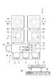
- FIG. 1 is a schematic configuration diagram showing an example of a processing system equipped with an etching apparatus for carrying out the etching method of the present invention.
- the processing system 1 includes a loading / unloading section 2 for loading / unloading a semiconductor wafer (hereinafter simply referred to as a wafer) W, and two load lock chambers (L / L) 3 provided adjacent to the loading / unloading section 2. And an etching apparatus 5 provided adjacent to each load lock chamber 3 for performing etching on the wafer W without generating plasma.
- the loading / unloading unit 2 has a transfer chamber (L / M) 12 in which a first wafer transfer mechanism 11 for transferring the wafer W is provided.
- the first wafer transfer mechanism 11 has two transfer arms 11a and 11b that hold the wafer W substantially horizontally.
- a mounting table 13 is provided on the side of the transfer chamber 12 in the longitudinal direction. For example, three carriers C capable of accommodating a plurality of wafers W arranged side by side can be connected to the mounting table 13. .
- an orienter 14 is installed adjacent to the transfer chamber 12 to rotate the wafer W and optically determine the amount of eccentricity.
- the wafer W is held by the transfer arms 11 a and 11 b, and is moved to a desired position by moving straight and moving up and down substantially in a horizontal plane by driving the first wafer transfer mechanism 11.
- the transfer arms 11a and 11b are moved forward and backward with respect to the carrier C, the orienter 14 and the load lock chamber 3 on the mounting table 13, respectively.
- Each load lock chamber 3 is connected to the transfer chamber 12 with a gate valve 16 interposed between the load lock chamber 3 and the transfer chamber 12, respectively.
- a second wafer transfer mechanism 17 for transferring the wafer W is provided in each load lock chamber 3.
- the load lock chamber 3 is configured to be evacuated to a predetermined degree of vacuum.
- the second wafer transfer mechanism 17 has a pick that holds the wafer W substantially horizontally. In the second wafer transfer mechanism 17, it is possible to move the pick between the load lock chamber 3 and the etching apparatus 5, and thereby the wafer W is moved between the load lock chamber 3 and the etching apparatus 5. It is possible to transport with.
- the processing system 1 has a control unit 90.
- the control unit 90 includes a process controller 91 including a microprocessor (computer) that controls each component of the processing system 1.
- a user interface 92 Connected to the process controller 91 is a user interface 92 having a keyboard for an operator to input commands and the like for managing the processing system 1 and a display for visualizing and displaying the operating status of the processing system 1.
- the process controller 91 also includes a control program and a process for realizing various processes executed by the processing system 1, for example, supply of process gas in the etching apparatus 5 described later, exhaust in the chamber, and the like by controlling the process controller.
- a processing unit that is a control program for causing each component of the processing system 1 to execute a predetermined process according to conditions, and a storage unit 93 that stores various databases and the like are connected.
- the recipe is stored in an appropriate storage medium (not shown) in the storage unit 93. If necessary, an arbitrary recipe is called from the storage unit 93 and is executed by the process controller 91, whereby a desired process in the processing system 1 is performed under the control of the process controller 91.
- a wafer W having a SiN film to be etched on the surface and at least one of a SiO 2 film and a poly-Si film formed adjacent thereto is used.
- a plurality of such wafers W are stored in the carrier C, and the carrier C is mounted on the loading / unloading unit 2 of the processing system 1.
- a single wafer W is loaded from the carrier C of the loading / unloading unit 2 by one of the transfer arms 11 a and 11 b of the first wafer transfer mechanism 11 with the atmosphere side gate valve 16 opened.
- the gate valve 16 on the atmosphere side is closed and the load lock chamber 3 is evacuated, then the gate valve 54 is opened, the pick is extended to the etching apparatus 5, and the wafer W is transferred to the etching apparatus 5.
- the pick is returned to the load lock chamber 3, the gate valve 54 is closed, and an etching process is performed in the etching apparatus 5.
- the gate valve 54 is opened, and the wafer W after the etching process on the mounting table 42 is retracted to the load lock chamber 3 by the pick of the second wafer transfer mechanism 17 to transfer the first wafer.
- the carrier 11 is returned to the carrier C by one of the transport arms 11 a and 11 b of the mechanism 11. Thereby, processing of one wafer is completed.
- FIG. 2 is a cross-sectional view showing an example of the etching apparatus 5.
- the etching apparatus 5 includes a sealed chamber 40, and a mounting table 42 on which the wafer W is mounted in a substantially horizontal state is provided inside the chamber 40.
- the etching apparatus 5 also includes a gas supply mechanism 43 that supplies F-containing gas, O 2 gas, and the like to the chamber 40, and an exhaust mechanism 44 that exhausts the interior of the chamber 40.
- the chamber 40 includes a chamber body 51 and a lid 52.
- the chamber body 51 has a substantially cylindrical side wall portion 51 a and a bottom portion 51 b, and an upper portion is an opening, and the opening is closed by a lid portion 52.
- the side wall 51a and the lid 52 are sealed by a sealing member (not shown), and the airtightness in the chamber 40 is ensured.
- a gas introduction nozzle 61 is inserted into the top wall of the lid 52 from the upper side into the chamber 40.
- a loading / unloading port 53 for loading / unloading the wafer W into / from the load lock chamber 3 is provided in the side wall 51a, and the loading / unloading port 53 can be opened and closed by a gate valve 54.
- the mounting table 42 has a substantially circular shape in plan view, and is fixed to the bottom 51 b of the chamber 40.
- a temperature controller 55 that adjusts the temperature of the mounting table 42 is provided inside the mounting table 42.
- the temperature controller 55 includes, for example, a pipe line through which a temperature adjusting medium (for example, water) circulates, and heat exchange is performed with the temperature adjusting medium flowing in the pipe line, thereby the mounting table 42.
- the temperature of the wafer W on the mounting table 42 is controlled.
- the gas supply mechanism 43 has a first gas supply pipe 62 connected to the gas introduction nozzle 61 described above, and a gas exciter 63 that excites gas by plasma is connected to the first gas supply pipe 62. Has been.
- a second gas supply pipe 64 and a third gas supply pipe 65 are connected to the gas excitation unit 63.
- An F-containing gas supply source 66 is connected to the second gas supply pipe 64, and an O 2 gas supply source 67 is connected to the third gas supply pipe 65.
- the first gas supply pipe 62, the fourth of the gas supply pipe 68 is connected to the fourth gas supply pipe 68, N 2 gas supply source 69 for supplying N 2 gas is connected .
- the F-containing gas supply source 66 supplies a gas containing fluorine (F), and examples of the F-containing gas include highly reactive gases such as F 2 gas or ClF 3 gas.
- the F-containing gas is F 2 gas
- the F-containing gas is ClF 3 gas
- the second to fourth gas supply pipes 64, 65 and 68 are provided with a flow rate controller 80 for opening and closing the flow path and controlling the flow rate.
- the flow rate controller 80 is constituted by, for example, an on-off valve and a mass flow controller.
- the gas supply mechanism 43 having such a configuration has been supplied from the F-containing gas supply source 66, O 2 gas supplied from the F-containing gas and O 2 gas supply source 67, excited by plasma gas excitation portion 63
- the excited gas is further diluted with N 2 gas from the N 2 gas supply source 69 as necessary, and is introduced into the chamber 40 through the first gas supply pipe 62 and the gas introduction nozzle 61. Is done.
- N 2 gas from the N 2 gas supply source 69 may also be used as the purge gas.
- the F-containing gas supplied from the F-containing gas supply source 66 is F 2 gas
- other than N 2 gas may be used as an inert gas for diluting the F 2 gas
- an inert gas other than N 2 gas Ar gas can be preferably used.
- another inert gas supply source may be provided instead of the N 2 gas supply source 69, and Ar gas can be suitably used as the other inert gas. That is, the gas supplied from the gas supply mechanism 43 during the etching process is an F-containing gas and an O 2 gas.
- the F-containing gas is an F 2 gas
- an inert gas is supplied in addition thereto. .
- N 2 gas and / or Ar gas is suitable as the inert gas.
- the F-containing gas is ClF 3 gas
- the inert gas is supplied as necessary.
- the configuration of the gas excitation unit 63 is not particularly limited as long as the gas can be excited by plasma.
- the gas may be excited at a position adjacent to the chamber 40, and the gas excited from a hole formed in the wall that partitions the chamber 40, for example, a ceiling wall, may be introduced into the chamber 40.
- the exhaust mechanism 44 has an exhaust pipe 82 connected to an exhaust port 81 formed in the bottom 51 b of the chamber 40, and further, an automatic pressure provided in the exhaust pipe 82 for controlling the pressure in the chamber 40.
- a control valve (APC) 83 and a vacuum pump 84 for evacuating the chamber 40 are provided.
- Two capacitance manometers 86a and 86b as pressure gauges for measuring the pressure in the chamber 40 are provided from the side wall of the chamber 40 into the chamber 40.
- the capacitance manometer 86a is for high pressure
- the capacitance manometer 86b is for low pressure.
- a temperature sensor (not shown) for detecting the temperature of the wafer W is provided in the vicinity of the wafer W mounted on the mounting table 42.
- Al is used as the material of various components such as the chamber 40 and the mounting table 42 that constitute the etching apparatus 5.
- the Al material constituting the chamber 40 may be a solid material, or may be an inner surface (such as the inner surface of the chamber body 51) subjected to an anodizing treatment.
- the surface of Al constituting the mounting table 42 is required to have wear resistance, it is preferable to perform anodization to form an oxide film (Al 2 O 3 ) having high wear resistance on the surface.
- the wafer W having the above-described configuration is loaded into the chamber 40 from the loading / unloading port 53 by the pick of the second wafer transfer mechanism 17 in the load lock chamber 3, and placed on the mounting table 42. Place.
- pre-oxidation treatment with oxygen plasma is performed as necessary.
- the temperature of the mounting table 42 by the temperature controller 55 is adjusted to a predetermined temperature, the O 2 gas from the O 2 gas supply source 67 for the gas supply mechanism 43 into plasma by exciting a gas pumping unit 63
- the generated oxygen plasma is introduced into the chamber 40 through the first gas supply pipe 62 and the gas introduction nozzle 61.
- the O 2 plasma pre-oxidation treatment by is formed of SiO 2 on the surface of the polysilicon film to protect from the etching, it is to easily etched by the surface of the SiN film is oxidized (SiNO formation).
- SiNO formation oxidized
- the pressure in the chamber 40 is preferably in the range of 13 to 1333 Pa (0.1 to 10 Torr), and the temperature of the mounting table 42 is preferably in the range of 10 to 200 ° C. Further, although the effect becomes higher as the processing time becomes longer, 180 sec or less is preferable from the viewpoint of throughput.
- this pretreatment may be performed in a separate chamber instead of the chamber 40 of the etching apparatus 5.
- F-containing gas and O 2 gas are introduced into the chamber 40 while being excited by plasma, and the SiN film is selectively etched.
- the temperature of the mounting table 42 is adjusted to a predetermined range by the temperature controller 55, and the pressure in the chamber 40 is adjusted to the predetermined range, so that the F-containing gas supply source 66 of the gas supply mechanism 43 can be adjusted.
- a fixed amount of F-containing gas is supplied to the gas excitation unit 63 via the second gas supply pipe 64, and a predetermined amount of O 2 gas is gas-excited from the O 2 gas supply source 67 via the third gas supply pipe 65.
- the ratio of the F-containing gas and the O 2 gas supplied to the unit 63 and supplied to the gas excitation unit 63 is set to a predetermined ratio. Then, these are excited by plasma in the gas excitation unit 63, the excited gas is diluted with N 2 gas as necessary, and the inside of the chamber 40 is passed through the first gas supply pipe 62 and the gas introduction nozzle 61. Then, the SiN film is etched.
- N 2 gas instead of N 2 gas, other inert gas such as Ar gas may be used.
- the excited F-containing gas and O 2 gas act on the SiN film, and the SiN film can be etched at a high etching rate.
- the etching rate of the poly-Si film and the SiO 2 film by the F-containing gas and the O 2 gas can be lowered, and the SiN film can be etched with a high selectivity with respect to these films.
- a SiO 2 film is used as a base, it is possible to perform etching without damaging the SiO 2 film such as roughness.
- F 2 gas or ClF 3 gas can be suitably used.
- the F-containing gas is F 2 gas
- the pressure in the chamber 40 is preferably in the range of 13 to 1333 Pa (0.1 to 10 Torr). More preferably, it is 66 to 666 Pa (0.5 to 5 Torr), and more preferably 133 to 333 Pa (1 to 2.5 Torr).
- the temperature of the mounting table 42 (substantially the temperature of the wafer) is preferably low, and good characteristics can be obtained at a temperature of 35 ° C. or lower, for example. However, if the temperature exceeds 200 ° C., the etching characteristics deteriorate. Therefore, the temperature of the mounting table 42 is preferably in the range of 10 to 200 ° C. More preferably, it is 10 to 100 ° C, and more preferably 15 to 55 ° C.
- the volume ratio of F 2 gas and O 2 gas may be in the range of 1: 2 to 1: 1000. preferable. More preferably, it is in the range of 1: 4 to 1: 200.
- the gas flow rate varies greatly depending on the substrate to be processed, but the total of F 2 gas and O 2 gas is preferably 100 to 5000 mL / min (sccm), and the inert gas is preferably 10 to 2000 mL / min (sccm).
- the volume ratio of ClF 3 gas to O 2 gas is preferably in the range of 1: 4 to 1: 1000. More preferably, it is in the range of 1:10 to 1: 300.
- the gas flow rate varies greatly depending on the substrate to be processed, but the total of ClF 3 gas and O 2 gas is preferably 100 to 5000 mL / min (sccm). When an inert gas is introduced, 10 to 2000 mL / min (sccm) is preferable.
- the etching rate of the SiN film is 8 nm / min or more, and the etching selection for the poly-Si film and the SiO 2 film is selected.
- the ratio can be 40 or more.
- the gate valve 54 is opened, and the wafer W after the etching process on the mounting table 42 is unloaded from the chamber 40 by the pick of the second wafer transfer mechanism 17 and etched. Etching by the apparatus 5 is finished.
- pre-oxidation treatment is an optional treatment performed as necessary, but the effect is particularly great when the F-containing gas is ClF 3 gas.
- the etching apparatus may have a structure as shown in FIG. 3 or a structure shown in FIG.
- FIG. 3 an example in which F-containing gas and O 2 gas are separately excited is shown.
- a first gas introduction nozzle 61 a and a second gas introduction nozzle 61 b are inserted into the chamber 40 from above from the top wall of the lid portion 52 of the chamber 40.
- the gas supply mechanism 43 includes a first gas supply pipe 62a and a second gas supply pipe 62b connected to the first gas introduction nozzle 61a and the second gas introduction nozzle 61b, respectively.
- a first gas excitation part 63a is connected to the first gas supply line 62a
- a second gas excitation part 63b is connected to the second gas supply line 62b.
- gas excitation parts excite gas by plasma like the gas excitation part 63 of the first example.
- a third gas supply pipe 71 is connected to the first gas excitation section 63a, and an F-containing gas supply source 66 is connected to the third gas supply pipe 71.
- a fourth gas supply pipe 72 is connected to the second gas excitation section 63 b, and an O 2 gas supply source 67 is connected to the fourth gas supply pipe 72.
- a fifth gas supply pipe 68a is connected to the first gas supply pipe 62a, and a first N 2 gas supply source 69a for supplying N 2 gas is connected to the fifth gas supply pipe 68a. It is connected.
- a sixth gas supply pipe 68b is connected to the second gas supply pipe 62b, and a second N 2 gas supply source 69b for supplying N 2 gas is connected to the sixth gas supply pipe 68b. It is connected.
- the third to sixth gas supply pipes 71, 72, 68a and 68b are provided with a flow rate controller 80 for opening and closing the flow path and controlling the flow rate.
- the flow rate controller 80 is constituted by, for example, an on-off valve and a mass flow controller.
- the F-containing gas and the O 2 gas are separately excited by the plasma in the first gas excitation unit 63a and the second gas excitation unit 63b, respectively, and the excited gas is required. Accordingly, in the state diluted with N 2 gas, the first gas introduction nozzle 61a and the second gas introduction nozzle 61b pass through the first gas supply pipe 62a and the second gas supply pipe 62b, respectively. To be introduced.
- N 2 gas from the first N 2 gas supply source 69a and a second N 2 gas supply source 69b can also be used as the purge gas.
- the configuration of the first and second gas excitation units 63a and 63b is not particularly limited as long as the gas can be excited by plasma.
- the gas may be excited at a position adjacent to the chamber 40, and the gas excited from a hole formed in the wall that partitions the chamber 40, for example, a ceiling wall, may be introduced into the chamber 40.
- the wafer W is loaded into the chamber 40 and placed on the mounting table 42, and then the F-containing gas and the O 2 gas are excited by the plasma. Then, the SiN film is selectively etched.
- the temperature controller 55 adjusts the temperature of the mounting table 42 to a predetermined range, and adjusts the pressure in the chamber 40 to a predetermined range, so that the F-containing gas supply source 66 of the gas supply mechanism 43 supplies F.
- the contained gas is supplied at a predetermined flow rate to the first gas exciter 63 a via the third gas supply pipe 71, and the O 2 gas is supplied from the O 2 gas supply source 67 to the second gas via the fourth gas supply pipe 72.
- the gas excitation unit 63b is supplied at a predetermined flow rate, and is excited by plasma at each gas excitation unit.
- the excited gas is diluted with N 2 gas as necessary, and the first gas supply pipe 62a and the second gas supply pipe 62a, respectively.
- the gas is introduced into the chamber 40 from the first gas introduction nozzle 61a and the second gas introduction nozzle 61b through the gas supply pipe 62b, and the SiN film is etched.
- the F-containing gas and the O 2 gas act on the SiN film, and the SiN film can be etched at a high etching rate.
- the etching rate of the poly-Si film and the SiO 2 film by the F-containing gas and the O 2 gas can be lowered, and the SiN film is etched with a high selectivity with respect to these films. Can do.
- a SiO 2 film is used as a base, it is possible to perform etching without damaging the SiO 2 film such as roughness.
- the preferable conditions at this time are the same as those in the etching apparatus of FIG.
- the etching rate of the SiN film is 8 nm / min or more and the etching selectivity with respect to the poly-Si film and the SiO 2 film is 40 or more, as in the case of the etching apparatus of FIG. can do.
- the etching apparatus of FIG. 4 has the same configuration as the etching apparatus shown in FIG. 3 except that the first gas excitation unit 63a does not exist and the F-containing gas supply source 66 is directly connected to the first gas supply pipe 62a. Has been. Accordingly, the F-containing gas from the F-containing gas supply source 66 is introduced into the chamber 40 without being excited through the first gas supply pipe 62a and the first gas introduction nozzle 61a, and the O 2 gas is supplied to the second gas supply pipe 66a. Similarly to the example, after being excited by the second gas excitation unit 63b, the gas is introduced into the chamber 40 via the second gas supply pipe 62b and the second gas introduction nozzle 61b.
- the F-containing gas is supplied into the chamber 40 without being excited.
- SiN is present at a high etching rate in the state of coexisting with the excited O 2 gas.
- the film can be etched.
- the F-containing gas is F 2 gas
- the reactivity is extremely high, an etching rate comparable to that of the etching apparatus of FIG. 2 can be obtained without being converted to plasma.
- the etching rate of the poly-Si film and the SiO 2 film by the F-containing gas and the O 2 gas can be lowered, and the SiN film can be selected with a high selectivity with respect to these films.
- a SiO 2 film is used as a base, it is possible to perform etching without damaging the SiO 2 film such as roughness.
- the etching apparatus 5 etches the SiN film present on the surface of the wafer W by supplying the F-containing gas and the O 2 gas with at least the O 2 gas being excited.
- the SiN film can be etched at a high etching rate and with a high selectivity relative to the SiO 2 film and / or the poly-Si film.
- FIG. 5 is a schematic configuration diagram showing a processing system equipped with such a heat treatment apparatus.
- This processing system 1 ′ is different from the processing system 1 in that a heat treatment device 4 is provided between the load lock chamber (L / L) 3 and the etching device 5.
- the second wafer transfer mechanism 17 in the load lock chamber 3 can access both the etching apparatus 5 and the heat treatment apparatus 4. After the etching process in the etching apparatus 5, the wafer W is removed. It can convey to the heat processing apparatus 4, and can perform the heat processing for residue removal.
- the heat treatment apparatus 4 includes a chamber 20 that can be evacuated and a mounting table 23 on which the wafer W is mounted.
- a heater 24 is embedded in the mounting table 23.
- the wafer W after being subjected to the etching process by the heater 24 is heated to vaporize and remove etching residues present on the wafer W.
- a loading / unloading port 20 a for transferring a wafer to / from the load locking chamber 3 is provided.
- the loading / unloading port 20 a can be opened and closed by a gate valve 22.
- a loading / unloading port 20 b for transferring the wafer W to / from the etching device 5 is provided on the etching device 5 side of the chamber 20, and this loading / unloading port 20 b can be opened and closed by a gate valve 54.
- a gas supply path 25 is connected to the upper portion of the side wall of the chamber 20, and the gas supply path 25 is connected to an N 2 gas supply source 30.
- An exhaust path 27 is connected to the bottom wall of the chamber 20, and the exhaust path 27 is connected to a vacuum pump 33.
- the gas supply path 25 is provided with a flow rate adjustment valve 31, and the exhaust path 27 is provided with a pressure adjustment valve 32. By adjusting these valves, the inside of the chamber 20 is filled with an N 2 gas atmosphere at a predetermined pressure. Then, heat treatment is performed. An inert gas other than N 2 gas may be used.
- etching conditions are: chamber pressure: 0.1 Torr (13.33 Pa) to 10 Torr (1333 Pa), mounting table temperature: 10 to 200 ° C., etching time: 30 to 1800 sec, F 2 gas flow rate (converted) Value): 1 to 1000 sccm, O 2 gas flow rate: 0 to 5000 sccm, N 2 gas flow rate (converted value): 0.2 to 2000 sccm, power of gas excitation part: 400 W.
- FIG. 7 is a diagram showing the relationship between the values of O 2 / F 2 on the horizontal axis and the etching amounts of the SiN film, poly-Si film, and SiO 2 film on the vertical axis.
- the value of O 2 / F 2 is 0, that is, when etching is performed only with F 2 gas, the etching amount of the SiN film is large and the etching is performed at a high etching rate.
- the etching amount of the SiN film was larger than the etching amount of the SiN film, and the SiO 2 film was also etched by a considerable amount, so that the etching selectivity of the SiN film to the poly-Si film and the SiO 2 film became insufficient.
- the O 2 gas is increased, the etching rate of the SiN film is lowered, but the etching rate of the poly-Si film and the SiO 2 film is also lowered, and the SiN film against the poly-Si film and the SiO 2 film is reduced. There was a tendency for the etching selectivity to increase.
- the etching selectivity ratio of the SiN film to the poly-Si film is 500 or more, and the etching selectivity ratio of the SiN film to the SiO 2 film (SiN / SiO 2). 2 ) was an extremely high value of 30 or more.
- the value of O 2 / F 2 exceeds 4, the etching amount of the SiN film decreases, but the etching amount of the poly-Si film or the SiO 2 film is almost zero, and the etching selectivity does not decrease so much.
- FIG. 8 shows the relationship between the horizontal axis representing the temperature of the mounting table and the vertical axis representing the etching amounts of the SiN film, poly-Si film, and SiO 2 film.
- the lower the temperature the larger the etching amount of the SiN film, and the higher the etching selectivity of the SiN film to the poly-Si film and the SiO 2 film.
- 10 to 100 ° C., and further 15 to 55 ° C. are good.
- Example 4 In this experimental example, the same sample as in experimental example 1 was etched by changing the pressure in the chamber and introducing F 2 gas and O 2 gas into the chamber while being excited by plasma. Other conditions for this etching are: mounting table temperature 35 ° C., O 2 / F 2 : 19.5, etching time: 30 to 1800 sec, F 2 gas flow rate (converted value): 1 to 1000 sccm, O 2 gas flow rate : 0 to 5000 sccm, power of gas excitation part: 400 W.
- FIG. 9 is a diagram showing the relationship between the horizontal axis representing the chamber internal pressure and the vertical axis representing the etching amounts of the SiN film, poly-Si film, and SiO 2 film.
- the etching amount of the SiN film increases as the pressure increases.
- the etching amount of the SiN film increases rapidly in the range of 1500 to 2500 mTorr (200 to 333 Pa).
- the pressure in the chamber is particularly preferably in the range of 500 to 5000 mTorr, and more preferably in the range of 1000 to 2500 mTorr.
- etching conditions are: chamber pressure: 0.5-3 Torr, mounting table temperature: 15-60 ° C., etching time: 300 sec, ClF 3 gas flow rate: 1-100 sccm, O 2 gas flow rate: 100- 2000 sccm, N 2 gas flow rate: 0 to 500 sccm, power of gas excitation part: 400 W.
- FIG. 10 is a diagram showing the relationship between the flow rate ratio of O 2 gas to ClF 3 gas (O 2 / ClF 3 ) and the etching amount of the SiN film, poly-Si film, and SiO 2 film
- FIG. 12 is a graph showing the relationship between the temperature of the substrate and the etching amount of the SiN film, poly-Si film, and SiO 2 film
- FIG. 12 shows the relationship between the chamber internal pressure and the etching amount of the SiN film, poly-Si film, and SiO 2 film. It is a figure which shows a relationship.
- the etch rate of the SiN film is high, but the etch rate of the poly-Si film is also high, and the etching selectivity with respect to the poly-Si film is low. Tend to be.
- the value of O 2 / ClF 3 is 100 or more, the etching selectivity with respect to the poly-Si film is increased.
- the SiO 2 film can keep the etching rate low regardless of the value of O 2 / ClF 3 .
- the etching amount of the SiN film increases.
- the pressure is 1000 mTorr (133 Pa) or more, the etching amount of the SiN film and the selectivity to the poly-Si film and the SiO 2 film are increased. It was confirmed that it would grow.
- Example 6 In this experimental example, the effect of the pre-oxidation treatment was confirmed. A sample similar to that in Experimental Example 5 was used, and the pre-oxidation treatment was performed while changing between time: 75 sec, 135 sec, pressure: 2.25 Torr (3000 Pa), 3 Torr (4000 Pa), and then F-containing gas. Etching was performed by introducing a ClF 3 gas and an O 2 gas as described above into the chamber while being excited by plasma.
- the other conditions for the pre-oxidation treatment are temperature: 35 ° C., the power of the gas excitation part: 400 W, and the other conditions for etching are: chamber pressure: 0.1 to 10 Torr, mounting table temperature: 35 ° C., etching Time: 300 sec, ClF 3 gas flow rate: 1 to 20 sccm, O 2 gas flow rate: 1000 to 2000 sccm, N 2 gas flow rate: 0 to 500 sccm, power of gas excitation unit: 400 W.
- FIG. 13 is a diagram showing the relationship between the pre-oxidation treatment conditions, the etching amount of the SiN film, and the etching selectivity of the SiN film with respect to the polysilicon and the SiO 2 film. As shown in this figure, it can be seen that the etching selectivity of the SiN film to the polysilicon increases as the pre-oxidation time and pressure increase.
- the SiN film can be applied to the poly-Si film and the SiO 2 film while maintaining a high etching rate. It was confirmed that the etching can be performed with a high selection ratio and the surface roughness of the SiO 2 film hardly occurs. Further, it can be seen that by performing pre-oxidation treatment with oxygen plasma prior to etching, the poly-Si film becomes difficult to be etched, and the etching selectivity of the SiN film to the poly-Si film can be increased.
- the present invention can be variously modified without being limited to the above embodiment.
- the apparatus of the above embodiment is merely an example, and the etching method of the present invention can be carried out by apparatuses having various configurations.
- the case where a semiconductor wafer is used as the substrate to be processed has been described.
- the substrate is not limited to the semiconductor wafer, and other substrates such as an FPD (flat panel display) substrate represented by an LCD (liquid crystal display) substrate and a ceramic substrate. It may be.
Landscapes
- Drying Of Semiconductors (AREA)
- Physics & Mathematics (AREA)
- Engineering & Computer Science (AREA)
- Plasma & Fusion (AREA)
Abstract
Priority Applications (3)
| Application Number | Priority Date | Filing Date | Title |
|---|---|---|---|
| US14/784,962 US9691630B2 (en) | 2013-04-19 | 2014-03-05 | Etching method |
| KR1020157029431A KR101836591B1 (ko) | 2013-04-19 | 2014-03-05 | 에칭 방법 |
| CN201480022312.0A CN105122432B (zh) | 2013-04-19 | 2014-03-05 | 蚀刻方法 |
Applications Claiming Priority (4)
| Application Number | Priority Date | Filing Date | Title |
|---|---|---|---|
| JP2013-088207 | 2013-04-19 | ||
| JP2013088207 | 2013-04-19 | ||
| JP2013208534A JP6097192B2 (ja) | 2013-04-19 | 2013-10-03 | エッチング方法 |
| JP2013-208534 | 2013-10-03 |
Publications (1)
| Publication Number | Publication Date |
|---|---|
| WO2014171214A1 true WO2014171214A1 (fr) | 2014-10-23 |
Family
ID=51731173
Family Applications (1)
| Application Number | Title | Priority Date | Filing Date |
|---|---|---|---|
| PCT/JP2014/055614 Ceased WO2014171214A1 (fr) | 2013-04-19 | 2014-03-05 | Procédé de gravure |
Country Status (6)
| Country | Link |
|---|---|
| US (1) | US9691630B2 (fr) |
| JP (1) | JP6097192B2 (fr) |
| KR (1) | KR101836591B1 (fr) |
| CN (1) | CN105122432B (fr) |
| TW (1) | TWI608536B (fr) |
| WO (1) | WO2014171214A1 (fr) |
Families Citing this family (10)
| Publication number | Priority date | Publication date | Assignee | Title |
|---|---|---|---|---|
| US10287499B2 (en) * | 2014-10-10 | 2019-05-14 | Kanto Denka Kogyo Co., Ltd. | Etching gas composition for silicon compound, and etching method |
| JP6597296B2 (ja) * | 2015-12-25 | 2019-10-30 | 東京エレクトロン株式会社 | 基板処理方法 |
| WO2017176027A1 (fr) * | 2016-04-05 | 2017-10-12 | 주식회사 테스 | Procédé de gravure sélective d'un film d'oxyde de silicium |
| JP6971823B2 (ja) * | 2017-12-13 | 2021-11-24 | 東京エレクトロン株式会社 | シリコン含有膜のエッチング方法、コンピュータ記憶媒体、及びシリコン含有膜のエッチング装置 |
| JP7113711B2 (ja) * | 2018-09-25 | 2022-08-05 | 東京エレクトロン株式会社 | エッチング方法、エッチング装置、および記憶媒体 |
| WO2020129725A1 (fr) * | 2018-12-21 | 2020-06-25 | 昭和電工株式会社 | Procédé de gravure utilisant du fluorure d'halogène et procédé de production de semi-conducteur |
| CN110993499B (zh) | 2019-11-05 | 2022-08-16 | 北京北方华创微电子装备有限公司 | 一种刻蚀方法、空气隙型介电层及动态随机存取存储器 |
| JP7360979B2 (ja) * | 2020-03-19 | 2023-10-13 | 東京エレクトロン株式会社 | 基板処理方法及び基板処理装置 |
| US12568781B2 (en) | 2021-01-25 | 2026-03-03 | Lam Research Corporation | Selective silicon trim by thermal etching |
| US12327731B2 (en) | 2022-02-25 | 2025-06-10 | Samsung Electronics Co., Ltd. | Etching gas mixture and method of manufacturing integrated circuit device using the same |
Citations (4)
| Publication number | Priority date | Publication date | Assignee | Title |
|---|---|---|---|---|
| JP2008291344A (ja) * | 2007-05-22 | 2008-12-04 | Tes Co Ltd | アモルファス炭素膜の成膜方法及びこれを用いた半導体素子の製造方法 |
| JP2011171378A (ja) * | 2010-02-16 | 2011-09-01 | Sekisui Chem Co Ltd | 窒化シリコンのエッチング方法及び装置 |
| JP2011238733A (ja) * | 2010-05-10 | 2011-11-24 | Fujitsu Semiconductor Ltd | 半導体装置の製造方法 |
| WO2012125656A2 (fr) * | 2011-03-14 | 2012-09-20 | Applied Materials, Inc. | Procédés de gravure de films en sin |
Family Cites Families (11)
| Publication number | Priority date | Publication date | Assignee | Title |
|---|---|---|---|---|
| US4793897A (en) * | 1987-03-20 | 1988-12-27 | Applied Materials, Inc. | Selective thin film etch process |
| US5786276A (en) * | 1997-03-31 | 1998-07-28 | Applied Materials, Inc. | Selective plasma etching of silicon nitride in presence of silicon or silicon oxides using mixture of CH3F or CH2F2 and CF4 and O2 |
| US6821884B2 (en) * | 2001-02-15 | 2004-11-23 | Interuniversitair Microelektronica Centrum (Imec) | Method of fabricating a semiconductor device |
| JP2003178986A (ja) * | 2001-12-13 | 2003-06-27 | Showa Denko Kk | 半導体製造装置のクリーニングガスおよびクリーニング方法 |
| JP4153708B2 (ja) * | 2002-03-12 | 2008-09-24 | 東京エレクトロン株式会社 | エッチング方法 |
| JP3586678B2 (ja) * | 2002-04-12 | 2004-11-10 | エルピーダメモリ株式会社 | エッチング方法 |
| JP4833512B2 (ja) | 2003-06-24 | 2011-12-07 | 東京エレクトロン株式会社 | 被処理体処理装置、被処理体処理方法及び被処理体搬送方法 |
| US7393788B2 (en) | 2006-02-10 | 2008-07-01 | Cook Julie A | Method and system for selectively etching a dielectric material relative to silicon |
| JP5084250B2 (ja) | 2006-12-26 | 2012-11-28 | 東京エレクトロン株式会社 | ガス処理装置およびガス処理方法ならびに記憶媒体 |
| JP5210191B2 (ja) | 2009-02-03 | 2013-06-12 | 東京エレクトロン株式会社 | 窒化珪素膜のドライエッチング方法 |
| US8664125B2 (en) * | 2011-12-23 | 2014-03-04 | Tokyo Electron Limited | Highly selective spacer etch process with reduced sidewall spacer slimming |
-
2013
- 2013-10-03 JP JP2013208534A patent/JP6097192B2/ja active Active
-
2014
- 2014-03-05 CN CN201480022312.0A patent/CN105122432B/zh active Active
- 2014-03-05 WO PCT/JP2014/055614 patent/WO2014171214A1/fr not_active Ceased
- 2014-03-05 KR KR1020157029431A patent/KR101836591B1/ko active Active
- 2014-03-05 US US14/784,962 patent/US9691630B2/en active Active
- 2014-04-17 TW TW103113974A patent/TWI608536B/zh active
Patent Citations (4)
| Publication number | Priority date | Publication date | Assignee | Title |
|---|---|---|---|---|
| JP2008291344A (ja) * | 2007-05-22 | 2008-12-04 | Tes Co Ltd | アモルファス炭素膜の成膜方法及びこれを用いた半導体素子の製造方法 |
| JP2011171378A (ja) * | 2010-02-16 | 2011-09-01 | Sekisui Chem Co Ltd | 窒化シリコンのエッチング方法及び装置 |
| JP2011238733A (ja) * | 2010-05-10 | 2011-11-24 | Fujitsu Semiconductor Ltd | 半導体装置の製造方法 |
| WO2012125656A2 (fr) * | 2011-03-14 | 2012-09-20 | Applied Materials, Inc. | Procédés de gravure de films en sin |
Also Published As
| Publication number | Publication date |
|---|---|
| KR101836591B1 (ko) | 2018-03-08 |
| JP6097192B2 (ja) | 2017-03-15 |
| JP2014225629A (ja) | 2014-12-04 |
| TW201501200A (zh) | 2015-01-01 |
| CN105122432A (zh) | 2015-12-02 |
| KR20160003655A (ko) | 2016-01-11 |
| CN105122432B (zh) | 2017-12-08 |
| US20160086814A1 (en) | 2016-03-24 |
| US9691630B2 (en) | 2017-06-27 |
| TWI608536B (zh) | 2017-12-11 |
Similar Documents
| Publication | Publication Date | Title |
|---|---|---|
| JP6097192B2 (ja) | エッチング方法 | |
| JP6073172B2 (ja) | エッチング方法 | |
| KR101884510B1 (ko) | 에칭 방법 | |
| TWI648791B (zh) | Etching method | |
| TWI806835B (zh) | 蝕刻方法及dram電容器之製造方法 | |
| JP6139986B2 (ja) | エッチング方法 | |
| JP6393574B2 (ja) | エッチング方法 | |
| KR101787814B1 (ko) | 기판 처리 방법 및 기판 처리 장치 | |
| KR101802580B1 (ko) | 에칭 방법 및 기억 매체 | |
| JP6110848B2 (ja) | ガス処理方法 | |
| JP2020205304A (ja) | エッチング方法およびエッチング装置 | |
| WO2015186461A1 (fr) | Procédé de gravure | |
| JP2015073035A (ja) | エッチング方法 | |
| JP2014013841A (ja) | 処理方法およびコンデショニング方法 |
Legal Events
| Date | Code | Title | Description |
|---|---|---|---|
| WWE | Wipo information: entry into national phase |
Ref document number: 201480022312.0 Country of ref document: CN |
|
| 121 | Ep: the epo has been informed by wipo that ep was designated in this application |
Ref document number: 14786044 Country of ref document: EP Kind code of ref document: A1 |
|
| ENP | Entry into the national phase |
Ref document number: 20157029431 Country of ref document: KR Kind code of ref document: A |
|
| WWE | Wipo information: entry into national phase |
Ref document number: 14784962 Country of ref document: US |
|
| NENP | Non-entry into the national phase |
Ref country code: DE |
|
| 122 | Ep: pct application non-entry in european phase |
Ref document number: 14786044 Country of ref document: EP Kind code of ref document: A1 |