WO2014185370A1 - Tête à jet d'encre - Google Patents
Tête à jet d'encre Download PDFInfo
- Publication number
- WO2014185370A1 WO2014185370A1 PCT/JP2014/062561 JP2014062561W WO2014185370A1 WO 2014185370 A1 WO2014185370 A1 WO 2014185370A1 JP 2014062561 W JP2014062561 W JP 2014062561W WO 2014185370 A1 WO2014185370 A1 WO 2014185370A1
- Authority
- WO
- WIPO (PCT)
- Prior art keywords
- substrate
- pressure chamber
- wiring
- spacer
- nozzle
- Prior art date
- Legal status (The legal status is an assumption and is not a legal conclusion. Google has not performed a legal analysis and makes no representation as to the accuracy of the status listed.)
- Ceased
Links
Images








Classifications
-
- B—PERFORMING OPERATIONS; TRANSPORTING
- B41—PRINTING; LINING MACHINES; TYPEWRITERS; STAMPS
- B41J—TYPEWRITERS; SELECTIVE PRINTING MECHANISMS, i.e. MECHANISMS PRINTING OTHERWISE THAN FROM A FORME; CORRECTION OF TYPOGRAPHICAL ERRORS
- B41J2/00—Typewriters or selective printing mechanisms characterised by the printing or marking process for which they are designed
- B41J2/005—Typewriters or selective printing mechanisms characterised by the printing or marking process for which they are designed characterised by bringing liquid or particles selectively into contact with a printing material
- B41J2/01—Ink jet
- B41J2/135—Nozzles
- B41J2/14—Structure thereof only for on-demand ink jet heads
- B41J2/14201—Structure of print heads with piezoelectric elements
- B41J2/14233—Structure of print heads with piezoelectric elements of film type, deformed by bending and disposed on a diaphragm
-
- B—PERFORMING OPERATIONS; TRANSPORTING
- B41—PRINTING; LINING MACHINES; TYPEWRITERS; STAMPS
- B41J—TYPEWRITERS; SELECTIVE PRINTING MECHANISMS, i.e. MECHANISMS PRINTING OTHERWISE THAN FROM A FORME; CORRECTION OF TYPOGRAPHICAL ERRORS
- B41J2/00—Typewriters or selective printing mechanisms characterised by the printing or marking process for which they are designed
- B41J2/005—Typewriters or selective printing mechanisms characterised by the printing or marking process for which they are designed characterised by bringing liquid or particles selectively into contact with a printing material
- B41J2/01—Ink jet
- B41J2/135—Nozzles
- B41J2/14—Structure thereof only for on-demand ink jet heads
- B41J2/14201—Structure of print heads with piezoelectric elements
- B41J2/14209—Structure of print heads with piezoelectric elements of finger type, chamber walls consisting integrally of piezoelectric material
-
- B—PERFORMING OPERATIONS; TRANSPORTING
- B41—PRINTING; LINING MACHINES; TYPEWRITERS; STAMPS
- B41J—TYPEWRITERS; SELECTIVE PRINTING MECHANISMS, i.e. MECHANISMS PRINTING OTHERWISE THAN FROM A FORME; CORRECTION OF TYPOGRAPHICAL ERRORS
- B41J2/00—Typewriters or selective printing mechanisms characterised by the printing or marking process for which they are designed
- B41J2/005—Typewriters or selective printing mechanisms characterised by the printing or marking process for which they are designed characterised by bringing liquid or particles selectively into contact with a printing material
- B41J2/01—Ink jet
- B41J2/135—Nozzles
- B41J2/14—Structure thereof only for on-demand ink jet heads
- B41J2/14201—Structure of print heads with piezoelectric elements
-
- B—PERFORMING OPERATIONS; TRANSPORTING
- B41—PRINTING; LINING MACHINES; TYPEWRITERS; STAMPS
- B41J—TYPEWRITERS; SELECTIVE PRINTING MECHANISMS, i.e. MECHANISMS PRINTING OTHERWISE THAN FROM A FORME; CORRECTION OF TYPOGRAPHICAL ERRORS
- B41J2/00—Typewriters or selective printing mechanisms characterised by the printing or marking process for which they are designed
- B41J2/005—Typewriters or selective printing mechanisms characterised by the printing or marking process for which they are designed characterised by bringing liquid or particles selectively into contact with a printing material
- B41J2/01—Ink jet
- B41J2/135—Nozzles
- B41J2/14—Structure thereof only for on-demand ink jet heads
- B41J2/14201—Structure of print heads with piezoelectric elements
- B41J2/14233—Structure of print heads with piezoelectric elements of film type, deformed by bending and disposed on a diaphragm
- B41J2002/14241—Structure of print heads with piezoelectric elements of film type, deformed by bending and disposed on a diaphragm having a cover around the piezoelectric thin film element
-
- B—PERFORMING OPERATIONS; TRANSPORTING
- B41—PRINTING; LINING MACHINES; TYPEWRITERS; STAMPS
- B41J—TYPEWRITERS; SELECTIVE PRINTING MECHANISMS, i.e. MECHANISMS PRINTING OTHERWISE THAN FROM A FORME; CORRECTION OF TYPOGRAPHICAL ERRORS
- B41J2/00—Typewriters or selective printing mechanisms characterised by the printing or marking process for which they are designed
- B41J2/005—Typewriters or selective printing mechanisms characterised by the printing or marking process for which they are designed characterised by bringing liquid or particles selectively into contact with a printing material
- B41J2/01—Ink jet
- B41J2/135—Nozzles
- B41J2/14—Structure thereof only for on-demand ink jet heads
- B41J2002/14459—Matrix arrangement of the pressure chambers
-
- B—PERFORMING OPERATIONS; TRANSPORTING
- B41—PRINTING; LINING MACHINES; TYPEWRITERS; STAMPS
- B41J—TYPEWRITERS; SELECTIVE PRINTING MECHANISMS, i.e. MECHANISMS PRINTING OTHERWISE THAN FROM A FORME; CORRECTION OF TYPOGRAPHICAL ERRORS
- B41J2/00—Typewriters or selective printing mechanisms characterised by the printing or marking process for which they are designed
- B41J2/005—Typewriters or selective printing mechanisms characterised by the printing or marking process for which they are designed characterised by bringing liquid or particles selectively into contact with a printing material
- B41J2/01—Ink jet
- B41J2/135—Nozzles
- B41J2/14—Structure thereof only for on-demand ink jet heads
- B41J2002/14491—Electrical connection
-
- B—PERFORMING OPERATIONS; TRANSPORTING
- B41—PRINTING; LINING MACHINES; TYPEWRITERS; STAMPS
- B41J—TYPEWRITERS; SELECTIVE PRINTING MECHANISMS, i.e. MECHANISMS PRINTING OTHERWISE THAN FROM A FORME; CORRECTION OF TYPOGRAPHICAL ERRORS
- B41J2202/00—Embodiments of or processes related to ink-jet or thermal heads
- B41J2202/01—Embodiments of or processes related to ink-jet heads
- B41J2202/18—Electrical connection established using vias
-
- B—PERFORMING OPERATIONS; TRANSPORTING
- B41—PRINTING; LINING MACHINES; TYPEWRITERS; STAMPS
- B41J—TYPEWRITERS; SELECTIVE PRINTING MECHANISMS, i.e. MECHANISMS PRINTING OTHERWISE THAN FROM A FORME; CORRECTION OF TYPOGRAPHICAL ERRORS
- B41J2202/00—Embodiments of or processes related to ink-jet or thermal heads
- B41J2202/01—Embodiments of or processes related to ink-jet heads
- B41J2202/20—Modules
Definitions
- the present invention relates to an inkjet head.
- the inkjet head includes a plurality of nozzles that eject ink, a plurality of pressure chambers for applying pressure related to the ejection of ink from each nozzle, a flow path for supplying ink to each pressure chamber, and the like. If these configurations of the inkjet head are arranged along a plane (for example, a horizontal plane) orthogonal to the ink ejection direction (for example, the vertical direction), the interval between the nozzles becomes large, and the density of the ejected ink Cannot be raised.
- a plane for example, a horizontal plane
- the ink ejection direction for example, the vertical direction
- an ink jet head in which a pressure chamber is provided above each nozzle and a high density is achieved by stacking a common flow path for supplying ink to each pressure chamber further above the pressure chamber (for example, Patent Document 1).
- an actuator that is in contact with the wall surface of the pressure chamber from the outside operates to apply pressure to the pressure chamber and eject ink from the nozzles.
- FIG. 9 is a cross-sectional view showing a configuration in the vicinity of a nozzle of a conventional inkjet head.
- the actuator 203 abutting from the outside of the diaphragm 202 provided on the upper surface of the pressure chamber 201 and the silicon wiring substrate 204 disposed above the actuator 203 are composed of electrodes of the actuator 203.
- the bumps 205 formed on the 203a are electrically connected to each other through solder 206 formed on the wiring board 204 side.
- a spacer substrate made of a photosensitive resin is provided between the pressure chamber substrate 201a constituting the pressure chamber 201 and the wiring substrate 204. 207 is provided.
- an ink whose viscosity largely changes depending on the temperature may be used.
- the ink jet head is also heated by the heat of the ink.
- Warping occurs.
- Such warpage not only adversely affects the image quality by changing the ink ejection angle from the nozzles, but also causes peeling between substrates depending on the degree of warpage, causing ink leakage and poor electrical connection.
- heat is applied to the ink jet head when manufacturing the bump 205 or the like, but the substrate may be warped by the heat.
- An object of the present invention is to provide an ink jet head that can prevent the occurrence of problems due to warping of a substrate.
- An ink jet head includes a pressure chamber substrate that is provided so as to communicate with a nozzle that ejects ink in a predetermined direction and in which a pressure chamber in which the ink is accommodated is formed, and the pressure chamber A spacer substrate stacked on the opposite side of the predetermined direction of the diaphragm constituting one surface opposite to the predetermined direction, a wiring substrate stacked on the opposite side of the predetermined direction of the spacer substrate, and An actuator provided between the wiring board and the diaphragm in contact with the diaphragm in a space formed by the spacer substrate and electrically connected to the wiring of the wiring board, and the pressure
- the chamber substrate, the diaphragm, the spacer substrate, and the wiring substrate each have a difference in thermal expansion coefficient that is equal to or less than a predetermined value.
- a second aspect of the present invention is the ink jet head according to the first aspect, wherein the pressure chamber substrate, the vibration plate, the spacer substrate, and the wiring substrate have a thermal conductivity of 10 [W ⁇ m ⁇ 1. ⁇ K ⁇ 1 ] or more material
- Invention of Claim 3 is an inkjet head of Claim 1 or 2, Comprising: The material of the said pressure chamber board
- the invention according to claim 4 is the ink jet head according to any one of claims 1 to 3, wherein the spacer substrate has a thickness of 50 [ ⁇ m] or more and 200 [ ⁇ m] or less. To do.
- the invention according to claim 5 is the ink-jet head according to any one of claims 1 to 4, wherein the spacer substrate is provided with an ink conduction path communicating with the pressure chamber, and at least the The ink conducting path is subjected to a surface treatment.
- the invention according to claim 6 is the inkjet head according to any one of claims 1 to 5, further comprising a nozzle substrate on which the nozzle is formed, wherein a material of the nozzle substrate is silicon. It is characterized by that.
- the invention according to claim 7 is the inkjet head according to claim 6, wherein the nozzle is formed by dry etching on the nozzle substrate.
- FIG. 1 is a perspective view of an inkjet head according to the present invention. It is a figure which shows the example of arrangement
- FIG. 1 is a perspective view of an inkjet head 1 according to the present invention.
- the inkjet head 1 includes a plurality of nozzles N provided along a plane.
- a plane on which a plurality of nozzles N are provided is an XY plane, and directions along the plane and orthogonal to each other are an X direction and a Y direction, respectively.
- the direction orthogonal to the XY plane is taken as the Z direction.
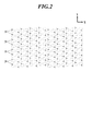
- FIG. 2 is a diagram illustrating an arrangement example of the plurality of nozzles N in the XY plane.
- the inkjet head 1 is provided with, for example, a plurality of nozzle rows in the X direction by a plurality of nozzles N provided along the Y direction.
- the nozzles in the leftmost nozzle row are denoted by reference numerals, and the other nozzles N are omitted.
- FIG. 3 is a cross-sectional view of the inkjet head 1.
- four nozzles N among the plurality of nozzles N are illustrated.
- the plurality of nozzles N are formed on the nozzle substrate 10.
- a plurality of substrates and the like are stacked along the Z direction. Specifically, for example, the pressure chamber substrate 20, the vibration plate 30, the spacer substrate 40, and the wiring substrate 50 are stacked from the side close to the nozzle substrate 10.
- a structure including a plurality of substrates in which the nozzle substrate 10, the pressure chamber substrate 20, the vibration plate 30, the spacer substrate 40, and the wiring substrate 50 are stacked is referred to as a stacked body A.
- a predetermined direction in which ink is ejected is described as “downward” with the nozzle substrate 10 as a reference, and the opposite direction is described as “upward”.
- FIG. 4 is an enlarged view of a configuration related to one nozzle N in the cross-sectional view shown in FIG.
- a pressure chamber 21 communicating with the nozzle N is formed in the pressure chamber substrate 20.
- the diaphragm 30 is provided above the pressure chamber 21 and constitutes one surface (upper surface) of the pressure chamber 21. That is, the vibration plate 30 is provided on the opposite side (upper side) to the pressure chamber 21 in a predetermined direction (lower side) in which ink is ejected.
- An actuator 60 is provided on the upper surface of the diaphragm 30. Here, the actuator 60 is in contact with the diaphragm 30.
- the diaphragm 30, the spacer substrate 40, and the wiring substrate 50 are provided with conduction paths 31, 41, 51 communicating with the pressure chamber 21.
- the ink flow path formed by the conduction paths 31, 41, 51 connects the pressure chamber 21 and the common flow path 70 provided above the wiring board 50.
- the common flow path 70 is provided, for example, in a housing 80 standing above the wiring board 50 and connected to an ink supply mechanism (not shown).
- the ink supplied from the ink supply mechanism to the common flow path 70 is supplied to the pressure chamber 21 through the common flow path 70 and the conduction paths 51, 41, 31.
- the ink supplied to the pressure chamber 21 is ejected from the nozzle N by applying pressure to the ink in the pressure chamber 21 by the vibration of the vibration plate 30 according to the operation of the actuator 60.
- the common flow path 70 functions as a supply unit for the ink supplied to the pressure chamber 21.
- the pressure chamber 21 stores ink ejected from the nozzle N.
- the actuator 60 applies a pressure for ejecting ink from the nozzle N to the pressure chamber 21.
- the laminated body A includes the nozzle substrate 10 on which the nozzles N are formed, the pressure chamber substrate 20 on which the pressure chambers 21 are formed, the diaphragm 30 and the actuator 60 that constitute the upper surface of the pressure chambers 21.
- the structure is a head substrate B.
- the wiring board 50 is provided between the ink supply section (common flow path 70) supplied to the pressure chamber 21 and the head substrate B, and the ink conduction path communicates from the supply section to the pressure chamber 21. (Conduction path 51) is formed.
- the actuator 60 is electrically connected to the wiring 52 provided on the wiring board 50.
- the actuator 60 is, for example, a rectangular piezoelectric element having an upper surface and a lower surface along the XY plane.
- the actuator 60 is provided with a first electrode 61 on its upper surface.
- the actuator 60 is provided with a second electrode 62 on its lower surface.
- the first electrode 61 is electrically connected to the wiring 52 provided on the lower surface side of the wiring substrate 50 via the connection portion 90.
- the connection unit 90 is provided to connect the first electrode 61 and the wiring 52 along the Z direction.
- the connection part 90 has bumps 91 formed on the wiring board 50. Specifically, the bump 91 is formed by wire bonding using gold as a material, for example.
- the bump 91 is formed on the lower surface of the wiring 52, for example.
- the wiring 52 is made of, for example, a conductive metal (for example, aluminum) plate provided so that at least the lower surface is a flat surface.
- a conductive material 92 is applied to the lower end side of the bump 91. Specifically, the conductive material 92 is, for example, a conductive adhesive.
- the conductive adhesive is an adhesive mixed with conductive metal powder (for example, silver powder) and has conductivity.
- the connection unit 90 electrically connects the wiring substrate 50 and the actuator 60 via the bump 91 formed on the wiring substrate 50 and the conductive material 92 applied to the bump 91.
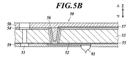
- FIG. 5A to 5C are diagrams showing a process of forming the connection portion 90.
- the wiring board 50 is prepared independently. That is, in the laminate A, the substrates below the spacer substrate 40 are not yet bonded to the wiring substrate 50.
- bumps 91 are formed by wire bonding using gold as shown in FIG. 5B.
- the conductive material 92 is applied to the lower end side of the bump 91 by applying the conductive material 92 using an applicator (not shown).
- 5A to 5C are descriptions relating to the formation of one connection portion 90, but in actuality, the lower surface of each of the plurality of wirings 52 corresponding to each of the plurality of nozzles N included in the inkjet head 1 is used. On the other hand, the formation of the bumps 91 and the application of the conductive material 92 can be performed collectively.
- the wiring board 50 includes, for example, a plate-shaped interposer 53 that is a base of the wiring board 50, insulating layers 54 and 55 that cover the upper surface and the lower surface of the interposer 53, and the insulating layer 54, the interposer 53, and the insulating layer.
- the wiring 52 is connected to a control unit (not shown) related to the application of voltage to the actuator 60 via the through electrode 56 and the wiring 57.
- the second electrode 62 is in contact with the diaphragm 30.
- the diaphragm 30 is a conductor and functions as an electrode that electrically connects the second electrode 62 and the control unit.
- the second electrode 62 is connected to the control unit via, for example, the diaphragm 30 and a wiring (not shown) connected to the diaphragm 30.
- the first electrode 61 is connected to the control unit via the connection unit 90, the wiring 52, the through electrode 56, and the wiring 57, and the second electrode 62 is connected to the diaphragm 30 and a wiring (not shown). By being connected to the control unit, it operates as the actuator 60 under the control of the control unit.
- the spacer substrate 40 secures a space corresponding to the width along the Z direction of the actuator 60 and the connection portion 90 between the diaphragm 30 and the wiring substrate 50.
- the spacer substrate 40 has an opening 42 corresponding to the position where the actuator 60 is disposed on the upper surface side of the diaphragm 30. The opening 42 penetrates the spacer substrate 40 in the Z direction.
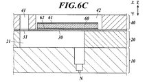
- FIG. 6A to 6C are explanatory views according to a joining example of the diaphragm 30 and the spacer substrate 40.
- FIG. 6A a spacer substrate 40 is prepared. Further, as shown in FIG. 6B, a head substrate B is prepared.
- an actuator 60 is provided on the upper surface of the diaphragm 30. 6C, the spacer substrate 40 and the vibration plate 30 are bonded so that the actuator 60 is positioned at the position of the opening 42 of the spacer substrate 40, and the head substrate B and the spacer substrate 40 are bonded.
- the body is formed.
- the thickness of the spacer substrate 40 corresponds to the width of the actuator 60 and the connecting portion 90 along the Z direction.
- the thickness of the spacer substrate 40 corresponds to the sum of the width of the actuator 60 in the Z direction and the width of the connection portion 90 in the Z direction. More specifically, the thickness of the spacer substrate 40 is, for example, 50 [ ⁇ m] or more and 200 [ ⁇ m] or less.
- the thickness of the spacer substrate 40 affects the length of the conduction path 41 between the common flow path 70 and the pressure chamber 21.
- the shorter the conduction path 41 the smaller the flow path resistance for the ink passing through the conduction path 41. Therefore, since the thickness of the spacer substrate 40 can be further reduced by further reducing the width of the actuator 60 and the connecting portion 90 along the Z direction, the flow path resistance with respect to the ink can be further reduced.
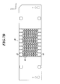
- the spacer substrate 40 has a structure (glue guard) for preventing the adhesive bonding the spacer substrate 40 and the wiring substrate 50 from entering the opening 42 side, and a structure for releasing air (air escape). ) Is provided. Specifically, for example, as shown in FIGS. 7A and 7B, the spacer substrate 40 extends along the Y direction at both ends of a row of the opening portions 42 formed by the opening portions 42 provided along the Y direction. A linear pattern 43 is formed. The pattern 43 functions as a glue guard and an air escape. More specifically, the spacer substrate 40 is subjected to photolithography on both sides in order to form the opening 42. Here, by forming the pattern 43 only on one surface (upper surface), a linear counterbore is formed on the surface.
- the openings 42 adjacent to each other along the Y direction are continuous.
- the pattern 43 is formed so that it may continue from the opening part 42 located in the both ends of the row
- FIG. Accordingly, when the bonded body of the head substrate B and the spacer substrate 40 shown in FIG. 6C and the wiring substrate 50 on which the connection portion 90 shown in FIG. 5A is bonded by heating, the volume is increased by heating. Increasing air in the opening 42 can escape from the pattern 43. That is, the pattern 43 functions as an air escape.
- the adhesive for bonding between the spacer substrate 40 and the wiring substrate 50 comes into contact with the frame portion on the upper plate surface of the spacer substrate 40 shown in FIG. 7B. If there is, surplus adhesive will move along the upper plate surface in search of a destination.
- the pattern 43 since the pattern 43 exists, excess adhesive does not enter the pattern 43 and enter the opening 42. That is, the pattern 43 functions as a glue guard.
- FIG. 7 among the many existing openings 42, patterns 43, and actuators 60, reference numerals are given to the leftmost four, and the remaining reference numerals of the same configuration are omitted.
- the pressure chamber substrate 20, the diaphragm 30, the wiring substrate 50, and the spacer substrate 40 each have a difference in thermal expansion coefficient that is a predetermined value or less.
- “the difference between the respective thermal expansion coefficients is equal to or less than a predetermined value” means that the difference between the respective thermal expansion coefficients of the pressure chamber substrate 20, the vibration plate 30, the wiring substrate 50, and the spacer substrate 40 is the respective substrate. This is a range that does not cause problems due to warping.
- the material of the pressure chamber substrate 20, the vibration plate 30, and the wiring substrate 50 is silicon (Si).
- the material of the spacer substrate 40 is 42 alloy. More specifically, the pressure chamber substrate 20 and the diaphragm 30 are entirely made of silicon.
- the interposer 53 is formed of silicon. Since the interposer 53 is configured to occupy most of the configuration of the wiring substrate 50, the interposer 53 is formed of silicon, so that the thermal expansion coefficient of the wiring substrate 50 can be changed to the pressure chamber substrate 20 and the diaphragm. 30 can be substantially the same.
- 42 alloy which is a material of the spacer substrate 40 is an alloy composed of nickel [42]%, iron [57]% by weight, and the balance of a small amount of additive substances (for example, copper, manganese, etc.). .
- the thermal expansion coefficient of silicon is 2.5 ⁇ 10 ⁇ ⁇ 6 [1 / ° C.] to 4.0 ⁇ 10 ⁇ ⁇ 6 [1 / ° C.].
- the thermal expansion coefficient of 42 alloy is 4.5 ⁇ 10 ⁇ ⁇ 6 [1 / ° C.] to 6.0 ⁇ 10 ⁇ ⁇ 6 [1 / ° C.].
- both the thermal expansion coefficient of silicon and the thermal expansion coefficient of 42 alloy are extremely small.
- the difference between the thermal expansion coefficient of silicon and that of 42 alloy is 0.5 ⁇ 10 ⁇ ⁇ 6 [1 / ° C.] to 3.5 ⁇ 10 ⁇ ⁇ 6 [1 / ° C.].
- the predetermined value is 3.5 ⁇ 10 ⁇ -6 [ 1 / ° C.].
- the thermal expansion coefficient of silicon and the thermal expansion coefficient of 42 alloy are substantially the same.
- each material of the pressure chamber substrate 20, the vibration plate 30, the wiring substrate 50, and the spacer substrate 40 is ink-jetted by peeling between the substrates due to the warpage of the substrates that may be caused by the difference in thermal expansion coefficient between them.
- the electrical connection (for example, the connection part 90 etc.) in the head 1 is determined within a range in which the connection is not broken.
- the spacer substrate 40 has the maximum thickness (200 [ ⁇ m]) assumed in this embodiment, the inkjet head 1 is changed from normal temperature (for example, around 25 [° C.]) to 80 [° C.]. If the degree of peeling between the substrates is 0.16 [ ⁇ m] or less, there is no problem.
- the condition required for the substrate material to realize such a degree of peeling is a thermal expansion coefficient of 10 ⁇ 10 ⁇ ⁇ 6 [1 / ° C.] or less.
- the above is an example in the case where the spacer substrate 40 has the maximum thickness (200 [ ⁇ m]) assumed in the present embodiment.
- the spacer substrate 40 Since the degree of thermal expansion is reduced, the upper limit of the thermal expansion coefficient is more relaxed.
- the thermal expansion coefficient required for the material can be appropriately changed according to the specific configuration, but it is considered that it should be 10 ⁇ 10 ⁇ ⁇ 6 [1 / ° C.] or less.
- Both silicon and 42 alloy are materials showing a thermal expansion coefficient lower than 10 ⁇ 10 ⁇ ⁇ 6 [1 / ° C.].
- the material of the nozzle substrate 10 is silicon. Since the nozzle substrate 10 is made of silicon, the thermal expansion coefficient of the nozzle substrate 10 is substantially the same as the thermal expansion coefficients of the pressure chamber substrate 20, the vibration plate 30, the wiring substrate 50 and the spacer substrate 40. Therefore, the difference between the thermal expansion coefficient of the nozzle substrate 10 and the thermal expansion coefficient of the other substrate, such as preventing leakage of ink from the gap due to the peeling between the nozzle substrate 10 and the pressure chamber substrate 20. It is possible to prevent the occurrence of problems due to warpage that may occur due to the
- the nozzle N is formed by dry etching on the nozzle substrate 10, for example.
- the accuracy of the position and diameter of the nozzle N can be made higher. That is, since the amount of ink ejected from the nozzle N and the ejection position can be adjusted with higher accuracy, it is possible to provide the inkjet head 1 that can eject ink with higher accuracy. it can.
- the pressure chamber substrate 20, the diaphragm 30, the wiring substrate 50, and the spacer substrate 40 are made of a material having a thermal conductivity of 10 [W ⁇ m ⁇ 1 ⁇ K ⁇ 1 ] or more.
- the thermal conductivity of silicon, which is a material of the pressure chamber substrate 20, the vibration plate 30, and the wiring substrate 50 is 168 [W ⁇ m ⁇ 1 ⁇ K ⁇ 1 ].
- the thermal conductivity of 42 alloy which is a material of the spacer substrate 40 is 15 [W ⁇ m ⁇ 1 ⁇ K ⁇ 1 ].
- the material of the pressure chamber substrate 20, the vibration plate 30, the wiring substrate 50, and the spacer substrate 40 has a thermal conductivity of 10 [W ⁇ m ⁇ 1 ⁇ K ⁇ 1 ] or more, so that the laminate can be obtained. Since the temperature can be made uniform in the temperature distribution in A, particularly the temperature distribution in the surface direction, the temperature of the plurality of nozzles N can be made uniform, and the temperature condition of each nozzle N can be made substantially the same.
- the plurality of nozzles N of the inkjet head 1 have different heat amounts due to the difference in the injection rate of each nozzle N, but the laminated body A has a thermal conductivity of 10 [W ⁇ m ⁇ 1 ⁇ K ⁇ 1 ].
- the spacer substrate 40 is subjected to a surface treatment.
- the spacer substrate 40 is subjected to, for example, nickel (Ni) plating as a surface treatment.
- the surface treatment is performed after the spacer substrate 40 is subjected to shape processing such as the conduction path 41 and the opening 42. Since the spacer substrate 40 can obtain resistance to rust and solvent by surface treatment, the durability of the spacer substrate 40 can be further improved.
- the conductive path 41 is provided in the spacer substrate 40, the surface treatment functions effectively in order to ensure resistance to the solvent and the like contained in the ink.
- the surface treatment is not limited to the plating treatment with nickel (Ni), but may be any surface treatment that can obtain rust prevention and resistance to solvents.
- a treatment for forming a film made of ethyl silicate such as TEOS (Tetraethyl orthosilicate) or a film made of a paraxylylene polymer such as Parylene (registered trademark) on the surface of the spacer substrate 40 may be used.
- a specific process for forming the film for example, a vapor deposition process such as sputtering can be used.
- the pressure chamber substrate 20, the vibration plate 30, the wiring substrate 50, and the spacer substrate 40 have a difference in thermal expansion coefficient that is not more than a predetermined value. Prevent occurrence of problems due to substrate warpage or separation between substrates due to differences in thermal expansion coefficients between substrates, such as changes in the ink ejection angle from nozzles N and leakage of ink from separation portions between substrates. Can do.
- each component constituting the inkjet head 1 is made. Since the temperature can be made uniform in the temperature distribution of the substrate, particularly the temperature distribution in the surface direction, the temperature of the plurality of nozzles N becomes uniform, and the temperature condition of each nozzle N can be made substantially the same. As a result, the variation in the ejection characteristics of the ink that can be caused by the temperature difference between the nozzles N can be further reduced, so that the ink can be ejected with higher accuracy.
- the material of the pressure chamber substrate 20, the diaphragm 30, and the wiring substrate 50 is silicon
- the material of the spacer substrate 40 is an alloy in which 42% nickel is mixed with iron, it is generally available. With a possible material, it is possible to manufacture the inkjet head 1 with higher reliability that can prevent the occurrence of problems due to the warpage of the substrates due to the difference in thermal expansion coefficient between the substrates and the separation between the substrates.
- the thickness of the spacer substrate 40 is 50 [ ⁇ m] or more and 200 [ ⁇ m] or less, the thinness of the spacer substrate 40 can suppress the degree of thermal expansion of the spacer substrate 40 to a minimum. It is possible to more reliably prevent the occurrence of problems due to the warpage of the substrate due to the difference in thermal expansion coefficient between the two and the separation between the substrates.
- the conduction path 41 when the conduction path 41 is formed in the spacer substrate 40 as in the present embodiment, the conduction path 41 can be shortened due to the thinness of the spacer substrate 40, so that the flow path resistance against ink is further increased. Can be small.
- the spacer substrate 40 is subjected to a surface treatment, rust resistance and resistance to solvents can be obtained, so that the durability of the spacer substrate 40 can be further improved.
- the material of the nozzle substrate 10 is silicon, it is possible to prevent the occurrence of problems due to warpage that may occur due to the difference between the thermal expansion coefficient of the nozzle substrate 10 and the thermal expansion coefficient of other substrates.
- the nozzle N is formed by dry etching with respect to the nozzle substrate 10, the accuracy of the position and the diameter of the nozzle N can be made higher, so the amount of ink discharged from the nozzle N The ejection position can be adjusted with higher accuracy, and the inkjet head 1 that can eject ink with higher accuracy can be provided.
- the actuator 60 is not damaged by heat and vibration associated with the formation of the bumps 91, and the yield of the inkjet head 1 is further improved in the manufacture of the inkjet head 1. be able to.
- the actuator 60 is a piezoelectric element as in the present embodiment
- the bump 91 is formed on the piezoelectric element side, the bump 91 and the first electrode
- the bump 91 is formed on the lower surface side of the wiring 52 provided so that the lower surface is a flat surface. Good adhesion between the bump 91 and the wiring 52 can be ensured.
- the conductive material 92 is applied to the bump 91, the bump 91 and the actuator 60 can be connected by the conductive material 92 by the conductive material 92. Therefore, the actuator 60 is connected by the bump 91 and the conductive material 92.
- the wiring board 50 can be connected better.
- the conductive material 92 is a conductive adhesive, in addition to being able to easily apply the conductive material 92 to the bumps 91, the conductive material 92 is bonded to the actuator 60. Since it can be performed easily, the process relating to the manufacture of the inkjet head 1 including the connection between the actuator 60 and the wiring substrate 50 can be made easier.
- a conductive adhesive is used as the conductive material 92, but this is an example and the present invention is not limited to this.
- the conductive material 92 may be solder.
- the solder can be used as the conductive material 92 by applying cream solder to the wiring board 50 on which the bumps 91 are formed as shown in FIG.
- the conductive material 92 can be collectively applied to the plurality of bumps 91 corresponding to the plurality of nozzles N.
- a paste containing 60% to 70% of silver can also be used as the conductive material 92.
- Silicon is used for the diaphragm 30 and the wiring substrate 50
- 42 alloy is used for the spacer substrate 40, but this is an example and the present invention is not limited to this. That is, the description does not use any other material in which the difference in thermal expansion coefficient among the pressure chamber substrate 20, the diaphragm 30, the spacer substrate 40, and the wiring substrate 50 is equal to or less than a predetermined value at present and in the future. It is not a hindrance.
- the entire spacer substrate 40 is subjected to the surface treatment, but this is an example and the present invention is not limited to this. As long as the surface treatment is applied to the conduction path 41 provided in the spacer substrate 40, the antirust property and the resistance to the solvent related to the contact with the ink can be ensured.
- the structure of the laminated body A in said embodiment is an example to the last, Comprising: It is not restricted to this.
- another substrate intermediate substrate 100
- the intermediate substrate 100 is provided, for example, for the purpose of providing the conduction path 101 between the nozzle substrate 10 and the pressure chamber substrate 20.
- the shape of the flow path of the ink reaching the nozzle N can be more easily set to an arbitrary shape, such as a shape in which the diameter of the path through which the ink passes is reduced.
- the shape of the ink path for adjusting the kinetic energy applied to the ink in relation to the ejection of the ink can be adjusted more easily.
- the difference in thermal expansion coefficient between the intermediate substrate 100 and other substrates is not more than a predetermined value.
- the intermediate substrate 100 is made of, for example, silicon, so that the difference in thermal expansion coefficient from other substrates can be set to a predetermined value or less.
- the pressure chamber substrate 20 and the diaphragm 30 are separately provided and stacked, but this is an example and the present invention is not limited thereto.
- the pressure chamber substrate 20 and the diaphragm 30 may be integrally formed.
- the present invention can be used for an inkjet head.
Landscapes
- Particle Formation And Scattering Control In Inkjet Printers (AREA)
Abstract
Priority Applications (3)
| Application Number | Priority Date | Filing Date | Title |
|---|---|---|---|
| US14/891,571 US9539811B2 (en) | 2013-05-15 | 2014-05-12 | Inkjet head |
| EP14797930.6A EP2998120B1 (fr) | 2013-05-15 | 2014-05-12 | Tête à jet d'encre |
| JP2015517069A JPWO2014185370A1 (ja) | 2013-05-15 | 2014-05-12 | インクジェットヘッド |
Applications Claiming Priority (2)
| Application Number | Priority Date | Filing Date | Title |
|---|---|---|---|
| JP2013103205 | 2013-05-15 | ||
| JP2013-103205 | 2013-05-15 |
Publications (1)
| Publication Number | Publication Date |
|---|---|
| WO2014185370A1 true WO2014185370A1 (fr) | 2014-11-20 |
Family
ID=51898348
Family Applications (1)
| Application Number | Title | Priority Date | Filing Date |
|---|---|---|---|
| PCT/JP2014/062561 Ceased WO2014185370A1 (fr) | 2013-05-15 | 2014-05-12 | Tête à jet d'encre |
Country Status (4)
| Country | Link |
|---|---|
| US (1) | US9539811B2 (fr) |
| EP (1) | EP2998120B1 (fr) |
| JP (1) | JPWO2014185370A1 (fr) |
| WO (1) | WO2014185370A1 (fr) |
Cited By (1)
| Publication number | Priority date | Publication date | Assignee | Title |
|---|---|---|---|---|
| JPWO2017047533A1 (ja) * | 2015-09-18 | 2018-07-05 | コニカミノルタ株式会社 | インクジェットヘッド及びインクジェット記録装置 |
Citations (7)
| Publication number | Priority date | Publication date | Assignee | Title |
|---|---|---|---|---|
| JP2002248775A (ja) * | 2000-12-19 | 2002-09-03 | Kyocera Corp | インクジェットヘッド及びそれを用いたインクジェットプリンタ |
| JP2006168249A (ja) * | 2004-12-17 | 2006-06-29 | Ricoh Printing Systems Ltd | インクジェットヘッド及びインクジェットヘッドの制御方法並びにインクジェットヘッドの洗浄方法 |
| JP2006334975A (ja) * | 2005-06-03 | 2006-12-14 | Fujifilm Holdings Corp | 液体吐出ヘッド |
| JP2007083484A (ja) * | 2005-09-21 | 2007-04-05 | Fuji Xerox Co Ltd | 液滴吐出ヘッド、及び、液滴吐出ヘッド製造方法 |
| JP2010069750A (ja) * | 2008-09-19 | 2010-04-02 | Seiko Epson Corp | インクジェット式記録ヘッド及びその製造方法、インクジェット式記録装置 |
| JP2012061689A (ja) * | 2010-09-15 | 2012-03-29 | Ricoh Co Ltd | 液滴吐出ヘッド、液滴吐出ヘッドの製造方法、液体カートリッジ及び画像形成装置 |
| JP4929755B2 (ja) | 2005-02-23 | 2012-05-09 | 富士ゼロックス株式会社 | 液滴吐出ヘッド及び液滴吐出装置 |
Family Cites Families (6)
| Publication number | Priority date | Publication date | Assignee | Title |
|---|---|---|---|---|
| WO2003061975A1 (fr) * | 2002-01-16 | 2003-07-31 | Xaar Technology Limited | Appareil de depot de gouttelettes |
| JP4306717B2 (ja) * | 2006-11-09 | 2009-08-05 | セイコーエプソン株式会社 | シリコンデバイスの製造方法及び液体噴射ヘッドの製造方法 |
| JP2011115972A (ja) * | 2009-12-01 | 2011-06-16 | Konica Minolta Holdings Inc | インクジェットヘッド |
| US8297742B2 (en) * | 2010-03-19 | 2012-10-30 | Fujifilm Corporation | Bonded circuits and seals in a printing device |
| JP2011218641A (ja) * | 2010-04-08 | 2011-11-04 | Konica Minolta Holdings Inc | インクジェットヘッド |
| JP5975030B2 (ja) * | 2011-06-22 | 2016-08-23 | コニカミノルタ株式会社 | インクジェットヘッドの製造方法、及び、インクジェット描画装置の製造方法 |
-
2014
- 2014-05-12 WO PCT/JP2014/062561 patent/WO2014185370A1/fr not_active Ceased
- 2014-05-12 EP EP14797930.6A patent/EP2998120B1/fr active Active
- 2014-05-12 US US14/891,571 patent/US9539811B2/en active Active
- 2014-05-12 JP JP2015517069A patent/JPWO2014185370A1/ja active Pending
Patent Citations (7)
| Publication number | Priority date | Publication date | Assignee | Title |
|---|---|---|---|---|
| JP2002248775A (ja) * | 2000-12-19 | 2002-09-03 | Kyocera Corp | インクジェットヘッド及びそれを用いたインクジェットプリンタ |
| JP2006168249A (ja) * | 2004-12-17 | 2006-06-29 | Ricoh Printing Systems Ltd | インクジェットヘッド及びインクジェットヘッドの制御方法並びにインクジェットヘッドの洗浄方法 |
| JP4929755B2 (ja) | 2005-02-23 | 2012-05-09 | 富士ゼロックス株式会社 | 液滴吐出ヘッド及び液滴吐出装置 |
| JP2006334975A (ja) * | 2005-06-03 | 2006-12-14 | Fujifilm Holdings Corp | 液体吐出ヘッド |
| JP2007083484A (ja) * | 2005-09-21 | 2007-04-05 | Fuji Xerox Co Ltd | 液滴吐出ヘッド、及び、液滴吐出ヘッド製造方法 |
| JP2010069750A (ja) * | 2008-09-19 | 2010-04-02 | Seiko Epson Corp | インクジェット式記録ヘッド及びその製造方法、インクジェット式記録装置 |
| JP2012061689A (ja) * | 2010-09-15 | 2012-03-29 | Ricoh Co Ltd | 液滴吐出ヘッド、液滴吐出ヘッドの製造方法、液体カートリッジ及び画像形成装置 |
Cited By (1)
| Publication number | Priority date | Publication date | Assignee | Title |
|---|---|---|---|---|
| JPWO2017047533A1 (ja) * | 2015-09-18 | 2018-07-05 | コニカミノルタ株式会社 | インクジェットヘッド及びインクジェット記録装置 |
Also Published As
| Publication number | Publication date |
|---|---|
| US9539811B2 (en) | 2017-01-10 |
| JPWO2014185370A1 (ja) | 2017-02-23 |
| EP2998120A4 (fr) | 2017-08-09 |
| EP2998120A1 (fr) | 2016-03-23 |
| US20160144625A1 (en) | 2016-05-26 |
| EP2998120B1 (fr) | 2019-05-08 |
Similar Documents
| Publication | Publication Date | Title |
|---|---|---|
| JP6295684B2 (ja) | インクジェットヘッド及びインクジェット記録装置 | |
| US8585187B2 (en) | High density electrical interconnect for printing devices using flex circuits and dielectric underfill | |
| KR100915281B1 (ko) | 액체 토출 헤드 및 그 제조 방법 | |
| US7964955B2 (en) | Electronic device package and electronic equipment | |
| JP5405339B2 (ja) | 配線回路基板及びその製造方法 | |
| JP5309686B2 (ja) | インクジェットヘッド | |
| WO2014185369A1 (fr) | Tête à jet d'encre et son procédé de fabrication | |
| JP5034593B2 (ja) | 駆動回路付き配線基板の構造および液滴吐出ヘッド | |
| WO2012176874A1 (fr) | Tête à jet d'encre et dispositif d'impression à jet d'encre | |
| JP6044258B2 (ja) | インクジェットヘッド | |
| WO2014185370A1 (fr) | Tête à jet d'encre | |
| US7571993B2 (en) | Ink-jet head | |
| JP2011240549A (ja) | 液体噴射ヘッド及び液体噴射ヘッドの製造方法 | |
| JP6330819B2 (ja) | 配線基板及びインクジェットヘッド | |
| JP5821183B2 (ja) | インクジェットヘッドユニット及びインクジェットヘッドユニットの製造方法 | |
| JP2010232383A (ja) | 電子装置及びその製造方法 | |
| JP2015150793A (ja) | 配線実装構造の製造方法、液体噴射ヘッドの製造方法及び配線実装構造 | |
| US9517624B2 (en) | Wiring mounting structure and method of manufacturing the same, and liquid ejecting head and liquid ejecting apparatus | |
| JP2015229314A (ja) | インクジェットヘッド及びインクジェットヘッドの製造方法 | |
| JP4867252B2 (ja) | 積層体の製造方法及びインクジェットヘッドの製造方法 | |
| JP2018192674A (ja) | 液体吐出ヘッドおよびその製造方法 | |
| JP6879138B2 (ja) | インクジェットヘッド及びインクジェット記録装置 | |
| JP2022165220A (ja) | 液体吐出ヘッドの製造方法 | |
| JP2016060177A (ja) | 液体噴射ヘッド及びその製造方法並びに液体噴射装置 | |
| JP2010232375A (ja) | 電子装置及び電子装置の製造方法 |
Legal Events
| Date | Code | Title | Description |
|---|---|---|---|
| 121 | Ep: the epo has been informed by wipo that ep was designated in this application |
Ref document number: 14797930 Country of ref document: EP Kind code of ref document: A1 |
|
| ENP | Entry into the national phase |
Ref document number: 2015517069 Country of ref document: JP Kind code of ref document: A |
|
| NENP | Non-entry into the national phase |
Ref country code: DE |
|
| WWE | Wipo information: entry into national phase |
Ref document number: 14891571 Country of ref document: US Ref document number: 2014797930 Country of ref document: EP |